Schottky Barrier Diode Video Detectors Application Note 923
Schottky Barrier Diode Video Detectors Application Note 923
Schottky Barrier Diode Video Detectors Application Note 923

You also want an ePaper? Increase the reach of your titles
YUMPU automatically turns print PDFs into web optimized ePapers that Google loves.
5<strong>Diode</strong> and System Parameters<strong>Diode</strong> HP 5082-2750: f N = 3 kHz, I d = 20 µA, f = 10 GHz,R A = 0.5 kΩ, B v = 2 MHz, R s = 25 ΩWe get the following:5 log28R A +I dR S C 2 j(i) f 210 log 1 += 3.0 dBI d1 +f NB VB V1nfL10 log I d5 log B VTotal Degradation≅ 1.4 dB= 13.0 dB= 31.5 dB= 48.9 dB50,,,æææ,,,æææNOISE TEMPERATURE RATIO (dB)403020TYPICAL POINT CONTACT DIODES(BIASED FOR OPTIMUM TSS)TYPICALHP 5082-27502755, 282410DC BIAS =TYPICAL20 µAf N = 1 MHzf N =0 3 kHz-5102 10 3 104 105 106 107FREQUENCY (Hz)Figure 4. Flicker NoiseCharacteristics of HP Detector <strong>Diode</strong>sExpected TSS = -107 + 48.8 = -58.1 dBmThis is typical of the HP 5082-2750 diode which is specified at -55 dBmto allow for reasonable variations in diode parameters. Thesignificance of the above is the relative magnitude of the variousdegradation factors in a particular system. The degradation due todiode flicker and shot noise is particularly low due to the low flickernoise corner frequency for this diode when it is operated at theoptimum bias of 20 µA. The typical flicker noise characteristics of theHP 5082-2750 and 5082-2824 diodes are shown in Figures 4 and 5.Figure 4 shows the flicker noise characteristic as a function of videofrequency at 20 µA bias, and Figure 5 shows the change in the noisecorner frequency f N as a function of bias. Even at high bias levels, f N issufficiently low, i.e., 30 kHz, by comparison to normal videobandwidths, typically > 300 kHz, that the flicker noise contribution canbe considered negligible. This can be seen in Figure 6 in which thefactor5 log28R A +I d1 +f NB VB V1nfLfN – NOISE CORNER FREQUENCY (KHz)1001011 10 100BIAS CURRENT (µA)Figure 5. Noise Corner Frequency vs.Bias (Typical HP 5082-2750, 5082-2755)100010.0of Eq. (5) is plotted as a function of B v with f L fixed at 100 Hz. Formost applications of the HP Detector <strong>Diode</strong>s, this factor can besimplified to:5 logR A +28I d(7)∆TSS – TANGENTIAL SENSITIVITY (dB)8.06.04.02.0F N = 1.0 MHzF N = 0.1 MHzF N = 0.01 MHzF N = 0.003 MHzF L = 0.1 KHz00.1 0.2 0.4 1.0 2.0 4.0 8.0 10.0VIDEO BANDWIDTH (MHz)Figure 6. Amplifier and <strong>Diode</strong> NoiseContribution as a Function of <strong>Video</strong>Bandwidth
6IV. Bandwidth RequirementsTo maintain high sensitivity, the video bandwidth of the video detectorshould be no greater than necessary to recover the modulationinformation. The bandwidth required for pulse recovery depends onthe nature of the information to be gained from the pulse. For example,in pulse search radar, peak pulse detectability is more significant thanpulse shape. In ferret systems, instrumentation, or data transmissionsystems, the resolution of the fine details of the pulse shape, i.e.,risetime and pulsewidth, may be of much greater importance in spite ofgreater bandwidth requirements.For maximum pulse detectability, the video bandwidth should be madejust sufficient enough to maximize the output signal-to-noise ratio ofthe detecting system. This condition occurs when the video circuittransfer function is matched to the spectrum of the signalwaveform [4,5]; i.e., for a rectangular pulse and a rectangular low passfilter response, the required filter bandwidth isB V ≅ 1/t w (8)wheret w = PulsewidthFor a simple RC filter, which is the usual case at the output of thedetector diode, the maximum S/N occurs when the filter’s upper 3 dBvideo frequency is approximately:f u(3 dB) ≅0.25(9)t wIn other applications, it may be desirable to resolve the shape of thepulse, i.e., risetime, pulsewidth and flat amplitude. To resolve therisetime of the pulse, the upper 3 dB frequency of the video circuit willhave to bef u(3 dB) ≅ 0.35/t r (10)where t r = Pulse risetimeTo resolve the shape of the pulse to any degree of accuracy,consideration must also be given to how much amplitude droop ispermissible. Amplitude droop depends on the low frequency 3 dB pointand is given by:Droop %f L(3 dB) = (11)600 t w
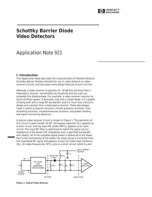
7V. Design Considerations for <strong>Video</strong> DetectorThe basic video detector circuit and its equivalent representations atboth the RF and video ports are shown in Figure 7.C PDIODEDC BIASL PR SRFPORTC JR LVIDEOPORT(a) COMPLETE VIDEO DETECTOR CIRCUITL PR SR JR JR VRFSIGNALC b C AC P C bCC AJR Le VC b R V + R S + R J(b) EQUIVALENT CIRCUIT ATTHE RF PORT(c) EQUIVALENT CIRCUIT AT THEVIDEO PORTFigure 7. <strong>Video</strong> Detector Equivalent Circuits(A) <strong>Video</strong> Circuit Design ConsiderationsIn the video circuit, R L represents the load or amplifier inputresistance, and C A represents the amplifier input capacitance as well asall the stray and particularly cable capacitances that may be present inthe video circuit. These R and C elements will impose a limit on theupper 3 dB cut-off frequency of this circuit, which is given by:f u(3 dB) =1(12)2 π R T C TR V R LwhereR T =R V + R L(13)andC T = C b + C A(14)In most video detector designs, this circuit has a greater influence onthe effective video bandwidth than the bandwidth of the amplifier. TheR T C T time constant can be reduced by reducing all the element valueswithin certain limits. A severe reduction in the value of the RF bypasscapacitance C b will lead to poor RF/video isolation and a decrease inthe signal level delivered to the diode. The reactance of this capacitorat the operating frequency should be kept to less than 10% of the RFimpedance of the diode. At low RF frequencies and wide video
8bandwidths, this capacitor can be replaced by a low pass filterstructure as shown in Figure 8 with a cut-off frequency f c ≤ 1 / 2 f rf .Because this filter is required to pass fast pulses, the design should befor flat time delay rather than for equal-ripple.A reduction in stray and amplifier capacitances is always advisable andin wideband designs is often necessary. One suitable technique whichis particularly effective when cable interconnections must be madebetween the detector circuit and the video amplifier is shown in Figure9. In this circuit, the original cable capacitance C o is reduced byfeedback to: C eff = C o (1 - A v ) where A v is the total gain from the inputof the amplifier to the first shield and must be < 1.R VFigure 8. Low Pass <strong>Video</strong> CouplingStructureTRIAXIAL CABLETODETECTORTO FEEDBACKLOOPFigure 9. Circuit for Reducing Cable CapacitanceAlternately, either R L or R v can be reduced. The amount that R L can bereduced is often limited if voltage amplification is desired since theoutput voltage of the detector is maximized by making R L large. R v ofthe diode can be lowered by increasing the bias current. Although thisresults in reduced sensitivity, as was shown in Figure 2, it maynevertheless be needed to achieve the required video bandwidth. Areduction of video resistance has other beneficial effects. It can, forinstance, be adjusted to be the optimum source resistance value for aminimum noise figure of the video amplifier. When this is desired, R vshould be adjusted so thatR V ≅ R NS R NP(15)whereR NS = Equivalent series noise resistance of amplifierR NP = Equivalent parallel noise resistance of amplifierThis is usually in the range of 400 - 2000 ohms for most low noisetransistor input stages.
9(B) RF Circuit Design ConsiderationsThe RF circuit consists essentially of a filter structure that is designedto match the signal source resistance, usually 50 ohms, to the diodejunction resistance, R j . The equivalent circuit of the diode at RF isshown in Figure 7b. The presence of R S and C j introduces a loss ofsignal which is dependent on frequency and the magnitudes of R S , C j ,and R j . This dependence is given byL + ω 2 C 2 db = 10 log 1 + R Sj R S R j (16)R jwhereω = 2πfSince R j is a function of bias current, i.e., R j ≅ 28/I d , the above can berestated as28ω 2 C 2 j RL Sdb = 10 log 1 + R SI d+28 I d(17)from which it is obvious that the RF loss can be minimized at any givenfrequency by biasing the diode. This effect was included as one of thebias dependent parameters in the TSS expression (Eq. 5), which wasthen used to determine optimum bias with respect to maximum TSS ata given frequency. Bias also affects the RF impedance of the diode, andthe impedance that is obtained at a bias corresponding to maximumTSS is not necessarily optimum for achieving broadband RF matchingto the diode.The typical measured RF impedances for HP 5082-2750 and 5082-2755diodes, which are the same chip in two different packages, are shownas a function of frequency in Figure 10. Figure 10 shows the diodewhen it is biased at 20 µA (R j ≅ 1400), which is its optimum bias formaximum sensitivity at 10 GHz. As can be seen, the SWR for eitherpackage style is high over most of the frequency range and normallyeither diode will have to be matched to the source with additionalreactive elements. Practical reactances, however well made, willintroduce additional losses in the matching structure. Furthermore, thefarther these reactances are placed from the diode chip, the more losswill be introduced due to high standing waves and current maximapoints due to high standing waves and current maxima points betweenthem. Even well made double-stub tuners can introduce losses as highas 1.5 - 2 dB. The impedance plots of Figure 10 also clearly illustratethe effect that package and chip parasitics can have on the RFimpedance of the diode. Assuming that the RF bypass capacitor C b isproperly chosen and can be neglected, which was the case for theimpedance plots, the RF admittance of the remaining circuit can beexpressed as1Y 12 = jωC P +1(18)R S + jωL P +1jωC j +R j0.2-.2.4.6.81.01.58 GHz.2 .4 .6 .8 1.0 1.5 3 4 5 10TYPICALHP 5082-27502 GHz 2 GHz12 GHz4 GHz10 GHz6 GHz8 GHz4 GHz6 GHz-.4-.6TYPICALHP 5082-2755-.810 GHz-1.0-1.5212 GHz-23-34510-10-5-4Figure 10. Typical RF Impedance ofHP 5082-2750 and 5082-2755 <strong>Diode</strong>sat Bias Current of 20 µA0
10This admittance has two potential resonant frequencies. Neglecting R Sand R j , these resonant frequencies can be expressed approximately as:ω P ≅ω S ≅1L P C j1 1+L P C j L P C P(19)(20)As can be seen from the plots, a resonant frequency for the highinductance glass package is evident at ≅ 7.9 GHz.Due to the low values of the parasitic elements, the pill packageddevice 5082-2750 does not exhibit any resonances up to a frequency of12 GHz. Such a diode can be brought into match over fairly broadbandwidths by a series length of line and a quarterwave transformer [6].To simplify broadband matching, the impedance of the diode can bereduced by using more DC bias than would normally be required formaximum TSS. Figure 11 illustrates the magnitude of the effect thatbias has on the RF impedance. These plots are made for the samediodes as in Figure 9, but at a bias of 330 µA. The 5082-2750 pillpackaged diode impedance is now within a SWR of : 2/1 over most ofits useful frequency range. Although there will also be a reduction ofsensitivity of about 7 dB, as was shown in Figure 2, nevertheless, thetrade-off may be worthwhile in broadband systems.VI. Dynamic RangeIn addition to achieving high sensitivity, video detectors are usuallyrequired to have a large dynamic range. Usually this statement refers tothe “square-law” range as shown in Figure 12 and is the range overwhich the output signal voltage is proportional to the input signalpower, i.e.:V s = γP in (21)where γ is the diode voltage sensitivity at the specified frequency andbias. Deviation from square-law characteristic occurs when γ departsfrom a constant value. This will occur when the RF carrier and,consequently, the rectified current become high enough to appreciablyaffect the quiescent bias current, I d . At HP, the upper limit of squarelawoperation is defined to be the power level which is 0.5 dB higherthan the power level that would produce the same output voltage if γhad remained constant.As can be seen from Figure 12, the transfer characteristic of a <strong>Schottky</strong><strong>Barrier</strong> <strong>Diode</strong> does not simply saturate beyond this point but merelychanges from square-law to linear, which then continues to a higherpower level before saturation. This range is defined as the lineardynamic range and can be appreciable if the breakdown voltage of thediode is high. For example, the HP 5082-2824 detector diode is rated at0.2-.2.4.6.81.01.5TYPICALHP 5082-2750 14 GHz6 GHz.2 .4 .6 .8 1.0 1.5 3 4 5 102 GHz10 GHz2 GHz 16 GHz-.4-.6-.816 GHz6 GHz-1.0-1.52TYPICALHP 5082-275510 GHzFigure 11. Typical RF Impedance ofHP 5082-2750 and 5082-2755 <strong>Diode</strong>sat Bias Current of 330 µAEOUT – VOLTAGE OUT10V1V100 mV10 mV1 mV100 µV10 µV-23-34510-10-5-4FREQUENCY - 2 GHz (HP 5082-2824)FREQUENCY - 10 GHz (HP 5082-2750,-2755)I BIAS = 20 µAR L = 5 KΩSQUARE LAWLINEAR2824HP 2750-2755-60 -40 -20 0 20 40P IN – POWER INPUT (dBm)Figure 12. Detector DynamicCharacteristics0
11a breakdown voltage of 15 V. By contrast, point contact diodes whosebreakdown voltage is generally low (2 - 3 V), do not exhibit a broadlinear range. For applications that require monitoring of high level RFsignals, i.e., radio controlled trigger circuits, high power monitors, orRF proximity fuses, this range is very useful. <strong>Application</strong>s that are notcritical of the change in the transfer characteristics can utilize the verylarge total (square-law and linear) dynamic range. Finally, in verycritical applications where high square-law range is necessary, thevideo amplifier gain characteristics can be shaped. The range overwhich such compensation can be achieved will depend very much onthe video bandwidth of the amplifier. For bandwidths of 2 MHz or less,the square-law range can be so extended to about +10 dBm with anaccuracy of ±1 dB.VII. Detector <strong>Diode</strong> BurnoutThe destruction of the detector under high signal level conditionsmerits some discussion. It has been the industry standard to ratedetectors according to energy burnout, usually stated as so many ergs.Assuming that energy burnout can be defined sufficiently well, it stillremains a very dubious performance requirement to be imposed on thedetector. With the exception of possible static discharge which canoccur during handling of the diode, total energy stress will very seldombe the kind of stress that a video detector is exposed to.<strong>Video</strong> detectors are often designed for broad, RF bandwidths, thus theycan be exposed to high peak power radiation from local radartransmitters. A better measure of the video detector burnout is ameasure of its capability to handle peak powers in the range of 1 ormore microsecond duration, and to expose the diode to this stress for aperiod of time at a specified repetition rate. Because the diode isgenerally biased to a junction resistance on the order of 1 - 2 kΩ, theRF circuit, including the package parasitics, consists of a largeimpedance ratio matching filter that matches the small-signalimpedance of the diode to the source impedance. As the signal levelincreases, the impedance of the diode changes and produces amismatch with respect to the matching structure. This mismatchresults in a reflection of some of the incident RF power and only aportion of the available RF power is actually dissipated in the diode.The diode, in effect, protects itself. Regardless how much of theincident power is reflected, eventually a power level can be reachedwhere the difference between the incident and the reflected power issufficient to destroy the diode. This is the peak power dissipationcapability of the diode. The amount of peak incident power the diodecan handle depends very much on the characteristics of the RFstructure between the source and the diode junction. Figure 13illustrates the typical peak power handling capability of an HP 5082-2824 diode using a narrowband tuning structure tuned to the diode atthe small-signal (TSS) level. In very wideband systems, where notuning structures are used and where a tolerable input SWR at smallsignal levels is obtained by biasing the diode to a lower impedancelevel, the above situation does not apply. Here an increase in theincident power level brings the diode closer to a matched conditionand, consequently, the diode’s dissipation ratings apply.INCIDENT REFLECTOR OR ABSORBED PEAKPOWER (WATTS)105HP 5082-2824RF = 2 GHzPULSE WIDTH = µsDUTY CYCLE = 10 -3DC BIAS = 20 µALOAD RESISTANCE = 38 KΩDIODE MOUNT TUNED TO THE DIODEAT THE TSS POWER LEVELP INCIDENTP REFLECTEDP ABSORBED5 10INCIDENT PEAK POWER (WATTS)Figure 13. Peak Power HandlingCharacteristics15
In some applications i.e., power monitoring and modulating, the CWrather than peak power ratings apply. As previously stated, since theimpedance of the diode is a function of incident power, the amount ofpower the diode can handle is greater than its CW dissipationcapability. This is shown in Figure 14 for a typical HP 5082-2824detector diode.INCIDENT REFLECTED OR ABSORBEDCW POWER (WATTS)7654321HP 5082-2824RF = 2 GHzLOAD RESISTANCE < 1ΩDC BIAS = 0DIODE MOUNTED IN SERIES WITHTHE INNER CONDUCTOR OF A 50 ΩCOAXIAL LINE AND IN FRONT OFA SHORT CIRCUITED ENDP INCIDENTP ABSORBEDP REFLECTED1 2 3 4 5 6 7INCIDENT CW POWER (WATTS)Figure 14. CW Power Handling CharacteristicsReferences1. Hewlett-Packard <strong>Application</strong> <strong>Note</strong> 956-1, “The Criterion for the TangentialSensitivity Measurement.”2. Hewlett-Packard <strong>Application</strong> <strong>Note</strong> 969, “An Optimum Zero Bias <strong>Schottky</strong>Detector <strong>Diode</strong>.”3. A.M. Cowley and H.O. Sorensen, “Quantitative Comparison of Solid-StateMicrowave <strong>Detectors</strong>,” I.E.E.E. Transactions on MTT, Vol. MTT-14,December 1966.4. D. Povejsel, et al., “Airborne Radar,” D. Van Nostrand Co. Inc., 1961 Chapter5, Section 10.5. M. Schwartz, et al., “Communications Systems and Techniques,” McGraw-Hill Book Co., 1966, Chapter 2, Section 4.6. Hewlett-Packard <strong>Application</strong> <strong>Note</strong> 963, “Impedance Matching Techniquesfor Mixers and <strong>Detectors</strong>.”For technical assistance or the location ofyour nearest Hewlett-Packard sales office,distributor or representative call:Americas/Canada: 1-800-235-0312 or(408) 654-8675Far East/Australasia: Call your local HPsales office.Japan: (81 3) 3335-8152Europe: Call your local HP sales office.Data Subject to ChangeCopyright © 1986 Hewlett-Packard Co.Obsoletes 5953-4405Printed in U.S.A. 5954-2079 (5/86)