ST7920 - Topwaydisplay.com
ST7920 - Topwaydisplay.com
ST7920 - Topwaydisplay.com

Create successful ePaper yourself
Turn your PDF publications into a flip-book with our unique Google optimized e-Paper software.
<strong>ST7920</strong><strong>ST7920</strong> Specification Revision HistoryVersion Date DescriptionC1.7 2000/12/15C1.8 2001/03/01C1.9 2001/05/281. VCC changed to VDD.2. VLCD changed from VCC-V5 to V0-VSS.3. DC characteristics input High voltage (Vih) changed to 0.7VDD.4. DC characteristics output High voltage (Voh) changed to 0.8VDD.1. Chip Size changed.2. ICON 256 dots changed to 240 dots.3. XOFF normal high sleep Low changed to normal low sleep High.4. Added XOFF application.5. Modified application of <strong>ST7920</strong> 4,5,6 PIN floating. (4,5,6 為 test pin)6. Modified voltage doubler CAP1P, CAP1M, CAP2M capacitors polarity1. Icon RAM TABLE changed. (TABLE-6)2. Booster description modified. (PAGE-29)3. AC Characteristics modified.4. Added 2Line 16 Chinese Word (32Com X 256Seg) application circuit.5. Added oscillation resistor’s relation to power consumption and frequency.C2.0 2001/07/031. Added Register initial values.2. Voltage booster CAP1M CAP1P polarity changed. (PAGE-30)V2.0 2001/08/171. Modified Table 7. (PAGE-14)2. Change to English version.V2.0c 2001/10/18 1. Modified page-38 Serial interface timing diagramV2.0d 2002/05/09 1. Add the standard code (Japan、GB code、BIG-5 code)V3.0 2002/10/11 1. Delete sleep mode functionV3.1 2003/04/11 1. Modified GDRAM Address (AC5 … AC0 , 00h…3Fh)V3.1 2/42 2003/04/11
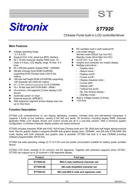
<strong>ST7920</strong>System Block diagramPSBResetCircuitRESI RESO CL1CL2MCLKTimingGeneratorDOUTRSRWEDB4 toDB7DB0 toDB3MPUInterfaceInput/OutputBufferInstructionRegister (IR)InstructionDecoderDataRegister(DR)AddressCounterDisplayData RAM(DDRAM)60 x 16 bits64-bitshiftregister33/49-bit shiftregister64-bitlatchcircuitCommonSignalDriverSegmentSignalDriverLCD DriveVoltageSelectorCOM1 toCOM33SEG1 toSEG64BusyFlagGraphicRAM(GRAM)1024 x 16bitsHalf sizeCharacterROM(HCGROM)1024x16 bitsCharacterGeneratorRAM(CGRAM)1024 bitsCharacterGeneratorROM(CGROM)2M bitsCursorBlinkScrollControllerVssParallel/Serial converterandAttribute CircuitVDDXRESETV0 V1 V2 V3 V4XOFFV3.1 3/42 2003/04/11
<strong>ST7920</strong>Pin coordinatesNo. Name X Y1 V0-2548 18122 V1 -2548 16883 V2 -2548 15624 N.C. -2548 14385 N.C. -2548 13126 N.C. -2548 11887 V3 -2548 10628 V4 -2548 9389 VSS -2548 81210 VDD -2548 68811 XRESET -2548 56212 CL1 -2548 43813 CL2 -2548 31214 VDD -2548 18815 M -2548 6216 DOUT -2548 -6217 RS -2548 -18818 RW -2548 -31219 E -2548 -43820 VSS -2548 -56221 OSC1 -2548 -68822 OSC2 -2548 -81223 PSB -2548 -93824 D0 -2548 -106225 D1 -2548 -118826 D2 -2548 -131227 D3 -2548 -143828 D4 -2548 -156229 D5 -2548 -168830 D6 -2548 -181231 D7 -2306 -193332 XOFF -2181 -193333 VOUT -2056 -193334 CAP3M -1931 -193335 CAP1P -1806 -193336 CAP1M -1681 -193337 CAP2P -1556 -193338 CAP2M -1431 -1933unit: umNo. Name X Y39 VD2 -1306 -193340 C[1] -1181 -193341 C[2] -1056 -193342 C[3] -931 -193343 C[4] -806 -193344 C[5] -681 -193345 C[6] -556 -193346 C[7] -431 -193347 C[8] -306 -193348 C[9] -181 -193349 C[10] -56 -193350 C[11] 69 -193351 C[12] 194 -193352 C[13] 319 -193353 C[14] 444 -193354 C[15] 569 -193355 C[16] 694 -193356 C[17] 819 -193357 C[18] 944 -193358 C[19] 1069 -193359 C[20] 1194 -193360 C[21] 1319 -193361 C[22] 1444 -193362 C[23] 1569 -193363 C[24] 1694 -193364 C[25] 1819 -193365 C[26] 1944 -193366 C[27] 2069 -193367 C[28] 2194 -193368 C[29] 2319 -193369 C[30] 2548 -181270 C[31] 2548 -168871 C[32] 2548 -156272 C[33] 2548 -143873 S[64] 2548 -131274 S[63] 2548 -118875 S[62] 2548 -106276 S[61] 2548 -938V3.1 5/42 2003/04/11
<strong>ST7920</strong>No. Name X Y77 S[60] 2548 -81278 S[59] 2548 -68879 S[58] 2548 -56280 S[57] 2548 -43881 S[56] 2548 -31282 S[55] 2548 -18883 S[54] 2548 -6284 S[53] 2548 6285 S[52] 2548 18886 S[51] 2548 31287 S[50] 2548 43888 S[49] 2548 56289 S[48] 2548 68890 S[47] 2548 81291 S[46] 2548 93892 S[45] 2548 106293 S[44] 2548 118894 S[43] 2548 131295 S[42] 2548 143896 S[41] 2548 156297 S[40] 2548 168898 S[39] 2548 181299 S[38] 2319 1933100 S[37] 2194 1933101 S[36] 2069 1933102 S[35] 1944 1933103 S[34] 1819 1933104 S[33] 1694 1933105 S[32] 1569 1933106 S[31] 1444 1933107 S[30] 1319 1933108 S[29] 1194 1933109 S[28] 1069 1933110 S[27] 944 1933111 S[26] 819 1933112 S[25] 694 1933113 S[24] 569 1933114 S[23] 444 1933115 S[22] 319 1933No. Name X Y116 S[21] 194 1933117 S[20] 69 1933118 S[19] -56 1933119 S[18] -181 1933120 S[17] -306 1933121 S[16] -431 1933122 S[15] -556 1933123 S[14] -681 1933124 S[13] -806 1933125 S[12] -931 1933126 S[11] -1056 1933127 S[10] -1181 1933128 S[9] -1306 1933129 S[8] -1431 1933130 S[7] -1556 1933131 S[6] -1681 1933132 S[5] -1806 1933133 S[4] -1931 1933134 S[3] -2056 1933135 S[2] -2181 1933136 S[1] -2306 1933V3.1 6/42 2003/04/11
<strong>ST7920</strong>Pin DescriptionName No. I/O Connects to FunctionXRESET 11 I ― System reset low activePSB 23 I ―Interface selection:0: serial mode1: 8/4-bits parallel bus modeRS(CS*) 17 I MPURegister select0: select instruction write, busy flag read,address counter read1: select data write, read(Chip select) for serial mode1: chip enable0: chip disableRW(SID*) 18 I MPURead write control0: write1: read(serial data input)E(SCLK*) 19 I MPUEnable trigger(serial clock)D4 to D7 28〜31 I/O MPUHigher nibble data bus for 8 bit interface anddata bus for 4 bit interfaceD0 to D3 24〜27 I/O MPU Lower nibble data bus for 8 bit interfaceCL1 12 O Extension segment drv. Latch signal for extension segment driversCL2 13 O Extension segment drv. Shift clock for extension segment driversM 15 O Extension segment drv.AC signal for extension segment drivers voltageinversionDOUT 16 O Extension segment drv. Data output for extension segment driversCOM1 toCOM3340〜72 O LCD Common signalsSEG1 toSEG64136〜73 O LCD Segment signalsV0 to V41〜3LCD bias voltage――7,8V0 - V4 ≦ 7 VVDD 10,14 I Power VDD : 2.7V to 5.5VVss 9,20 I Power VSS: 0VOSC1, OSC2 21,22 I, O ResistorsFor internal oscillation resistor5.0V R=33K2.7V R=18Kuse OSC1 for external clock inputVOUT 33 O Resistors LCD voltage doubler output*note: The OSC pin must have the shortest wiring pattern of all other pins.To prevent noise from other signal lines , it should also beenclosed with the largest GND pattern possible. Poor noise characteristics on the OSC line will result in malfunction , or adverselyaffect the clock’s duty ratio.V3.1 7/42 2003/04/11
<strong>ST7920</strong>Pin descriptionName No. I/O Connects to DescriptionCAP3MCAP1PCAP1MCAP2M34353638I/O Capacitors Capacitor pins for voltage doublerXOFF 32 O ― Reserved (no connection)CAP2P 37 ― ― Reserved (no connection)VD2 39 I Reference voltage Voltage doubler reference voltageN.C.N.C.N.C.456I―――Test pins (no connection)Note:1. VDD>=V0>=V1>=V2>=V3>=V4 must be maintained2. Two clock options:3.When using voltage doubler for VOUT it is re<strong>com</strong>mended that the total sum of bleeder resistors R1~R5 should be larger than 20K OhmR=33K (VDD=5.0V)R=18K (VDD=2.7V)OSC1 OSC2 OSC1 OSC2RClockexternal resistor & current (VDD=5V)external resistor & Frequency (VDD=5V)Iss (uA)8007006005004003002001000Frequency(KHz)90080070060050040030020010005152540608010015254060801005Resistor(K)Resistor(K)V3.1 8/42 2003/04/11
<strong>ST7920</strong>Voltage doublerVssreference voltage-++-Cap1MCap1PVD2VoutxCap2MCap2PCap3MVout109876543210VoutUnit: V54.74.44.13.83.53.22.92.62.32VD2Reference voltageDoubler voltage mode VD2 & Vout output characteristicNotes:Follower loading resistor total 20k(ohm)Boostaer Cap use 4.7ufPanel size 80mm * 28mm (check display)V3.1 9/42 2003/04/11
<strong>ST7920</strong>Function Description :System interface<strong>ST7920</strong> supports 3 kinds of bus interface to MPU. 8 bits parallel, 4 bits parallel and clock synchronized serialinterface. Parallel interface is selected by PSB=”1” and serial interface by PSB=”0”. 8 bit / 4 bit interface is selectedby function set instruction DL bit.Two 8 bit registers (data register DR, instruction register IR) are used in <strong>ST7920</strong>’s write and read operation. DataRegister(DR)can access DDRAM/CGRAM/GDRAM and IRAM’s data through the address pointer implemented byAddress Counter (AC). Instruction Register (IR) stores the instruction by MPU to <strong>ST7920</strong>.4 modes of read/write operation specified by RS and RW:RS RW descriptionL L MPU write instruction to instruction register(IR)L H MPU read busy flag(BF)and address counter(AC)H L MPU write data to data register(DR)H H MPU read data from data register(DR)Busy Flag(BF)Internal operation is in progress when BF=”1”, <strong>ST7920</strong> is in busy state. No new instruction will be accepted untilBF=”0”. MPU must check BF to determine whether the internal operation is finished and new instruction can be sent.Address counter(AC)Address counter(AC)is used for address pointer of DDRAM/CGRAM/IRAM/GDRAM. (AC) can be set by instruction andafter data read or write to the memories (AC) will increase or decrease by 1 according to the setting in “entry mode set”. WhenRS=“0”and RW=“1”and E=”1” the value of(AC)will output to DB6〜DB0.16x16 character generation ROM (CGROM) and 8x16 half height ROM(HCGROM)<strong>ST7920</strong> provides character generation ROM supporting 8192 16 x 16 character fonts and 126 8 x 16 alphanumericcharacters. It is easy to support multi languages application such as Chinese and English. Two consecutive bytesare used to specify one 16x16 character or two 8x16 half-height characters. Character codes are written intoDDRAM and the corresponding fonts are mapped from CGROM or HCGROM to the display drivers.Character generation RAM (CGRAM)<strong>ST7920</strong> provides RAM to support user-defined fonts. Four sets of 16x16 bit map area are available. Theseuser-defined fonts are displayed the same ways as CGROM fonts through writing character cod data to DDRAM.ICON RAM(IRAM)<strong>ST7920</strong> provides 240 ICON display. It consists of 15 sets of IRAM address. Each IRAM address has 16 bits data.IRAM address should be set first before writing to the IRAM. Two bytes for each address. First higher byte (D15~D8)and then lower byte (D7~D0).V3.1 10/42 2003/04/11
<strong>ST7920</strong>Display data RAM(DDRAM)There are 64x2 bytes for display data RAM area. Can store display data for 16 characters(16x16) by 4 lines or 32characters(8x16) by 4 lines. However, only 2 lines can be displayed at a time. Character codes stored in DDRAMpoint to the fonts specified by CGROM,HCGROM and CGRAM. <strong>ST7920</strong> display half height HCGROM fonts,user-defined CGRAM fonts and full 16x16 CGROM fonts. Data codes 0000H〜0006H are for CGRAMuser-defined fonts. Data codes 02H〜7FH are for half height alpha numeric fonts. Data codes(A140〜D75F)are forBIG5 code and (A1A0〜F7FF) are for GB code.1. display HCGROM fonts:Write 2 bytes data to DDRAM to display two 8x16 fonts. Each byte represents 1character font. The data of each byte is 02H〜7FH.2. display CGRAM fonts:Write 2 bytes data to DDRAM to display one 16x16 font. Only 0000H,0002H,0004H, 0006H are allowed.3. display CGROM fonts:Write 2 bytes data to DDRAM to display one 16x16 font.A140H〜D75FH are for (BIG5) code, A1A0H〜F7FFH are for (GB) code.Higher byte(D15〜D8)are written first and then lower byte(D7〜D0).Refer to Table 5 for address mapCGRAM fonts and CGROM fonts can only be displayed in the start position of each address. (Refer toTable 4)80 81 82 83 84 85 86 87 88 89 8A 8B 8C 8D 8E 8FH L H L H L H L H L H L H L H L H L H L H L H L H L H L H L H LS i t r o n i x S T 7 9 2 0矽 創 電 子 . . 中 文 編 碼 ( 正 確 )矽 創 電 子 . . . 中 文 編 碼Incorrect positionTable 4V3.1 11/42 2003/04/11
<strong>ST7920</strong>Graphic RAM(GDRAM)Graphic display RAM supports 64x256 bits bit-mapped memory space. GDRAM address is set by writing 2consecutive bytes for vertical address and horizontal address. Two-bytes data write to GDRAM for one address.Address counter will automatically increase by one for the next two-byte data. The procedure is as followings.1. Set vertical address(Y)for GDRAM2. Set horizontal address(X)for GDRAM3. Write D15〜D8 to GDRAM 中 (first byte)4. Write D7〜D0 to GDRAM 中 (second byte)Graphic display memory map please refer to Table-8LCD driverLCD driver have 33 <strong>com</strong>mon and 64 segments to drive the LCD panel. Segment data from CGRAM /CGROM/HCGROM are shifted into the 64 bits segment latches to display. Extended segment driver ST7921 can be used toextend the segment drivers to 256.V3.1 12/42 2003/04/11
<strong>ST7920</strong>DDRAM data(char. code)B B BB15~ B4 3 2 1B0B50 X 00 X 000 X 01 X 01CGRAMAddr.B B B B4 3 2 1CGRAM data CGRAM data(higher byte) (lower byte)B D D D D D D D D D D D D D D D D0 1 1 1 1 1 1 9 8 7 6 5 4 3 2 1 05 4 3 2 1 000000000010001 1 0 0 0 0 000011 1 1 1 1 1 10010000000010000100000100010000110001000001 1 1 1 1 1 0010000100100100001000101001 1 1 10010000100011001 10010101001 0 0 00111101001 1001001 0 0 01000001001000101000010010010010000010000101000100100001 0 0 0 0 01011001 1 1 100001 0 0 0 0 011000010010001000000110100000000100000001110000000010000000011110000000000000000000000001 100000001 1 000010001 101000000100001000100001001 1010000110101 1 101 1010010001001000000010100100010101 1 1 1 1 1 10010010001100100000100100100011101 1 1 1 1 1 10010010010000100000100100100100101 1 1 1 1 1 10010010010100100000000100100101101 1 1 1 1 1 1 10 00100110010100000101001001101101 1 1 1 1 1 1001 1 10011101010000010001 0 0 01111000000000000000 0Table 5: DDRAM data(character code), CGRAM data / address mapNote:1. DDRAM data (character code) bit1 and bit2 are the same as CGRAM address bit4 and bit5.2. CGRAM address bit0 to bit3 specify total 16 rows. Row16 is for cursor display. The data in row 16 will be logical OR tothe cursor.3. CGRAM data for each address is 16 bits.4. DDRAM data to select CGRAM bit4 to bit15 must be “0”. Bit0 and bit3 value are “don’t care”.V3.1 13/42 2003/04/11
<strong>ST7920</strong>ICON RAM addressICON RAM dataSet SR ”0”, and then setIRAM address AC3….AC0 Higher byte Lower byteAC3 AC2 AC1 AC0 D15 D14 D13 D12 D11 D10 D9 D8 D7 D6 D5 D4 D3 D2 D1 D00 0 0 0 SEG0 SEG1 SEG2 SEG3 SEG4 SEG5 SEG6 SEG7 SEG8 SEG9 SEG10 SEG11 SEG12 SEG13 SEG14 SEG150 0 0 1 SEG16 SEG17 SEG18 SEG19 SEG20 SEG21 SEG22 SEG23 SEG24 SEG25 SEG26 SEG27 SEG28 SEG29 SEG30 SEG310 0 1 0 SEG32 SEG33 SEG34 SEG35 SEG36 SEG37 SEG38 SEG39 SEG40 SEG41 SEG42 SEG43 SEG44 SEG45 SEG46 SEG470 0 1 1 SEG48 SEG49 SEG50 SEG51 SEG52 SEG53 SEG54 SEG55 SEG56 SEG57 SEG58 SEG59 SEG60 SEG61 SEG62 SEG630 1 0 0 SEG64 SEG65 SEG66 SEG67 SEG68 SEG69 SEG70 SEG71 SEG72 SEG73 SEG74 SEG75 SEG76 SEG77 SEG78 SEG790 1 0 1 SEG80 SEG81 SEG82 SEG83 SEG84 SEG85 SEG86 SEG87 SEG88 SEG89 SEG90 SEG91 SEG92 SEG93 SEG94 SEG950 1 1 0 SEG96 SEG97 SEG98 SEG99 SEG100 SEG101 SEG102 SEG103 SEG104 SEG105 SEG106 SEG107 SEG108 SEG109 SEG110 SEG1110 1 1 1 SEG112 SEG113 SEG114 SEG115 SEG116 SEG117 SEG118 SEG119 SEG120 SEG121 SEG122 SEG123 SEG124 SEG125 SEG126 SEG1271 0 0 0 SEG128 SEG129 SEG130 SEG131 SEG132 SEG133 SEG134 SEG135 SEG136 SEG137 SEG138 SEG139 SEG140 SEG141 SEG142 SEG1431 0 0 1 SEG144 SEG145 SEG146 SEG147 SEG148 SEG149 SEG150 SEG151 SEG152 SEG153 SEG154 SEG155 SEG156 SEG157 SEG158 SEG1591 0 1 0 SEG160 SEG161 SEG162 SEG163 SEG164 SEG165 SEG166 SEG167 SEG168 SEG169 SEG170 SEG171 SEG172 SEG173 SEG174 SEG1751 0 1 1 SEG176 SEG177 SEG178 SEG179 SEG180 SEG181 SEG182 SEG183 SEG184 SEG185 SEG186 SEG187 SEG188 SEG189 SEG190 SEG1911 1 0 0 SEG192 SEG193 SEG194 SEG195 SEG196 SEG197 SEG198 SEG199 SEG200 SEG201 SEG202 SEG203 SEG204 SEG205 SEG206 SEG2071 1 0 1 SEG208 SEG209 SEG210 SEG211 SEG212 SEG213 SEG214 SEG215 SEG216 SEG217 SEG218 SEG219 SEG220 SEG221 SEG222 SEG2231 1 1 0 SEG224 SEG225 SEG226 SEG227 SEG228 SEG229 SEG230 SEG231 SEG232 SEG233 SEG234 SEG235 SEG236 SEG237 SEG238 SEG2391 1 1 1 --- --- --- --- --- --- --- --- --- --- --- --- --- --- --- ---Table 6 ICON RAM address, data and Segment pinsTable 716x8 half-height charactersV3.1 14/42 2003/04/11
<strong>ST7920</strong>GDRAM Vertical address(Y)0123456789101112131415161718192021222324252627282930313233343536373839404142434445464748495051525354555657585960616263GDRAM Horizontal address(X)0 1 ........... 15......................b15 b14 b13...........b0Table 8GDRAM display coordinates and corresponding addressV3.1 15/42 2003/04/11
<strong>ST7920</strong>Instructions<strong>ST7920</strong> offers basic instruction set and extended instruction set:Instruction set 1: (RE=0: basic instruction)codeInsRS RW DB7 DB6 DB5 DB4 DB3 DB2 DB1 DB0DescriptionExec time(540KHZ)CLEAR 0 0 0 0 0 0 0 0 0 1HOME 0 0 0 0 0 0 0 0 1 XFill DDRAM with "20H", and set DDRAM address counter(AC)to "00H"Set DDRAM address counter(AC)to "00H", and put cursorto origin ;the content of DDRAM are not changed1.6 ms72usENTRYMODEDISPLAYON/OFFCURSORDISPLAYCONTROLFUNCTIONSETSETCGRAMADDR.SETDDRAMADDR.READBUSYFLAG(BF)& ADDR.WRITERAMREAD RAM0 0 0 0 0 0 0 1 I/D S0 0 0 0 0 0 1 D C B0 0 0 0 0 1 S/C R/L X X0 0 0 0 1 DL X0REXXSet cursor position and display shift when doing write or readoperationD=1: display ONC=1: cursor ONB=1: blink ONCursor position and display shift control ;the content ofDDRAM are not changedDL=1 8-BIT interfaceDL=0 4-BIT interfaceRE=1: extended instructionRE=0: basic instructionSet CGRAM address to address counter(AC)0 0 0 1 AC5 AC4 AC3 AC2 AC1 AC0 Make sure that in extended instruction SR=0 (scroll orRAM address select)0 0 10AC6AC5 AC4 AC3 AC2 AC1 AC0Set DDRAM address to address counter(AC)AC6 is fixed to 0Read busy flag(BF)for <strong>com</strong>pletion of internal operation, also0 1 BF AC6 AC5 AC4 AC3 AC2 AC1 AC0Read out the value of address counter(AC)1 0 D7 D6 D5 D4 D3 D2 D1 D01 1 D7 D6 D5 D4 D3 D2 D1 D0Write data to internal RAM(DDRAM/CGRAM/IRAM/GDRAM)Read data from internal RAM(DDRAM/CGRAM/IRAM/GDRAM)72us72 us72 us72 us72 us72 us0 us72 us72 usV3.1 16/42 2003/04/11
<strong>ST7920</strong>Instruction set 2: (RE=1: extended instruction)codeInst.RS RW DB7 DB6 DB5 DB4 DB3 DB2 DB1 DB0STAND BY 0 0 0 0 0 0 0 0 0 1SCROLL orRAMADDR.SELECT0 0 0 0 0 0 0 0 1 SRREVERSE 0 0 0 0 0 0 0 1 R1 R0EXTENDEDFUNCTIONSETSETIRAM orSCROLLADDRSETGRAPHICRAMADDR.0 0 0 0 1 DL X1REG 0descriptionEnter stand by mode, any other instruction can terminate(Com1..32 halted, only Com33 ICON can display)SR=1: enable vertical scroll positionSR=0: enable IRAM address (extended instruction)SR=0: enable CGRAM address(basic instruction)Select 1 out of 4 line ( in DDRAM) and decide whether toreverse the display by toggling this instructionR1,R0 initial value is 00DL=1 8-BIT interfaceDL=0 4-BIT interfaceRE=1: extended instruction setRE=0: basic instruction setG=1 :graphic display ONG=0 :graphic display OFFSR=1: AC5~AC0 the address of vertical scroll0 0 0 1 AC5 AC4 AC3 AC2 AC1 AC0SR=0: AC3~AC0 the address of ICON RAM0 0 100Set GDRAM address to address counter(AC)First set vertical address and the horizontal address by0 0 AC3 AC2 AC1 AC0consecutive writingAC5 AC4 AC3 AC2 AC1 AC0Vertical address range AC5...AC0Horizontal address range AC3…AC0Exec. time(540KHZ)72 us72 us72 us72 us72 us72 usNote:1. Make sure that <strong>ST7920</strong> is not in busy state by reading the busy flag before sending instruction or data. If use delay loopinstead please make sure the delay time is enough. Please refer to the instruction execution time.2. “RE”is the selection bit of basic and extended instruction set. Each time when altering the value of RE it will remain.There is no need to set RE every time when using the same group of instruction set.V3.1 17/42 2003/04/11
<strong>ST7920</strong>Initial setting(Register flag) (RE=0: basic instruction)codeInst.RS RW DB7 DB6 DB5 DB4 DB3 DB2 DB1 DB0DescriptionENTRY0 0 0 0 0 0 0 1 I/D SMODE SET1 0Cursor move to right ,DDRAM address counter(AC)plus 1DISPLAYSTATUS0 0 0 0 0 0 1 D C B0 0 0Display, cursor and blink ALL OFFCURSOR 0 0 0 0 0 1 S/C R/L X XDISPLAYSHIFT X XNo cursor or display shift operationFUNCTIONSET00 0 0 0 1 DL XRE1 0XX8 BIT MPU interface , basic instruction setInitial setting(Register flag) (RE=1: extended instruction set)codeInst.RS RW DB7 DB6 DB5 DB4 DB3 DB2 DB1 DB0SCROLL ORRAMADDR.SELECT0 0 0 0 0 0 0 0 1 SR0descriptionAllow IRAMaddress or set CGRAM addressREVERSE0 0 0 0 0 0 0 1 R1 R00 0Begin with normal and toggle to reverse1EXTENDED 0 0 0 0 1 DL XREFUNCTIONG 0SET 0Graphic display OFFV3.1 18/42 2003/04/11
<strong>ST7920</strong>Description of basic instruction set• CLEARRSRWDB7DB6DB5DB4DB3DB2DB1DB0Code0000000001Fill DDRAM with "20H"(space code). And set DDRAM address counter (AC)to"00H". Set entry mode I/D bit to be "1".Cursor moves right and AC adds 1 after write or read operation.• HOMERSRWDB7DB6DB5DB4DB3DB2DB1DB0Code000000001xSet DDRAM address counter(AC)to "00H". Cursor moves to origin. Then content of DDRAM is not changed.• ENTRY MODE SETRSRWDB7DB6DB5DB4DB3DB2DB1 DB0Code00000001I/DSSet the cursor movement and display shift direction when doing write or read operation.I/D :address counter increase / decreaseWhen I/D = "1", cursor moves right, DRAM address counter(AC)add by 1.When I/D = "0", cursor moves left, DRAM address counter(AC)subtract by 1.S: Display shiftS I/D DESCRIPTIONH H Entire display shift left by 1H L Entire display shift right by 1V3.1 19/42 2003/04/11
<strong>ST7920</strong>• DISPLAY STATUSRSRWDB7DB6DB5DB4DB3DB2DB1DB0Code0000001DCBControls display, cursor and blink ON/OFF.D : Display ON/OFF control bitWhen D = "1", display ONWhen D = "0",display OFF , the content of DDRAM is not changedC : Cursor ON/OFF control bitWhen C = "1", cursor ON.When C = "0", cursor OFF.B : Blink ON/OFF control bitWhen B = "1", cursor position blink ON. Then display data in cursor position will blink.When B = "0", cursor position blink OFF• CURSOR AND DISPLAY SHIFT CONTROLRSRWDB7DB6DB5DB4DB3DB2DB1 DB0Code000001S/CR/LxxInstruction to move the cursor or shift the entire display. The content of DDRAM is not changed.S/C R/L Description AC ValueL L Cursor moves left by 1 AC=AC-1L H Cursor moves right by 1 AC=AC+1H L Display shift left by 1, cursor also follows to shift. AC=ACH H Display shift right by 1, cursor also follows to shift. AC=ACV3.1 20/42 2003/04/11
<strong>ST7920</strong>• FUNCTION SETRS RW DB7 DB6 DB5 DB4DB3DB2DB1DB0Code0 0 0 0 1 DL X RExxDL : 4/8 BIT interface control bitWhen DL = "1", 8 BIT MPU bus interfaceWhen DL = "0", 為 4 BIT MPU bus interfaceRE : extended instruction set control bitWhen RE = "1", extended instruction setWhen RE = "0", basic instruction setIn same instruction cannot alter DL and RE at once. Make sure that change DL first then RE.• SET CGRAM ADDRESSRS RW DB7 DB6 DB5 DB4 DB3 DB2 DB1DB00 0 0 1 AC5 AC4 AC3 AC2AC1AC0CodeSet CGRAM address to address counter(AC)AC range is 00H..3FHMake sure that in extended instruction SR=0 (scroll address or RAM address select)• SET DDRAM ADDRESSRS RW DB7 DB6 DB5 DB4 DB3 DB2 DB1DB00 0 1 AC6 AC5 AC4 AC3 AC2AC1AC0CodeSet DDRAM address to address counter(AC).First line AC range is 80H..8FHSecond line AC range is 90H..9FHThird line AC range is A0H..AFHFourth line AC range is B0H..BFHPlease note that only 2 lines can be display at a time.• READ BUSY FLAG(BF)AND ADDRESSRS RW DB7 DB6 DB5 DB4 DB3 DB2 DB1DB00 1 BF AC6 AC5 AC4 AC3 AC2AC1AC0CodeRead busy flag(BF)can check whether internal operation is finished. At the same time the value of address counterV3.1 21/42 2003/04/11
<strong>ST7920</strong>(AC)is also read. When BF = “1” new instruction will not be accepted. Must wait for BF = “0” for new instruction.• WRITE DATA TO RAMRSRWDB7DB6DB5DB4DB3DB2DB1DB0Code10D7D6D5D4D3D2D1D0Write data to internal RAM and alter the (AC) by 1Each RAM address (CGRAM,DDRAM,IRAM…..) must write 2 consecutive bytes for 16 bit data. After the secondbyte the address counter will add or subtract by 1 according to the entry mode set control bit.• READ RAM DATARSRWDB7DB6DB5DB4DB3DB2DB1 DB0Code11D7D6D5D4D3D2D1D0Read data from internal RAM and alter the (AC) by 1After address set to read (CGRAM,DDRAM,IRAM…..)a DUMMY READ is required.There is no need to DUMMY READ for the following bytes unless a new address set instruction is issued.V3.1 22/42 2003/04/11
<strong>ST7920</strong>Description of extended instruction set• STAND BYRSRWDB7DB6DB5DB4DB3DB2DB1DB0Code0000000001Instruction to enter stand by mode. Any other instruction follows this instruction can terminate stand by.The content of DDRAM remain the same.• VERTICAL SCROLL OR RAM ADDRESS SELECTRSRWDB7DB6DB5DB4DB3DB2DB1DB0Code000000001SRWhen SR = "1", the vertical scroll address set is enabled.When SR = "0", the IRAM address set (extended instruction) and CGRAM address set(basic instruction) is enabled.• REVERSERSRWDB7DB6DB5DB4DB3DB2DB1 DB0Code00000001R1R0Select 1 out of 4 lines to reverse the display and to toggle the reverse condition by repeating this instruction.R1,R0 initial vale is 00. When set the first time the display is reversed and set the second time the display be<strong>com</strong>e normal.R1 R0 DescriptionL L First line normal or reverseL H Second line normal or reverseH L Third line normal or reverseH H Fourth line normal or reversePlease note that only 2 lines out of 4 line display data can be displayed.V3.1 23/42 2003/04/11
<strong>ST7920</strong>• EXTENED FUNCTION SETRS RW DB7 DB6 DB5 DB4DB3DB2DB1DB0Code0 0 0 0 1 DL x REGxDL : 4/8 BIT interface control bitWhen DL = "1", 8 BIT MPU interfaceWhen DL = "0", 4 BIT MPU interfaceRE : extended instruction set control bitWhen RE = "1", extended instruction setWhen RE = "0", basic instruction setG : Graphic display control bitWhen G = "1", graphic display ONWhen G = "0", Graphic display OFFIn same instruction cannot alter DL, RE and G at once. Make sure that change DL or G first and then RE.• SET IRAM OR SCROLL ADDRESSRS RW DB7 DB6 DB5 DB4 DB3 DB2 DB1DB00 0 0 1 AC5 AC4 AC3 AC2CodeSR=1: AC5~AC0 is vertical scroll displacement addressSR=0: AC3~AC0 is ICON RAM address• SET GRAPHIC RAM ADDRESSAC1AC0RS RW DB7 DB6 DB5 DB4 DB3 DB2 DB1DB00 0 1 0 AC5 AC4 AC3 AC2AC1AC0CodeSet GDRAM address to address counter(AC).First set vertical address and then horizontal address(write 2 consecutive bytes to <strong>com</strong>plete vertical and horizontal address set)Vertical address range is AC5...AC0Horizontal address range is AC3…AC0The address counter(AC)of graphic RAM(GRAM) only increment after write for horizontal address. After horizontal address=0FH it will automatically back to 00H. However, the vertical address will not increase as the result of the same action.V3.1 24/42 2003/04/11
<strong>ST7920</strong>Serial interface :<strong>ST7920</strong> is in serial interface mode when pull down PSB pin. Two pins (SCLK and SID) are used to <strong>com</strong>plete the data transfer.Only write data is available.When connecting several <strong>ST7920</strong>, chip select(CS)must be used. Only when(CS)is high the serial clock(SCLK)can beaccepted. On the other hand, when chip select(CS)is low <strong>ST7920</strong> serial counter and data will be reset. Transmission will beterminated and data will be cleared. Serial transfer counter is set to the first bit. For a minimal system with only one <strong>ST7920</strong> andone MPU, only SCLK and SID pins are necessary. CS pin should pull to high.<strong>ST7920</strong>’s serial clock(SCLK)is asynchronous to the internal clock and is generated by MPU. When multiple instruction/data istransferred instruction execution time must be considered. Must wait for the previous instruction to finish before sending thenext. <strong>ST7920</strong> has no internal instruction buffer area.When starting a transmission a start byte is required. It consists of 5 consecutive 〝1〞(sync character). Serial transfer counterwill be reset and synchronized. Following 2 bits for read/write(RW)and register/data select(RS). Last 4 bits is filled by 〝0〞。After receiving the sync character and RW and RS bits, every 8 bits instruction/data will be separated into 2 groups. Higher4 bits(DB7~DB4)will be placed in first section followed by 4 〝0〞. And lower 4 bits(DB3~DB0)will be placed in secondsection followed by 4 〝0〞.CSSCLK1 2 3 4 5 6 7 8 9 10 11 12 13 14 15 16 17 18 19 20 21 22 23 24SID1 1 1 1 1 RW RS 0 D7 D6 D5 D4 0 0 0 0 D3 D2 D1 D0 0 0 0 0SynchronizingBit stringHigherdataLowerdata1 st byte 2 nd byteTiming Diagram of Serial Mode Data TransferV3.1 26/42 2003/04/11
<strong>ST7920</strong>8051 demo program for serial interface;--------------------------------------------------------------; Write data from A into INSTRUCTION Register;--------------------------------------------------------------WRINS:SETB CSSETB SID ; SID = 1CLR SCLKSETB SCLK ; READ DATA FROM SIDCLR SCLKSETB SCLK ; READ DATA FROM SIDCLR SCLKSETB SCLK ; READ DATA FROM SIDCLR SCLKSETB SCLK ; READ DATA FROM SIDCLR SCLKSETB SCLK ; READ DATA FROM SIDCLR SCLKCLR SID ; SID = 0SETB SCLK ; READ DATA FROM SIDCLR SCLKSETB SCLK ; READ DATA FROM SIDCLR SCLKSETB SCLK ; READ DATA FROM SIDCLR SCLKMOVBIT SID, A.7 ; SID = A.7SETB SCLK ; READ DATA FROM SIDCLR SCLKMOVBIT SID, A.6 ; SID = A.6SETB SCLK ; READ DATA FROM SIDCLR SCLKMOVBIT SID, A.5 ; SID = A.5SETB SCLK ; READ DATA FROM SIDCLR SCLKMOVBIT SID, A.4 ; SID = A.4SETB SCLK ; READ DATA FROM SIDCLR SCLKCLR SID ; SID = 0SETB SCLK ; READ DATA FROM SIDCLR SCLKSETB SCLK ; READ DATA FROM SIDCLR SCLKSETB SCLK ; READ DATA FROM SIDCLR SCLKSETB SCLK ; READ DATA FROM SIDCLR SCLKMOVBIT SID, A.3 ; SID = A.3SETB SCLK ; READ DATA FROM SIDCLR SCLKMOVBIT SID, A.2 ; SID = A.2SETB SCLK ; READ DATA FROM SIDCLR SCLKMOVBIT SID, A.1 ; SID = A.1SETB SCLK ; READ DATA FROM SIDCLR SCLKMOVBIT SID, A.0 ; SID = A.0SETB SCLK ; READ DATA FROM SIDCLR SCLKCLR SID ; SID = 0SETB SCLK ; READ DATA FROM SIDCLR SCLKSETB SCLK ; READ DATA FROM SIDCLR SCLKSETB SCLK ; READ DATA FROM SIDCLR SCLKSETB SCLK ; READ DATA FROM SIDCLR SCLKCLR CSCALL DLY8RET;-------------------------------------------------; Write data from A into DATA Register;-------------------------------------------------WRDATA:SETB CSSETB SID ; SID = 1CLR SCLKSETB SCLK ; READ DATA FROM SIDCLR SCLKSETB SCLK ; READ DATA FROM SIDCLR SCLKSETB SCLK ; READ DATA FROM SIDCLR SCLKSETB SCLK ; READ DATA FROM SIDCLR SCLKSETB SCLK ; READ DATA FROM SIDCLR SCLKCLR SID ; SID = 0SETB SCLK ; READ DATA FROM SIDCLR SCLKSETB SID ; SID = 1SETB SCLK ; READ DATA FROM SIDCLR SCLKCLR SID ; SID = 0SETB SCLK ; READ DATA FROM SIDCLR SCLKMOVBIT SID, A.7 ; SID = A.7SETB SCLK ; READ DATA FROM SIDCLR SCLKMOVBIT SID, A.6 ; SID = A.6SETB SCLK ; READ DATA FROM SIDCLR SCLKMOVBIT SID, A.5 ; SID = A.5SETB SCLK ; READ DATA FROM SIDCLR SCLKMOVBIT SID, A.4 ; SID = A.4SETB SCLK ; READ DATA FROM SIDCLR SCLKCLR SID ; SID = 0SETB SCLK ; READ DATA FROM SIDCLR SCLKSETB SCLK ; READ DATA FROM SIDCLR SCLKSETB SCLK ; READ DATA FROM SIDCLR SCLKSETB SCLK ; READ DATA FROM SIDCLR SCLKMOVBIT SID, A.3 ; SID = A.3SETB SCLK ; READ DATA FROM SIDCLR SCLKMOVBIT SID, A.2 ; SID = A.2SETB SCLK ; READ DATA FROM SIDCLR SCLKMOVBIT SID, A.1 ; SID = A.1SETB SCLK ; READ DATA FROM SIDCLR SCLKMOVBIT SID, A.0 ; SID = A.0SETB SCLK ; READ DATA FROM SIDCLR SCLKCLR SID ; SID = 0SETB SCLK ; READ DATA FROM SIDCLR SCLKSETB SCLK ; READ DATA FROM SIDCLR SCLKSETB SCLK ; READ DATA FROM SIDCLR SCLKSETB SCLK ; READ DATA FROM SIDCLR SCLKCLR CSCALL DLY8RETV3.1 27/42 2003/04/11
<strong>ST7920</strong>8 bit interface:POWER ONWait time >40msXRESET LOW HIGHFunction setRS R/W DB7 DB6 DB5 DB4 DB3 DB2 DB1 DB00 0 0 0 1 1 X 0 X XWait time >100uSFunction setRS R/W DB7 DB6 DB5 DB4 DB3 DB2 DB1 DB00 0 0 0 1 1 X 0 X XWait time >37uSDisplay ON/OFF controlRS R/W DB7 DB6 DB5 DB4 DB3 DB2 DB1 DB00 0 0 0 0 0 1 D C BWait time >100uSDisplay clearRS R/W DB7 DB6 DB5 DB4 DB3 DB2 DB1 DB00 0 0 0 0 0 0 0 0 1Wait time >10mSEntry mode setRS R/W DB7 DB6 DB5 DB4 DB3 DB2 DB1 DB00 0 0 0 0 0 0 1 I/D SInitialization endV3.1 28/42 2003/04/11
<strong>ST7920</strong>4 bit interface:POWER ONWait time >40msXRESET LOW HIGHFunction setRS R/W DB7 DB6 DB5 DB4 DB3 DB2 DB1 DB00 0 0 0 1 0 X X X XWait time >100uSFunction setRS R/W DB7 DB6 DB5 DB4 DB3 DB2 DB1 DB00 0 0 0 1 0 X X X X0 0 X 0 X X X X X XWait time >100uSDisplay ON/OFF controlRS R/W DB7 DB6 DB5 DB4 DB3 DB2 DB1 DB00 0 0 0 0 0 X X X X0 0 1 D C B X X X XWait time >100uSDisplay clearRS R/W DB7 DB6 DB5 DB4 DB3 DB2 DB1 DB00 0 0 0 0 0 X X X X0 0 0 0 0 1 X X X XWait time >10mSEntry mode setRS R/W DB7 DB6 DB5 DB4 DB3 DB2 DB1 DB00 0 0 0 0 0 X X X X0 0 0 1 I/D S X X X XInitialization endV3.1 29/42 2003/04/11
<strong>ST7920</strong>Built in voltage boosterVoutVssVDD5.4V-++-Cap1MCap1PVD2參 考 電 壓VD22.7VxCap2MCap2PVoutCap3MVoutVssExternal reset timingVDDTresXRESETTrwXRESET pulse width Trw 10usRESET start time Tres 50nsV3.1 30/42 2003/04/11
<strong>ST7920</strong>LCD driving wave form (1/33 duty , 1/5 bias )When oscillation frequency is 540KHZ, 1 clock cycle time = 1.85us1 frame = 1.85us x 300 x 33 = 18315us=18.3ms300 clocks1 2 3 4 33 1 2 3 4 33 1 2 3 4 33COM1V0V1V2V3V4VSSCOM2V0V1V2V3V4VSSCOM33V0V1V2V3V4VSSSEGxoffV0V1V2V3V4VSSSEGxonV0V1V2V3V4VSS1 frameV3.1 31/42 2003/04/11
<strong>ST7920</strong>Absolute Maximum RatingsCharacteristics Symbol ValuePower Supply Voltage V DD -0.3V to +5.5VLCD Driver Voltage V LCD -0.3V to +7.0VInput Voltage V IN -0.3V to V DD +0.3VOperating Temperature T A -20 o C to + 85 o CStorage Temperature T STO -55 o C to + 125 o CDC Characteristics ( T A = 25 o C , V DD = 2.7 V – 4.5 V )Symbol Characteristics Test Condition Min. Typ. Max. UnitV DD Operating Voltage - 2.7 - 5.5 VV LCD LCD Voltage V0-V SS 3.0 - 7 VI CCV IH1V IL1V IH2V IL2V OH1V OL1V OH2V OL2Power Supply Current f OSC = 530KHz, V DD =3.0VRf=18KΩ- 0.20 0.45 mAInput High Voltage- 0.7V DD - V DD V(Except OSC1)Input Low Voltage- - 0.3 - 0.6 V(Except OSC1)Input High Voltage- V DD –1 - V DD V(OSC1)Input Low Voltage- - - 1.0 V(OSC1)Output High Voltage I OH = -0.1mA 0.8V DD - V DD V(DB0 - DB7)Output Low Voltage I OL = 0.1mA - - 0.1 V(DB0 - DB7)Output High Voltage(Except DB0 - DB7)I OH = -0.04mA 0.8V DD - V DD VOutput Low Voltage I OL = 0.04mA - - 0.1V DD V(Except DB0 - DB7)I LEAK Input Leakage Current V IN = 0V to V DD -1 - 1 µAI PUP Pull Up MOS Current V DD = 3V 22 27 32 µAV3.1 32/42 2003/04/11
<strong>ST7920</strong>DC Characteristics ( T A = 25 o C, V DD = 4.5 V - 5.5 V )Symbol Characteristics Test Condition Min. Typ. Max. UnitV DD Operating Voltage - 4.5 - 5.5 VV LCD LCD Voltage V0-V SS 3.0 - 7 VI CC Power Supply Current f OSC = 540KHz, V DD =5VRf=33KΩ- 0.45 0.75 mAV IH1V IL1V IH2V IL2V OH1V OL1V OH2V OL2Input High Voltage(Except OSC1)- 0.7V DD - V DD VInput Low Voltage- -0.3 - 0.6 V(Except OSC1)Input High Voltage- V DD -1 - V DD V(OSC1)Input Low Voltage- - - 1.0 V(OSC1)Output High Voltage I OH = -0.1mA 0.8V DD - V DD V(DB0 - DB7)Output Low Voltage I OL = 0.1mA - - 0.4 V(DB0 - DB7)Output High Voltage I OH = -0.04mA 0.8V DD - V DD V(Except DB0 - DB7)Output Low Voltage I OL = 0.04mA - - 0.1V DD V(Except DB0 - DB7)I LEAK Input Leakage Current V IN = 0V to V DD -1 - 1 µAI PUP Pull Up MOS Current V DD = 5V 75 80 85 µAV3.1 33/42 2003/04/11
<strong>ST7920</strong>AC Characteristics (T A = 25 o C, V DD = 4.5V) Parallel Mode InterfaceSymbol Characteristics Test Condition Min. Typ. Max. UnitInternal Clock Operationf OSC OSC Frequency R = 33KΩ 480 540 600 KHzExternal Clock Operationf EX External Frequency - 480 540 600 KHzDuty Cycle - 45 50 55 %T R ,T F Rise/Fall Time - - - 0.2 µsWrite Mode (Writing data from MPU to <strong>ST7920</strong>)T C Enable Cycle Time Pin E 1200 - - nsT PW Enable Pulse Width Pin E 140 - - nsT R ,T F Enable Rise/Fall Time Pin E - - 25 nsT AS Address Setup Time Pins: RS,RW,E 10 - - nsT AH Address Hold Time Pins: RS,RW,E 20 - - nsT DSW Data Setup Time Pins: DB0 - DB7 40 - - nsT H Data Hold Time Pins: DB0 - DB7 20 - - nsRead Mode (Reading Data from <strong>ST7920</strong> to MPU)T C Enable Cycle Time Pin E 1200 - - nsT PW Enable Pulse Width Pin E 140 - - nsT R ,T F Enable Rise/Fall Time Pin E - - 25 nsT AS Address Setup Time Pins: RS,RW,E 10 - - nsT AH Address Hold Time Pins: RS,RW,E 20 - - nsT DDR Data Delay Time Pins: DB0 - DB7 - - 100 nsT H Data Hold Time Pins: DB0 - DB7 20 - - nsInterface Mode with LCD Driver(ST7921)T CWH Clock Pulse with High Pins: CL1, CL2 800 - - nsT CWL Clock Pulse with Low Pins: CL1, CL2 800 - - nsT CST Clock Setup Time Pins: CL1, CL2 500 - - nsT SU Data Setup Time Pin: D 300 - - nsT DH Data Hold Time Pin: D 300 - - nsT DM M Delay Time Pin: M -1000 - 1000 nsV3.1 34/42 2003/04/11
<strong>ST7920</strong>AC Characteristics (T A = 25 o C, V DD = 2.7V) Parallel Mode InterfaceSymbol Characteristics Test Condition Min. Typ. Max. UnitInternal Clock Operationf OSC OSC Frequency R = 18KΩ 470 530 590 KHzExternal Clock Operationf EX External Frequency - 470 530 590 KHzDuty Cycle - 45 50 55 %T R ,T F Rise/Fall Time - - - 0.2 µsWrite Mode (Writing data from MPU to <strong>ST7920</strong>)T C Enable Cycle Time Pin E 1800 - - nsT PW Enable Pulse Width Pin E 160 - - nsT R ,T F Enable Rise/Fall Time Pin E - - 25 nsT AS Address Setup Time Pins: RS,RW,E 10 - - nsT AH Address Hold Time Pins: RS,RW,E 20 - - nsT DSW Data Setup Time Pins: DB0 - DB7 40 - - nsT H Data Hold Time Pins: DB0 - DB7 20 - - nsRead Mode (Reading Data from <strong>ST7920</strong> to MPU)T C Enable Cycle Time Pin E 1800 - - nsT PW Enable Pulse Width Pin E 320 - - nsT R ,T F Enable Rise/Fall Time Pin E - - 25 nsT AS Address Setup Time Pins: RS,RW,E 10 - - nsT AH Address Hold Time Pins: RS,RW,E 20 - - nsT DDR Data Delay Time Pins: DB0 - DB7 - - 260 nsT H Data Hold Time Pins: DB0 - DB7 20 - - nsInterface Mode with LCD Driver(ST7921)T CWH Clock Pulse with High Pins: CL1, CL2 800 - - nsT CWL Clock Pulse with Low Pins: CL1, CL2 800 - - nsT CST Clock Setup Time Pins: CL1, CL2 500 - - nsT SU Data Setup Time Pin: D 300 - - nsT DH Data Hold Time Pin: D 300 - - nsT DM M Delay Time Pin: M -1000 - 1000 nsV3.1 35/42 2003/04/11
<strong>ST7920</strong>8 bit interface timing diagram• MPU write data to <strong>ST7920</strong>RSVIH1VIL1TASTAHR/WTPWTAHEDB0-DB7TRTDSWValid dataTHTC• MPU read data from <strong>ST7920</strong>RSR/WEDB0-DB7VIH1VIL1TRTASTDDRTPWValid dataTAHTAHTHTCV3.1 36/42 2003/04/11
<strong>ST7920</strong>AC Characteristics (T A = 25 o C, V DD = 4.5V) Serial Mode InterfaceSymbol Characteristics Test Condition Min. Typ. Max. UnitInternal Clock Operationf OSC OSC Frequency R = 33KΩ 470 530 590 KHzExternal Clock Operationf EX External Frequency - 470 530 590 KHzDuty Cycle - 45 50 55 %T R ,T F Rise/Fall Time - - - 0.2 µsTSCYC Serial clock cycle Pin E 400 - - nsTSHW SCLK high pulse width Pin E 200 - - nsTSLW SCLK low pulse width Pin E 200 - - nsTSDS SID data setup time Pins RW 40 - - nsTSDH SID data hold time Pins RW 40 - - nsTCSS CS setup time Pins RS 60 - - nsTCSH CS hold time Pins RS 60 - - nsAC Characteristics (T A = 25 o C, V DD = 2.7V) Serial Mode InterfaceSymbol Characteristics Test Condition Min. Typ. Max. UnitInternal Clock Operationf OSC OSC Frequency R = 18KΩ 470 530 590 KHzExternal Clock Operationf EX External Frequency - 470 530 590 KHzDuty Cycle - 45 50 55 %T R ,T F Rise/Fall Time - - - 0.2 µsTSCYC Serial clock cycle Pin E 600 - - nsTSHW SCLK high pulse width Pin E 300 - - nsTSLW SCLK low pulse width Pin E 300 - - nsTSDS SID data setup time Pins RW 40 - - nsTSDH SID data hold time Pins RW 40 - - nsTCSS CS setup time Pins RS 60 - - nsTCSH CS hold time Pins RS 60 - - nsV3.1 37/42 2003/04/11
<strong>ST7920</strong>Serial interface timing diagram• MPU write data to <strong>ST7920</strong>CSTCSSTCSHTSCYCSCLKTfTSLWTSDSTrTSHWTSDHSIDValid dataV3.1 38/42 2003/04/11
<strong>ST7920</strong>I/O pin diagramInput PAD: E (No Pull-up)Input PAD: RS, RW(with Pull-up)Output PAD: CL1, CL2, M, DEnableDATAI/O PAD: DB0 – DB7V3.1 39/42 2003/04/11
<strong>ST7920</strong>V3.1 40/42 2003/04/11Application circuit 1:LCD: 32 COM x 160 SEGLCD Voltage : VCC1 2 3 4 5 6ABCD654321DCBATitleNumberRevisionSizeBDate: 1-Mar-2001 Sheet ofFile: D:\Buffer-2\7920V1.DDB Drawn By:V01V12V23VXA4VXB5VXC6V37V48VSS9VDD10XRESET11CL112CL213VDD14M15DOUT16RS17RW18E19VSS20OSC121OSC222PSB23D024D125D226D327D428D529D630D731XOFF32VOUT33CAP3M34CAP1P35CAP1M36CAP2P37CAP2M38VD239C140C241C342C443C544C645C746C847C948C1049C1150C1251C1352C1453C1554C1655C1756C1857C1958C2059C2160C2261C2362C2463C2564C2665C2766C2867C2968C3069C3170C3271C3372S6473S6374S6275S6176S6077S5978S5879S5780S5681S5582S5483S5384S5285S5186S5087S4988S4889S4790S4691S4592S4493S4394S4295S4196S4097S3998S3899S37100S36101S35102S34103S33104S32105S31106S30107S29108S28109S27110S26111S25112S24113S23114S22115S21116S20117S19118S18119S17120S16121S15122S14123S13124S12125S11126S10127S9128S8129S7130S6131S5132S4133S3134S2135S1136U1<strong>ST7920</strong>S501S512S523S534S545S556S567S578S589S5910S6011S6112S6213S6314S6415S6516S6617S6718S6819S6920S7021S7122S7223S7324S7425S7526S7627S7728S7829S7930S8031S8132S8233S8334S8435S8536S8637S8738S8839S8940S9041S9142S9243S9344S9445S9546S9647S4848S4749S4650S4551S4452S4353S4254S4155S4056S3957S3858S3759S3660S3561S3462S3363S3264S3165S3066S2967S2868S2769S2670S2571S2472S2373S2274S2175S2076S1977S1878S1779S1680S1581S1482S1383S1284S1185S1086S987S888S789S690S591S492S393S294S195V096V297V398VSS99VDD100CL1101SHL1102SHL2103CL2104DL1105DR1106DL2107DR2108M109S49110U2ST7921C81C72C63C54C45C36C27C18S19S210S311S412S513S614S715S816S917S1018S1119S1220S1321S1422S1523S1624S1725S1826S1927S2028S4129S4230S4331S4432S4533S4634S4735S4836S4937S5038S5139S5240S5341S5442S5543S5644S5745S5846S5947S6048S8149S8250S8351S8452S8553S8654S8755S8856S8957S9058S9159S9260S9361S9462S9563S9664S9765S9866S9967S10068S12169S12270S12371S12472S12573S12674S12775S12876S12977S13078S13179S13280S13381S13482S13583S13684S13785S13886S13987S14088C1789C1890C1991C2092C2193C2294C2395C2496C997C1098C1199C12100C13101C14102C15103C16104S21105S22106S23107S24108S25109S26110S27111S28112S29113S30114S31115S32116S33117S34118S35119S36120S37121S38122S39123S40124S61125S62126S63127S64128S65129S66130S67131S68132S69133S70134S71135S72136S73137S74138S75139S76140S77141S78142S79143S80144S101145S102146S103147S104148S105149S106150S107151S108152S109153S110154S111155S112156S113157S114158S115159S116160S117161S118162S119163S120164S141165S142166S143167S144168S145169S146170S147171S148172S149173S150174S151175S152176S153177S154178S155179S156180S157181S158182S159183S160184C32185C31186C30187C29188C28189C27190C26191C25192L1WDG1603PC110412345678910111213141516JP1HEADER 1612JACON212JKCON2123J1CON3R14.7KR24.7KR32.2KR44.7KR54.7KR633KR72KR933R833VCCVCCVCCVCC12JP2HEADER 2VCCVCCC1C2C3C4C5C6C7C8C9C10C11C12C13C14C15C16C17C18C19C20C21C22C23C24C25C26C27C28C29C30C31C32S39S40S41S42S43S44S45S46S47S48S49S50S51S52S53S54S55S56S57S58S59S60S61S62S63S64S1S2S3S4S5S6S7S8S9S10S11S12S13S14S15S16S17S18S19S20S21S22S23S24S25S26S27S28S29S30S31S32S33S34S35S36S37S38S65S66S67S68S69S70S71S72S73S74S75S76S77S78S79S80S81S82S83S84S85S86S87S88S89S90S91S92S93S94S95S96S97S98S99S100S101S102S103S104S105S106S107S108S109S110S111S112S113S114S115S116S117S118S119S120S121S122S123S124S125S126S127S128S129S130S131S132S133S134S135S136S137S138S139S140S141S142S143S144S145S146S147S148S149S150S151S152S153S154S155S156S157S158S159S160C25C26C27C28C29C30C31C32C1C2C3C4C5C6C7C8C9C10C11C12C13C14C15C16C17C18C19C20C21C22C23C24S1S2S3S4S5S6S7S8S9S10S11S12S13S14S15S16S17S18S19S20S21S22S23S24S25S26S27S28S29S30S31S32S33S34S35S36S37S38S39S40S41S42S43S44S45S46S47S48S49S50S51S52S53S54S55S56S57S58S59S60S61S62S63S64S65S66S67S68S69S70S71S72S73S74S75S76S77S78S79S80S81S82S83S84S85S86S87S88S89S90S91S92S93S94S95S96S97S98S99S100S101S102S103S104S105S106S107S108S109S110S111S112S113S114S115S116S117S118S119S120S121S122S123S124S125S126S127S128S129S130S131S132S133S134S135S136S137S138S139S140S141S142S143S144S145S146S147S148S149S150S151S152S153S154S155S156S157S158S159S160Paul Yung1 11.2Sitronix<strong>ST7920</strong> LCMR1010K
<strong>ST7920</strong>V3.1 41/42 2003/04/11Application circuit 2:LCD: 32 COM x 160 SEGLCD Voltage : VCC x 2(Voltage doubler is used)*Vlcd should not over 7v.1 2 3 4 5 6ABCD654321DCBATitleNumberRevisionSizeBDate: 17-Aug-2001 Sheet ofFile:D:\adom\Documents\sch\7920_B~13.DDB Drawn By:V01V12V23VXA4VXB5VXC6V37V48VSS9VDD10XRESET11CL112CL213VDD14M15DOUT16RS17RW18E19VSS20OSC121OSC222PSB23D024D125D226D327D428D529D630D731XOFF32VOUT33CAP3M34CAP1P35CAP1M36CAP2P37CAP2M38VD239C140C241C342C443C544C645C746C847C948C1049C1150C1251C1352C1453C1554C1655C1756C1857C1958C2059C2160C2261C2362C2463C2564C2665C2766C2867C2968C3069C3170C3271C3372S6473S6374S6275S6176S6077S5978S5879S5780S5681S5582S5483S5384S5285S5186S5087S4988S4889S4790S4691S4592S4493S4394S4295S4196S4097S3998S3899S37100S36101S35102S34103S33104S32105S31106S30107S29108S28109S27110S26111S25112S24113S23114S22115S21116S20117S19118S18119S17120S16121S15122S14123S13124S12125S11126S10127S9128S8129S7130S6131S5132S4133S3134S2135S1136U1<strong>ST7920</strong>S501S512S523S534S545S556S567S578S589S5910S6011S6112S6213S6314S6415S6516S6617S6718S6819S6920S7021S7122S7223S7324S7425S7526S7627S7728S7829S7930S8031S8132S8233S8334S8435S8536S8637S8738S8839S8940S9041S9142S9243S9344S9445S9546S9647S4848S4749S4650S4551S4452S4353S4254S4155S4056S3957S3858S3759S3660S3561S3462S3363S3264S3165S3066S2967S2868S2769S2670S2571S2472S2373S2274S2175S2076S1977S1878S1779S1680S1581S1482S1383S1284S1185S1086S987S888S789S690S591S492S393S294S195V096V297V398VSS99VDD100CL1101SHL1102SHL2103CL2104DL1105DR1106DL2107DR2108M109S49110U2ST7921C81C72C63C54C45C36C27C18S19S210S311S412S513S614S715S816S917S1018S1119S1220S1321S1422S1523S1624S1725S1826S1927S2028S4129S4230S4331S4432S4533S4634S4735S4836S4937S5038S5139S5240S5341S5442S5543S5644S5745S5846S5947S6048S8149S8250S8351S8452S8553S8654S8755S8856S8957S9058S9159S9260S9361S9462S9563S9664S9765S9866S9967S10068S12169S12270S12371S12472S12573S12674S12775S12876S12977S13078S13179S13280S13381S13482S13583S13684S13785S13886S13987S14088C1789C1890C1991C2092C2193C2294C2395C2496C997C1098C1199C12100C13101C14102C15103C16104S21105S22106S23107S24108S25109S26110S27111S28112S29113S30114S31115S32116S33117S34118S35119S36120S37121S38122S39123S40124S61125S62126S63127S64128S65129S66130S67131S68132S69133S70134S71135S72136S73137S74138S75139S76140S77141S78142S79143S80144S101145S102146S103147S104148S105149S106150S107151S108152S109153S110154S111155S112156S113157S114158S115159S116160S117161S118162S119163S120164S141165S142166S143167S144168S145169S146170S147171S148172S149173S150174S151175S152176S153177S154178S155179S156180S157181S158182S159183S160184C32185C31186C30187C29188C28189C27190C26191C25192L1WDG1603P+ C34.7u+C24.7uC110412345678910111213141516JP1HEADER 1612JACON212JKCON2123J1CON3R14.7KR24.7KR32.2KR44.7KR54.7KR633KR72KR933R833VCCVCCVCC12JP2HEADER 2VCCVCCC1C2C3C4C5C6C7C8C9C10C11C12C13C14C15C16C17C18C19C20C21C22C23C24C25C26C27C28C29C30C31C32S39S40S41S42S43S44S45S46S47S48S49S50S51S52S53S54S55S56S57S58S59S60S61S62S63S64S1S2S3S4S5S6S7S8S9S10S11S12S13S14S15S16S17S18S19S20S21S22S23S24S25S26S27S28S29S30S31S32S33S34S35S36S37S38S65S66S67S68S69S70S71S72S73S74S75S76S77S78S79S80S81S82S83S84S85S86S87S88S89S90S91S92S93S94S95S96S97S98S99S100S101S102S103S104S105S106S107S108S109S110S111S112S113S114S115S116S117S118S119S120S121S122S123S124S125S126S127S128S129S130S131S132S133S134S135S136S137S138S139S140S141S142S143S144S145S146S147S148S149S150S151S152S153S154S155S156S157S158S159S160C25C26C27C28C29C30C31C32C1C2C3C4C5C6C7C8C9C10C11C12C13C14C15C16C17C18C19C20C21C22C23C24S1S2S3S4S5S6S7S8S9S10S11S12S13S14S15S16S17S18S19S20S21S22S23S24S25S26S27S28S29S30S31S32S33S34S35S36S37S38S39S40S41S42S43S44S45S46S47S48S49S50S51S52S53S54S55S56S57S58S59S60S61S62S63S64S65S66S67S68S69S70S71S72S73S74S75S76S77S78S79S80S81S82S83S84S85S86S87S88S89S90S91S92S93S94S95S96S97S98S99S100S101S102S103S104S105S106S107S108S109S110S111S112S113S114S115S116S117S118S119S120S121S122S123S124S125S126S127S128S129S130S131S132S133S134S135S136S137S138S139S140S141S142S143S144S145S146S147S148S149S150S151S152S153S154S155S156S157S158S159S160Paul Yang1 11.4Sitronix<strong>ST7920</strong> LCM (Booster)R1010K
<strong>ST7920</strong>Application circuit 3:LCD: 2Line 16Chinese Word (32 COM x 256 SEG)Com 1-32<strong>ST7920</strong>DB0-DB7To MPUSeg 1-64DoutVDDVSSCL2CL1MV0V1V2V3V4Vcc(+5V/+3V)VRDL1VDDSHL1SHL2VSSV0Dot Matrix LCD PanelSeg 1-96ST7921DR2DL2DR1CL1CL2MV2 V3RegsisterRegsisterRegsisterDL1VDDSeg 1-96SHL1SHL2VSSV0ST7921V2 V3RegsisterRegsisterVSSNote:Regsister=2.2K~10K ohmVR=1K~30KohmDR2DL2DR1CL1CL2MV3.1 42/42 2003/04/11