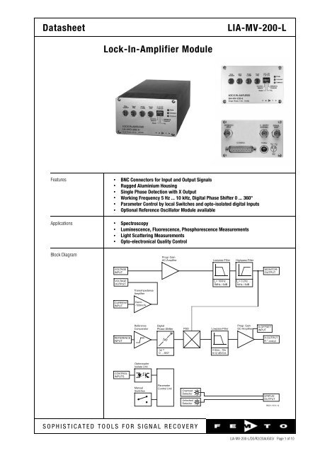
Datasheet LIA-MV-200-L Lock-In-Amplifier Module
Datasheet LIA-MV-200-L Lock-In-Amplifier Module
Datasheet LIA-MV-200-L Lock-In-Amplifier Module

Create successful ePaper yourself
Turn your PDF publications into a flip-book with our unique Google optimized e-Paper software.
<strong>Datasheet</strong><strong>LIA</strong>-<strong>MV</strong>-<strong>200</strong>-L<strong>Lock</strong>-<strong>In</strong>-<strong>Amplifier</strong> <strong>Module</strong>Specifications (continued)Output Output Channels X = <strong>In</strong> PhaseOutput Voltage Range ± 10 V (@ 2 kΩ Load)Output Current± 5 mA max.Output Impedance50 ΩOutput DC-Stability5 ppm/K @ Ultra Stable Setting50 ppm/K @ Low Drift Setting500 ppm/K @ High Dynamic SettingOutput Basic Accuracy 2 % @ sinusoidal input signalOutput Voltage Offset RangeOutput Voltage Offset Control-Output Load Impedance± 100 % Full Scale by ± 10 V Control Voltage> 2 kΩStatus <strong>In</strong>dicator LED Functions <strong>Amplifier</strong> Overload StatusReference PLL Unlocked StatusDigital Control Control <strong>In</strong>put Voltage Low: - 0.8 V ... + 0.8 V, High: + 1.8 V ... + 12 VControl <strong>In</strong>put Current0 mA @ 0V, 1.5 mA @ + 5 V, 4.5 mA @ + 12V typ.Digital Status Output Voltage Active: + 4.5 V typ., Non Active: 0 V typ.Digital Status Output Current 10 mA max.Power Supply Supply Voltage ± 15 Vdc ... ± 18 VdcSupply Current- 60 mA, + 100 mACase Material Aluminium anodizedDimension64,4 x 105,0 x 223,0 mm (without BNC-connectors)Weight1000 gr. (2.2 lbs)Temperature Range Storage Temperature - 40 ... + 100 °COperating Temperature 0 ... + 60 °CAbsolute Maximum Ratings Signal <strong>In</strong>put AC Voltage 50 VppReference <strong>In</strong>put Voltage ± 15 VControl <strong>In</strong>put Voltage- 5 V, + 30 VPower Supply Voltage ± 22 VSwitch Settings 4 Dip Switch - Presettings Switch OFF ON⎯⎯⎯⎯⎯⎯⎯⎯⎯⎯⎯⎯⎯⎯⎯⎯⎯⎯⎯⎯⎯S1 Low Drift & High Dynamic Ultra Stable & Low DriftS2 1-f Mode 2-f ModeS3 Fast PLL-<strong>Lock</strong>ing Slow PLL-<strong>Lock</strong>ingS4 Reference-<strong>In</strong>put- Reference-<strong>In</strong>put-Threshold = 0 V Threshold = +2 VSensitivity Setting,3 Output DC-Gain Modes are selectable:Output DC-Gain Modes Mode DC-Gain Dyn. Reserve DC-Stability⎯⎯⎯⎯⎯⎯⎯⎯⎯⎯⎯⎯⎯⎯⎯⎯⎯⎯⎯⎯⎯Ultra Stable 10 Low HighLow Drift 100 Medium MediumHigh Dynamic 1000 High LowIf only low dynamic reserve is required, select the higherDC-Stability settings. Use Dip switch S1 to preselect eitherthe two upper or the two lower DC-Gain modes, then selectbest mode by Sensitivity switch settings 0–7 or 8–F.SOPHISTICATED TOOLS FOR SIGNAL RECOVERYPage 3
<strong>Datasheet</strong><strong>LIA</strong>-<strong>MV</strong>-<strong>200</strong>-L<strong>Lock</strong>-<strong>In</strong>-<strong>Amplifier</strong> <strong>Module</strong>Switch Settings (continued) S1 = ON: Sensitivity Setting Ultra Stable Mode ⏐ Low Drift Modefor Full Scale ( = 10 V Output) Setting Voltage Current ⏐ Setting Voltage Current⎯⎯⎯⎯⎯⎯⎯⎯⎯⎯⎯⎯⎯⎯⎯⎯⎯⎯⎯⎯⎯0 1 V 10 µA ⏐ 8 100 mV 1 µA1 300 mV 3 µA ⏐ 9 30 mV 300 nA2 100 mV 1 µA ⏐ A 10 mV 100 nA3 30 mV 300 nA ⏐ B 3 mV 30 nA4 10 mV 100 nA ⏐ C 1 mV 10 nA5 3 mV 30 nA ⏐ D 300 µV 3 nA6 1 mV 10 nA ⏐ E 100 µV 1 nA7 300 µV 3 nA ⏐ F 30 µV 300 pAS1 = OFF: Sensitivity Setting Low Drift Mode ⏐ High Dynamic Modefor Full Scale ( = 10 V Output) Setting Voltage Current ⏐ Setting Voltage Current⎯⎯⎯⎯⎯⎯⎯⎯⎯⎯⎯⎯⎯⎯⎯⎯⎯⎯⎯⎯⎯0 100 mV 1 µA ⏐ 8 10 mV 100 nA1 30 mV 300 nA ⏐ 9 3 mV 30 nA2 10 mV 100 nA ⏐ A 1 mV 10 nA3 3 mV 30 nA ⏐ B 300 µV 3 nA4 1 mV 10 nA ⏐ C 100 µV 1 nA5 300 µV 3 nA ⏐ D 30 µV 300 pA6 100 µV 1 nA ⏐ E 10 µV 100 pA7 30 µV 300 pA ⏐ F 3 µV 30 pATime Constant Setting 6 dB/Oct. 12 dB/Oct. Time Constant⎯⎯⎯⎯⎯⎯⎯⎯⎯⎯⎯⎯⎯⎯0 8 3 ms1 9 10 ms2 A 30 ms3 B 100 ms4 C 300 ms5 D 1 s6 E 3 s7 F 10 sPhase Shift SettingPhase shift is adjusted by 2 phase switches with8 Bit resolution. Values 0 ... 255 ( Hex 00 ... FF )correspond to phase shift setting 0 ... +360 °.One step with switch marked “Coarse” changes phase shiftby 22.5 °. The “Fine”-switch changes phase shiftby 1.4 ° - steps:FineCoarse+180°+11,3°+135° 7 8 9 +225°6 A+8,4° 765+90° 4BC +270°5+5,6° 43D32 E2+45° 1 0 F +315° +2,8° 1 00°0°8 9 +14,1°ABC +16°DEF+19,7°If 2-f Mode is selected,the resolution of digital phase control changes to 2.8 °and the phase shift range doubles to 0 ... + 720 °.SOPHISTICATED TOOLS FOR SIGNAL RECOVERYPage 4
<strong>In</strong>terfaceControlConnectorExtensionOscillatorReferenceConnectorExtension<strong>Datasheet</strong><strong>LIA</strong>-<strong>MV</strong>-<strong>200</strong>-L<strong>Lock</strong>-<strong>In</strong>-<strong>Amplifier</strong> <strong>Module</strong><strong>In</strong>ternal Jumper Settings(jumpers are accessiblewhen top of case isremoved)<strong>In</strong>put Signal FilterSettingSet Cut-Off Frequency of <strong>In</strong>put Lowpass Filterwith JP1 + JP2 (always same position) andHighpass Filter with JP3:Highpass ⏐ LowpassJP3 -3 dB Cut-Off ⏐ JP1, JP2 -3 dB Cut-Off⎯⎯⎯⎯⎯⎯⎯⎯⎯⎯⎯⎯⎯⎯⎯⎯⎯⎯⎯⎯⎯3 – 4 0.2 Hz ⏐ 1 – 2 100 Hz1 – 3 1 Hz ⏐ 3 – 4 1 kHz2 – 4 10 Hz ⏐ 5 – 6 10 kHz3 – 5 100 Hz ⏐ 7 – 8 100 kHz4 – 6 1 kHz ⏐ none 1 MHzFrequency Range JP4 Frequency RangeSelection⎯⎯⎯⎯⎯⎯⎯⎯⎯⎯⎯⎯⎯⎯1 – 2 normal operation3, 4, 5, 6, 7, 8 test pins, do not use<strong>In</strong>ternal Jumper PositionDiagram(look at top of board whencase is opened)11753JP24628531JP17Monitor Output48629 7315JP324Filter Extension10 86X Freq. Comp.Connector1Amplitude AdjustFrequency AdjustY Freq. Comp.213456X Offset AdjustJP678X Gain AdjustOptional ReferenceOscillator <strong>Module</strong>8642Trimmer for ServiceJP4purposes only !7531Y Offset AdjustY Gain Adjust<strong>Lock</strong>-<strong>In</strong>-<strong>Amplifier</strong> BoardSOPHISTICATED TOOLS FOR SIGNAL RECOVERYPage 5
<strong>Datasheet</strong><strong>LIA</strong>-<strong>MV</strong>-<strong>200</strong>-L<strong>Lock</strong>-<strong>In</strong>-<strong>Amplifier</strong> <strong>Module</strong><strong>In</strong>ternal Connector(of build-in <strong>Lock</strong>-<strong>In</strong> Board)Connector TypeEuro-Card DIN 41612 Connector, 64 pin male, (a+c)<strong>In</strong>put Pin C2: Voltage <strong>In</strong>put, Non <strong>In</strong>verting, DC-CoupledPin C3: Voltage <strong>In</strong>put, Non <strong>In</strong>verting, AC-CoupledPin C4: Voltage <strong>In</strong>put, <strong>In</strong>verting, AC-CoupledPin C5: Voltage <strong>In</strong>put, <strong>In</strong>verting, DC-CoupledPin C7: Current <strong>In</strong>putPin C6: Current <strong>Amplifier</strong> Voltage OutputPin A2- A6: <strong>In</strong>put GNDMonitor Output Pin C9: Monitor OutputPin A9: Monitor GNDOutput Pin C14: X-Signal OutputPin C15: Output GNDOffset <strong>In</strong>put Pin A10: X-Offset <strong>In</strong>putPin A13: Offset GNDStatus Output Pin C10: Unlocked Status OutputPin C11: Overload Status OutputPin C17: Status Output GND (=Power Supply GND)Power Supply Pin A16+C16: Power Supply – 15VPin A18+C18: Power Supply + 15VPin A17+C17: Power Supply GNDRemote Control <strong>In</strong>puts Pin C19: Time Constant (TC0)(Opto-Isolated) Pin A19: Time Constant (TC1)Pin C20: Time Constant (TC2)Pin A20: Time Constant Slope (TCSL)Pin A22: Sensitivity (SEN0)Pin C21: Sensitivity (SEN1)Pin A21: Sensitivity (SEN2)Pin C22: Dynamic Mode (DYN0)Pin A28: Phase Shift (PH0)Pin C28: Phase Shift (PH1)Pin A27: Phase Shift (PH2)Pin C27: Phase Shift (PH3)Pin A26: Phase Shift (PH4)Pin C26: Phase Shift (PH5)Pin A25: Phase Shift (PH6)Pin C25: Phase Shift (PH7)Pin C24: Disable Local Switch ControlPin A23+A24: Remote Control GND(Common Optocoupler Cathode)Reference <strong>In</strong>put Pin A32: Reference <strong>In</strong>putPin A31: Reference <strong>In</strong>put GroundReference Output Pin A30: Reference Output(Connected only if optional Pin A17: Refer. Output GND (=Power Supply GND)Oscillator <strong>Module</strong> is installed) Pin A29: Reference Synchronization <strong>In</strong>putStandard Control <strong>In</strong>terface Pin C29: <strong>In</strong>terface 0(Connected only if optional Pin C30: <strong>In</strong>terface 1Control <strong>In</strong>terface <strong>Module</strong> Pin C31: <strong>In</strong>terface 2(future product) is installed) Pin C32: <strong>In</strong>terface 3SOPHISTICATED TOOLS FOR SIGNAL RECOVERYPage 6
2 PIN-15V<strong>Datasheet</strong><strong>LIA</strong>-<strong>MV</strong>-<strong>200</strong>-L<strong>Lock</strong>-<strong>In</strong>-<strong>Amplifier</strong> <strong>Module</strong>External Connectors(at backside, StandardConfiguration)Signal <strong>In</strong>putX-OutputFactory set to BNC, isolated (single ended)BNCReference <strong>In</strong>putPower SupplyBNCLEMO Series 1S, 3-pin fixed SocketPin 1: + 15VPin 2: - 15VPin 3: GNDPIN 1+15VPIN 3GNDControl Port Sub-D 25-pin, female, Qual. Class 2Pin 1: +12V (Stabilized Power Supply Output)Pin 2: -12V (Stabilized Power Supply Output)Pin 3: AGND (Analog Ground)Pin 4: +5V (Stabilized Power Supply Output)Pin 5: X-OutputPin 6: Overload Status OutputPin 7: Unlocked Status OutputPin 8: Disable Local Switch Control <strong>In</strong>putPin 9: DGND (Ground f. Digital Control Pin 8 - 25)Pin 10: Dynamic Mode (DYN0)Pin 11: Sensitivity (SEN0)Pin 12: Sensitivity (SEN1)Pin 13: Sensitivity (SEN2)Pin 14: Time Constant Slope (TCSL)Pin 15: Time Constant (TC0)Pin 16: Time Constant (TC1)Pin 17: Time Constant (TC2)Pin 18: Phase Shift (PH0)Pin 19: Phase Shift (PH1)Pin 20: Phase Shift (PH2)Pin 21: Phase Shift (PH3)Pin 22: Phase Shift (PH4)Pin 23: Phase Shift (PH5)Pin 24: Phase Shift (PH6)Pin 25: Phase Shift (PH7)Connector Wiring Options General The BNC-connector configuration can be easily changed bysetting electrical jumpers at the internal I/O-adapter card.Disconnect the power supply and open the case byloosening the two upper screws at the case front and rearside. Please pay attention to the ground connection at thebackplane. Now open the case by lifting the top.The jumper options and functions are described in thefollowing table.SOPHISTICATED TOOLS FOR SIGNAL RECOVERYPage 7
<strong>Datasheet</strong><strong>LIA</strong>-<strong>MV</strong>-<strong>200</strong>-L<strong>Lock</strong>-<strong>In</strong>-<strong>Amplifier</strong> <strong>Module</strong>Connector Wiring Options,Jumpers on internalAdapter Board<strong>In</strong>put Connectors (JP1) <strong>In</strong>put wiring Jumper installed⎯⎯⎯⎯⎯⎯⎯⎯⎯⎯⎯⎯⎯⎯⎯⎯⎯⎯⎯⎯⎯IN A = Voltage <strong>In</strong>put "+V-IN → IN A"(Single Ended, AC) "GND → IN A/SHLD""-V-IN → IN A/SHLD"IN A = Voltage <strong>In</strong>put "+V-IN → IN A"(Differential, AC)"-V-IN → IN A/SHLD"IN A / IN B = Voltage <strong>In</strong>put "+V-IN → IN A"(2 BNC Differential, AC) "GND → IN A/SHLD"(OUT A cannot be used) "-V-IN → IN B"IN A = Current <strong>In</strong>put "C-IN → IN A"(Single Ended)"GND → IN A/SHLD""-V-IN → C-OUT"Output Connectors (JP2) Output wiring Jumper installed⎯⎯⎯⎯⎯⎯⎯⎯⎯⎯⎯⎯⎯⎯⎯⎯⎯⎯⎯⎯⎯OUT A = X-Output "X → OUT A"(JP1) "USE OUT A/NO IN B"OUT B = X-Output "X → OUT B"OUT A = Y-Output "Y → OUT A"(JP1) "USE OUT A/NO IN B"OUT B = Y-Output "Y → OUT B"OUT C = Y-Output "Y → OUT C"OUT A = R-Output "R → OUT A"(JP1) "USE OUT A/NO IN B"OUT B = R-Output "R → OUT B"OUT C = R-Output "R → OUT C"OUT B = Monitor Output "MON → OUT B"OUT C = Monitor Output "MON → OUT C"OUT B = Unlocked Output "UNL → OUT B"OUT C = Unlocked Output "UNL → OUT C"OUT B = Overload Output "OVL → OUT B"OUT C = Overload Output "OVL → OUT C"OUT C = Reference Output "REF-OUT → OUT C"Reference Connector (JP3) Reference wiring Jumper installed⎯⎯⎯⎯⎯⎯⎯⎯⎯⎯⎯⎯⎯⎯⎯⎯⎯⎯⎯⎯⎯REF = Reference <strong>In</strong>put "REF-IN → REF" (2 Jumper)(Reference Output only if REF = Reference Output "REF-OUT → REF-IN" (2 Jp.)optional Oscillator <strong>Module</strong> (Reference Output "REF-IN → REF" (2 Jumper)is installed)connected to Ref. <strong>In</strong>put)REF = Refer. Sync. <strong>In</strong>put "REF-SYNC → REF" (2 Jp.)(use OUT C asReference Output)SOPHISTICATED TOOLS FOR SIGNAL RECOVERYPage 8
<strong>Datasheet</strong><strong>LIA</strong>-<strong>MV</strong>-<strong>200</strong>-L<strong>Lock</strong>-<strong>In</strong>-<strong>Amplifier</strong> <strong>Module</strong>Remote Control Operation General Remote Control <strong>In</strong>put Bits are opto-isolated and connectedby logical OR to local switch setting. The 4 hexadecimalswitches are 4 Bit-coded as shown in the following table:MSBLSBSwitch Code Bit 3 Bit 2 Bit 1 Bit 0⎯⎯⎯⎯⎯⎯⎯⎯⎯⎯⎯⎯⎯⎯⎯⎯0 Low Low Low Low1 Low Low Low High2 Low Low High Low3 Low Low High High4 Low High Low Low5 Low High Low High6 Low High High Low7 Low High High High8 High Low Low Low9 High Low Low HighA High Low High LowB High Low High HighC High High Low LowD High High Low HighE High High High LowF High High High HighFor remote control a switch setting, set the local switchto “0” and select the wanted setting via the 4-Bit-codeat the corresponding digital inputs.Sensitivity Switch - Bit Corresponding Control Port <strong>In</strong>putCorresponding <strong>In</strong>puts ⎯⎯⎯⎯⎯⎯⎯⎯⎯⎯⎯⎯⎯⎯⎯Bit 0 SEN0 (Pin A22)Bit 1 SEN1 (Pin C21)Bit 2 SEN2 (Pin A21)Bit 3 DYN0 (Pin C22)Time Constant Switch - Bit Corresponding Control Port <strong>In</strong>putCorresponding <strong>In</strong>puts ⎯⎯⎯⎯⎯⎯⎯⎯⎯⎯⎯⎯⎯⎯⎯Bit 0 TC0 (Pin C19)Bit 1 TC1 (Pin A19)Bit 2 TC2 (Pin C20)Bit 3 TCSL (Pin A20)Phase Switch Coarse - Bit Corresponding Control Port <strong>In</strong>putCorresponding <strong>In</strong>puts ⎯⎯⎯⎯⎯⎯⎯⎯⎯⎯⎯⎯⎯⎯⎯Bit 0 PH4 (Pin A26)Bit 1 PH5 (Pin C26)Bit 2 PH6 (Pin A25)Bit 3 PH7 (Pin C25)Phase Switch Fine - Bit Corresponding Control Port <strong>In</strong>putCorresponding <strong>In</strong>puts ⎯⎯⎯⎯⎯⎯⎯⎯⎯⎯⎯⎯⎯⎯⎯Bit 0 PH0 (Pin A28)Bit 1 PH1 (Pin C28)Bit 2 PH2 (Pin A27)Bit 3 PH3 (Pin C27)Remote Control ExampleFor example, to select a switch setting code “6”, you haveto connect a “High”- level signal to the correspondingcontrol input pins Bit 1 & Bit 2. Mixed operation, e.g. localphase settings and remote controlled sensitivity setting, isalso possible.SOPHISTICATED TOOLS FOR SIGNAL RECOVERYPage 9
Time-ConstantREFERENCEINPUTSensitivityPhaseCoarseLOCK-IN-AMPLIFIER<strong>LIA</strong>-<strong>MV</strong>-<strong>200</strong>-LPhaseFineDynamicReserveH F 1f 0V2f 2V S L- OUTPUT X(IN-PHASE)ReferenceThresholdSIGNALINPUT<strong>Datasheet</strong><strong>LIA</strong>-<strong>MV</strong>-<strong>200</strong>-L<strong>Lock</strong>-<strong>In</strong>-<strong>Amplifier</strong> <strong>Module</strong>DimensionsTop ViewFront ViewPower64,4 mmUnlockedOverloadPLLModeSingle Phase, 5 Hz - 10 kHz105,0 mm223,0 mmBack ViewPOWERPIN 1PIN 2CONTROL-15V+15VPIN 3GNDCase Material:Al, natural anodisedDZ01-1071-10Optional Extensions Reference Oscillator <strong>Module</strong> Model No.: SOM-1- Frequency Range 5 Hz ... 130 kHz, User adjustable- Output Voltage 0 ... 2 Vrms, User adjustable- 100 ppm/K Amplitude AccuracyFactory Set1 kHz, 1 VrmsFEMTO Messtechnik GmbHPaul Lincke-Ufer 34D-10999 Berlin GermanyTel.: +49 (0)30 – 4 46 93 86Fax: +49 (0)30 – 4 46 93 88e-mail: info@femto.dehttp://www.femto.deSpecifications are subject to change without notice. <strong>In</strong>formation furnished herin is believed tobe accurate and reliable. However, no responsibility is assumed by FEMTO MesstechnikGmbH for its use, nor for any infringement of patents or other rights granted by implicationor otherwise under any patent rights of FEMTO Messtechnik GmbH. Product namesmentioned may also be trademarks used here for identification purposes only.© by FEMTO Messtechnik GmbHPrinted in GermanySOPHISTICATED TOOLS FOR SIGNAL RECOVERYPage 10