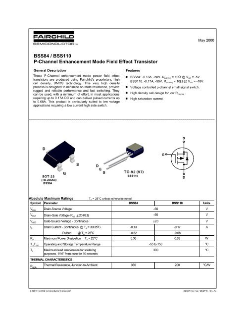
BSS84/BSS110 P-Channel Enhancement Mode Field Effect Transistor
BSS84/BSS110 P-Channel Enhancement Mode Field Effect Transistor
BSS84/BSS110 P-Channel Enhancement Mode Field Effect Transistor
- No tags were found...

You also want an ePaper? Increase the reach of your titles
YUMPU automatically turns print PDFs into web optimized ePapers that Google loves.
ELECTRICAL CHARACTERISTICS (T A= 25°C unless otherwise noted)Symbol Parameter Conditions Type Min Typ Max UnitsOFF CHARACTERISTICSBV DSSDrain-Source Breakdown Voltage V GS= 0 V, I D= -250 µA All -50 VI DSSZero Gate Voltage Drain Current V DS= -50 V,V GS= 0 VAll -15 µAT J= 125°C -60 µAV DS= -25 V, V GS= 0 V -0.1 µAI GSSRGate - Body Leakage, Reverse V GS= -20 V, V DS= 0 V All -10 nAON CHARACTERISTICS (Note 1)V GS(th)Gate Threshold Voltage V DS= V GS, I D= -1 mA All -0.8 -1.75 -2 VR DS(ON)Static Drain-Source On-Resistance V GS= -5V, I D= -0.10 A <strong>BSS84</strong> 3.2 10 ΩV GS= -10 V, I D= -0.17 A <strong>BSS110</strong> 2.2 10g FSForward Transconductance V DS= -25 V, I D= -0.10A <strong>BSS84</strong> 0.05 0.27 SDYNAMIC CHARACTERISTICSC issInput Capacitance V DS= -25 V, V GS= 0 V,f = 1.0 MHzV DS= -10 V, I D= -0.17 A <strong>BSS110</strong> 0.05 0.29<strong>BSS84</strong> 37 45 pF<strong>BSS110</strong> 37 40C ossOutput Capacitance All 16 25 pFC rssReverse Transfer Capacitance All 5 12 pFSWITCHING CHARACTERISTICS (Note 1)t D(on)Turn - On Delay Time V DD= -30 V, I D= -0.27 A,All 12 nSt rTurn - On Rise Time V GS= -10 V, R GEN= 50 ΩAll 50 nSt D(off)Turn - Off Delay Time All 10 nSt fTurn - Off Fall Time All 25 nSDRAIN-SOURCE DIODE CHARACTERISTICSI SContinuous Source Diode Current <strong>BSS84</strong> -0.13 A<strong>BSS110</strong> -0.17I SMMaximum Pulsed Source Diode Current (Note 1) <strong>BSS84</strong> -0.52 A<strong>BSS110</strong> -0.68V SDDrain-Source Diode Forward Voltage V GS= 0 V, I S= -0.26 A (Note 1) <strong>BSS84</strong> -0.95 -1.2 VNote:1. Pulse Test: Pulse Width < 300 µs, Duty Cycle < 2.0%.V GS= 0 V, I S= -0.34 A (Note 1) <strong>BSS110</strong> -1 -1.2<strong>BSS84</strong> Rev. C2 / <strong>BSS110</strong>. Rev. A3
DTypical Electrical CharacteristicsI , DRAIN-SOURCE CURRENT (A)D-1-0.8-0.6-0.4-0.2V = -10VGS-8.0-6.0-5.0-4.5-4.0-3.5-3.0-2.5R DS(on) , NORMALIZEDDRAIN-SOURCE ON-RESISTANCE32.521.51V = -3VGS-3.5-4.0-4.5-5.0-6.0-8.0-100-1-2 -3 -4V DS , DRAIN-SOURCE VOLTAGE (V)-5-60.5-0.2-0.4 -0.6I , DRAIN CURRENT (A)D-0.8-1Figure 1. On-Region CharacteristicsFigure 2. On-Resistance Variationwith Drain Current and Gate Voltage1.63R DS(ON) , NORMALIZEDDRAIN-SOURCE ON-RESISTANCE1.41.210.8I D = -0.13AV = -10VGSR DS(on) , NORMALIZEDDRAIN-SOURCE ON-RESISTANCE2.521.51V = -10VGST = 125°CJ25°C-55°C0.6-50 -25 0 25 50 75 100 125 150T J , JUNCTION TEMPERATURE (°C)0.5-0.2-0.4 -0.6I D , DRAIN CURRENT (A)-0.8-1Figure 3. On-Resistance Variationwith TemperatureFigure 4. On-Resistance Variationwith Drain Current and TemperatureI , DRAIN CURRENT (A)-1-0.8-0.6-0.4-0.2V = -10VDST = -55°C J25°C 125°CV , NORMALIZEDthGATE-SOURCE THRESHOLD VOLTAGE1.11.0510.950.9V DS = V GSI D = -1mA0-2-4-6VGS, GATE TO SOURCE VOLTAGE (V)-80.85-50 -25 0 25 50 75 100 125 150T , JUNCTION TEMPERATURE (°C)JFigure 5. Transfer CharacteristicsFigure 6. Gate Threshold Variationwith Temperature<strong>BSS84</strong> Rev. C2 / <strong>BSS110</strong>. Rev. A3
STypical Electrical Characteristics (continued)BV , NORMALIZEDDSSDRAIN-SOURCE BREAKDOWN VOLTAGE1.11.0510.95I D = -250µA0.9-50 -25 0 25 50 75 100 125 150TJ, JUNCTION TEMPERATURE (°C)-I , REVERSE DRAIN CURRENT (A)10.50.20.10.050.010.005V GS = 0VT = 125°C J25°C-55°C0.0010.2 0.4 0.6 0.8 1 1.2 1.4 1.6-V SD , BODY DIODE FORWARD VOLTAGE (V)Figure 7. Breakdown VoltageVariation with TemperatureFigure 8. Body Diode Forward VoltageVariation with SourceCurrent and Temperature7010CAPACITANCE (pF)5030201053f = 1 MHzV GS = 0VC issC ossC rss-V GS , GATE-SOURCE VOLTAGE (V)8642I D= -0.13AV = -10VDS-20V-40V20.1 0.2 0.5 1 2 5 10 20 30 50-VDS, DRAIN TO SOURCE VOLTAGE (V)Figure 9. Capacitance Characteristics00 0.5 1 1.5 2Q g , GATE CHARGE (nC)Figure 10. Gate Charge CharacteristicsV GSV DDR Lon offt d(on) t tr d(off)VIN90%90%DV OUTV OUT10%10%R GENGDUT90%tttfFigure 11. Switching Test CircuitSV IN 50%50%10%PULSE WIDTHFigure 12. Switching WaveformsINVERTED<strong>BSS84</strong> Rev. C2 / <strong>BSS110</strong>. Rev. A3
Typical Electrical Characteristics (continued)g , TRANSCONDUCTANCE (SIEMENS)FS0.50.40.30.20.10-0.2T = -55°C J25°C-0.4 -0.6I , DRAIN CURRENT (A)D125°CV = -10VDSFigure 13. Transconductance Variation with DrainCurrent and Temperature-0.8-1-I , DRAIN CURRENT (A)D210.50.10.050.01RDS(ON) LimitV GS = -10VSINGLE PULSET A = 25°C100ms1s10sDC1ms10ms100us0.0051 2 5 10 20 30 50 80- V DS , DRAIN-SOURCE VOLTAGE (V)Figure 14. Maximum Safe Operating Arear(t), NORMALIZED EFFECTIVETRANSIENT THERMAL RESISTANCE10.50.20.10.050.010.002D = 0.50.20.10.050.020.01Single PulseRθJA(t) = r(t) * RθJAR = 350 C/WθJAT J - TA= P * R θJA(t)Duty Cycle, D = t 1 /t20.0010.0001 0.001 0.01 0.1 1 10 100 300t 1, TIME (sec)Figure 15. Transient Thermal Response CurveNote : Characterization performed using a circuit board with 175 o C/Wtypical case-to-ambient thermal resistance.P(pk)t 1t 2o<strong>BSS84</strong> Rev. C2 / <strong>BSS110</strong>. Rev. A3
TO-92 Package DimensionsTO-92; TO-18 Reverse Lead Form (J35Z Option)(FS PKG Code 92, 94, 96)1:1Scale 1:1 on letter size paperDimensions shown below are in:inches [millimeters]Part Weight per unit (gram): 0.22* * ;Note: All package 97 or 98 transistors are leadformedto this configuration prior to bulk shipment. OrderL34Z option if in-line leads are preferred on package97 or 98.* Standard Option on 97 & 98 package codeJanuary 2000, Rev. B
TRADEMARKSThe following are registered and unregistered trademarks Fairchild Semiconductor owns or is authorized to use and isnot intended to be an exhaustive list of all such trademarks.ACExBottomlessCoolFETCROSSVOLTDenseTrenchDOMEEcoSPARKE 2 CMOS TMEnSigna TMFACTFACT Quiet SeriesSTAR*POWER is used under licenseDISCLAIMERFAIRCHILD SEMICONDUCTOR RESERVES THE RIGHT TO MAKE CHANGES WITHOUT FURTHERNOTICE TO ANY PRODUCTS HEREIN TO IMPROVE RELIABILITY, FUNCTION OR DESIGN. FAIRCHILDDOES NOT ASSUME ANY LIABILITY ARISING OUT OF THE APPLICATION OR USE OF ANY PRODUCTOR CIRCUIT DESCRIBED HEREIN; NEITHER DOES IT CONVEY ANY LICENSE UNDER ITS PATENTRIGHTS, NOR THE RIGHTS OF OTHERS.LIFE SUPPORT POLICYFAIRCHILD’S PRODUCTS ARE NOT AUTHORIZED FOR USE AS CRITICAL COMPONENTS IN LIFE SUPPORTDEVICES OR SYSTEMS WITHOUT THE EXPRESS WRITTEN APPROVAL OF FAIRCHILD SEMICONDUCTOR CORPORATION.As used herein:1. Life support devices or systems are devices orsystems which, (a) are intended for surgical implant intothe body, or (b) support or sustain life, or (c) whosefailure to perform when properly used in accordancewith instructions for use provided in the labeling, can bereasonably expected to result in significant injury to theuser.PRODUCT STATUS DEFINITIONSDefinition of TermsFAST ®FASTrFRFETGlobalOptoisolatorGTOHiSeCISOPLANARLittleFETMicroFETMICROWIREOPTOLOGICOPTOPLANARPACMANPOPPower247PowerTrench®QFETQSQT OptoelectronicsQuiet Series®SILENT SWITCHERSMART START2. A critical component is any component of a lifesupport device or system whose failure to perform canbe reasonably expected to cause the failure of the lifesupport device or system, or to affect its safety oreffectiveness.Datasheet Identification Product Status DefinitionSTAR*POWERStealthSuperSOT-3SuperSOT-6SuperSOT-8SyncFETTinyLogicTruTranslationUHC®UltraFETVCXAdvance InformationPreliminaryNo Identification NeededFormative orIn DesignFirst ProductionFull ProductionThis datasheet contains the design specifications forproduct development. Specifications may change inany manner without notice.This datasheet contains preliminary data, andsupplementary data will be published at a later date.Fairchild Semiconductor reserves the right to makechanges at any time without notice in order to improvedesign.This datasheet contains final specifications. FairchildSemiconductor reserves the right to make changes atany time without notice in order to improve design.ObsoleteNot In ProductionThis datasheet contains specifications on a productthat has been discontinued by Fairchild semiconductor.The datasheet is printed for reference information only.Rev. H3