FDR6580 N-Channel 2.5V Specified PowerTrench MOSFET - DigiKey
FDR6580 N-Channel 2.5V Specified PowerTrench MOSFET - DigiKey
FDR6580 N-Channel 2.5V Specified PowerTrench MOSFET - DigiKey

Create successful ePaper yourself
Turn your PDF publications into a flip-book with our unique Google optimized e-Paper software.
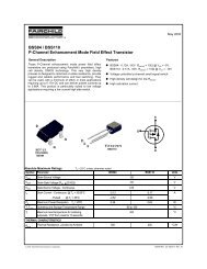
<strong>FDR6580</strong>N-Chennal <strong>2.5V</strong> <strong>Specified</strong> <strong>PowerTrench</strong> TM <strong>MOSFET</strong>April 1999ADVANCE INFORMATION<strong>FDR6580</strong>General DescriptionThis N-<strong>Channel</strong> <strong>2.5V</strong> specified <strong>MOSFET</strong> is produced usingFairchild Semiconductor's advanced <strong>PowerTrench</strong> processthat has been especially tailored to minimize the on-stateresistance and yet maintain low gate charge for superiorswitching performance.Applications• Load switch• Motor driving• Power ManagementFeatures• 11 A, 20 V. R DS(ON)= 0.009 Ω @ V GS= 4.5 VR DS(ON)= 0.013 Ω @ V GS= 2.5 V.• Low gate charge.• High performance trench technology for extremelylow R DS(ON).• Small footprint (38% smaller than a standard SO-8); lowprofile package (1 mm thick); power handling capabilitysimilar to SO-8.SDDS5643TMSuperSOT -8DDDG7821Absolute Maximum Ratings T A = 25°C unless otherwise notedSymbol Parameter Ratings UnitsV DSS Drain-Source Voltage 20 VV GSS Gate-Source Voltage ±8 VI D Drain Current - Continuous (Note 1a) 11 A- Pulsed 50P D Power Dissipation for Single Operation (Note 1a) 1.8 W(Note 1b) 1.0(Note 1c) 0.9T J , T stg Operating and Storage Junction Temperature Range -55 to +150 °CThermal CharacteristicsR θ JA Thermal Resistance, Junction-to-Ambient (Note 1a) 70 °C/WR θ JC Thermal Resistance, Junction-to-Case (Note 1) 20 °C/WPackage Outlines and Ordering InformationDevice Marking Device Reel Size Tape Width Quantity.6580 <strong>FDR6580</strong> 13’’ 12mm 3000 units©1999 Fairchild Semiconductor Corporation<strong>FDR6580</strong>, Rev. A
Electrical CharacteristicsTA=25 o C unless otherwise notedSymbol Parameter Test Conditions Min Typ Max Units<strong>FDR6580</strong>OFF CHARACTERISTICSBV DSS Drain-Source Breakdown Voltage V GS = 0 V, I D = 250 µA 20 VI DSS Zero Gate Voltage Drain Current V DS = 16 V, V GS = 0 V 1 µAI GSSF Gate-Body Leakage, Forward V GS = 8 V, V DS = 0 V 10 µAI GSSR Gate-Body Leakage, Reverse V GS = -8 V, V DS = 0 V -10 µAON CHARACTERISTICS (Note 2)V GS(TH) Gate Threshold Voltage V DS = V GS, I D = 250 µA 0.4 1.5 VR DS(ON)Static Drain-SourceOn-ResistanceV GS = 4.5 V, I D = 11 AV GS = 2.5 V, I D = 9.3 A0.0090.013I D(ON) On-State Drain Current V GS = 4.5 V, V DS = 5 V 25 AΩDRAIN-SOURCE DIODE CHARACTERISTICS AND MAXIMUM RATINGSI S Maximum Continuous Drain-Source Diode Forward Current 1.5 AV SDDrain-Source Diode ForwardVoltageNotes:1. R θJAis the sum of the junction-to-case and case-to-ambient resistance where the case thermal reference is defined as the solder mounting surface ofthe drain pins. R θJCis guaranteed by design while R θCAis determined by the user's board design.V GS = 0 V, I S = 1.5 A (Note 2) 1.2 Va) 70° C/W when mounted on a1.0 in 2 pad of 2 oz. copper.b) 125° C/W when mounted ona 0.026 in 2 pad of 2oz. copper.c) 135° C/W when mountedon a minimum pad.Scale 1 : 1 on letter size paper2. Pulse Test: Pulse Width ≤ 300 µs, Duty Cycle ≤ 2.0%<strong>FDR6580</strong>, Rev. A
SuperSOT TM -8 Tape and Reel Data and Package DimensionsSSOT-8 PackagingConfiguration: Figure 1.0Customized LabelF63TNR LabelAntistatic Cover TapeStatic Dissi pativeEmboss ed Carrier TapePackaging Description:SSOT-8 parts are shipped in tape. The carrier tape ismade from a di ssipat ive (carbo n filled) po ly carbon ateresin. The cover tape is a multilayer film (Heat ActivatedAdhesive in nature) primarily composed of polyester film ,adhesive layer, sealant, and anti-static sprayed agent.These reeled parts in standard option are shipped w ith3,000 units per 13" or 330cm diameter reel. The reels aredark blue in color and is made of polystyrene plastic (antistaticcoated). Other option comes in 500 units per 7" or177cm diameter reel. This and some other options arefurther described in the Packaging Information table.These full reels are in di vidu ally barcod e labeled andplaced inside a standard intermediate box (illustrated infigure 1.0) made of recyclable corrugated brown paper.One box contains two reels maximum. And these boxesare placed ins ide a barcode labeled shipping box whic hcomes in di fferent sizes depend in g on t he nu mber of partsshippe d.F852831NF852831NF852831NF852831NF852831NPin 1Packaging OptionPackaging typeReel SizeSSOT-8 Packaging InformationNote/CommentsStandard(no flow c ode )TNR13" D iaD84ZTNRQty per Reel/Tube/Bag 3,000 5007" DiaBox Dimension (mm) 343x64x343 184x187x47Max qty per Box 6,000 1,000Weight per unit (gm) 0.0416 0.0416Weight per Reel (kg) 0.5615 0.0980SSOT-8 Unit Orientation343mm x 342mm x 64mmIntermediate box for Standardand L99Z OptionsF63TNR LabelF63TNRLabel184mm x 187mm x 47mmPizza Box fo r D84Z OptionF63TNRLabelSSOT-8 Tape Leader and TrailerConfiguration: Figur e 2.0F63TNR Label sampl eLOT: CBVK741B019QTY: 3000FSID: FDR835NSPEC:D/C1: D9842 QTY1: SPEC REV:D/C2: QTY2: CPN:N/F: F (F63TNR)3Carrier TapeCover TapeTrailer Tape300mm mi nimum or38 empty pocketsComponentsLead er Tape500mm mi nimum or62 empty poc ketsAugust 1999, Rev. C
SuperSOT TM -8 Tape and Reel Data and Package Dimensions, continuedSSOT-8 Embossed Carrier TapeConfiguration: Figur e 3.0TP0D0E1FK0WcB0E2WTcA0P1D1User Direction of FeedDimensions are in millimeterPkg type A0 B0 W D0 D1 E1 E2 F P1 P0 K0 T Wc TcSSOT-8(12mm)4.47+/-0.105.00+/-0.1012.0+/-0.31.55+/-0.051.50+/-0.101.75+/-0.1010.25mi n5.50+/-0.058.0+/-0.14.0+/-0.11.37+/-0.100.280+/-0.1509.5+/-0.0250.06+/-0.02Notes : A0, B0, and K0 dimensions are determined with r espec t to t he EIA/Jedec RS-481rotationa l and lateral movement requi remen ts (see sketches A, B, and C).20 deg maximum0.5mmmaximumB0Typicalcomponentcavitycenter line0.5mmmaximum20 deg maximum component rotationSketch A (Si de or Front Sectional View)Component RotationSSOT-8 Reel Configuration: Figur e 4.0A0Sketch B (Top View)Component RotationTypicalcomponentcenter lineSketch C (Top View)Component lateral movementW1 Measured at HubDim AMaxDim AmaxDim N7" Diameter OptionSee detail AAB MinDim CSee detail AAW3Dim Dmin13" Diameter OptionW2 max Measured at HubDETAIL AATape SizeReelOptionDimensions are in inches and millimetersDim A Dim B Dim C Dim D Dim N Dim W1 Dim W2 Dim W3 (LSL-USL)12mm7" Dia7.00177.80.0591.5512 +0.020/-0.00813 +0.5/-0.20.79520.25.9061500.488 +0.078/-0.00012.4 +2/00.72418.40.469 – 0.60611.9 – 15.412mm13" Dia13.003300.0591.5512 +0.020/-0.00813 +0.5/-0.20.79520.27.001780.488 +0.078/-0.00012.4 +2/00.72418.40.469 – 0.60611.9 – 15.4© 1998 Fairchild Semiconductor CorporationJuly 1999, Rev. C
SuperSOT TM -8 Tape and Reel Data and Package Dimensions, continuedSuperSOT-8 (FS PKG Code 34, 35)1 : 1Scale 1:1 on letter size paperDimensions shown below are in:inches [millimeters]Part Weight per unit (gram): 0.0416September 1998, Rev. A
TRADEMARKSThe following are registered and unregistered trademarks Fairchild Semiconductor owns or is authorized to use and isnot intended to be an exhaustive list of all such trademarks.DISCLAIMERACExCoolFETCROSSVOLTE 2 CMOS TMFACTFACT Quiet SeriesFAST ®FASTrGTOHiSeCISOPLANARMICROWIREPOP<strong>PowerTrench</strong>®QFETQSQuiet SeriesSuperSOT-3SuperSOT-6SuperSOT-8TinyLogicUHCVCXFAIRCHILD SEMICONDUCTOR RESERVES THE RIGHT TO MAKE CHANGES WITHOUT FURTHERNOTICE TO ANY PRODUCTS HEREIN TO IMPROVE RELIABILITY, FUNCTION OR DESIGN. FAIRCHILDDOES NOT ASSUME ANY LIABILITY ARISING OUT OF THE APPLICATION OR USE OF ANY PRODUCTOR CIRCUIT DESCRIBED HEREIN; NEITHER DOES IT CONVEY ANY LICENSE UNDER ITS PATENTRIGHTS, NOR THE RIGHTS OF OTHERS.LIFE SUPPORT POLICYFAIRCHILD’S PRODUCTS ARE NOT AUTHORIZED FOR USE AS CRITICAL COMPONENTS IN LIFE SUPPORTDEVICES OR SYSTEMS WITHOUT THE EXPRESS WRITTEN APPROVAL OF FAIRCHILD SEMICONDUCTOR CORPORATION.As used herein:1. Life support devices or systems are devices orsystems which, (a) are intended for surgical implant intothe body, or (b) support or sustain life, or (c) whosefailure to perform when properly used in accordancewith instructions for use provided in the labeling, can bereasonably expected to result in significant injury to theuser.PRODUCT STATUS DEFINITIONSDefinition of Terms2. A critical component is any component of a lifesupport device or system whose failure to perform canbe reasonably expected to cause the failure of the lifesupport device or system, or to affect its safety oreffectiveness.Datasheet Identification Product Status DefinitionAdvance InformationPreliminaryNo Identification NeededFormative orIn DesignFirst ProductionFull ProductionThis datasheet contains the design specifications forproduct development. Specifications may change inany manner without notice.This datasheet contains preliminary data, andsupplementary data will be published at a later date.Fairchild Semiconductor reserves the right to makechanges at any time without notice in order to improvedesign.This datasheet contains final specifications. FairchildSemiconductor reserves the right to make changes atany time without notice in order to improve design.ObsoleteNot In ProductionThis datasheet contains specifications on a productthat has been discontinued by Fairchild semiconductor.The datasheet is printed for reference information only.