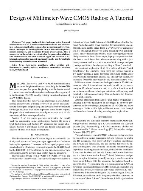
Design of Millimeter-Wave CMOS Radios: A Tutorial - UCLA ...
Design of Millimeter-Wave CMOS Radios: A Tutorial - UCLA ...
Design of Millimeter-Wave CMOS Radios: A Tutorial - UCLA ...
You also want an ePaper? Increase the reach of your titles
YUMPU automatically turns print PDFs into web optimized ePapers that Google loves.
6 IEEE TRANSACTIONS ON CIRCUITS AND SYSTEMS—I: REGULAR PAPERS, VOL. 56, NO. 1, JANUARY 20093) In deep-submicron technologies, most transistors are surroundedby dummy gate fingers so as to reduce mismatchesresulting from the stress due to shallow trench isolation[39], [40]. The position and number <strong>of</strong> these fingers dependon the particular circuit design and layout but theyaffect the extrinsic connections to the device and hence itsmodel.4) Reliance on measurement-based models prohibits the use<strong>of</strong> additional (perhaps unrelated) interconnects over thetransistors lest the additional couplings may not be includedcorrectly. In complex layouts, therefore, many <strong>of</strong>the interconnects must travel around the transistors, sufferingfrom unnecessary capacitance and loss.The use <strong>of</strong> black-box S-parameter-based models in circuitsimulations also faces critical issues: for complex topologies,the simulator may not converge; different interpolation methodsused to handle the discrete S-parameter values yield different results;and, most importantly, S-parameters are obtained at certainbias conditions and hence cannot represent the behavior <strong>of</strong>large-signal circuits such as mixers, oscillators, dividers, andpower amplifiers. A number <strong>of</strong> modeling techniques for mmWdesign are introduced in [41].Fig. 1.(a) Direct-conversion receiver and (b) its floor plan.D. Architecture-Level ChallengesThe integration challenges that arise from limited transistorspeeds and long interconnects manifest themselves in three criticaltasks related to the local oscillator (LO): (1) LO (I/Q) generation;(2) LO frequency division, and (3) LO distribution. Toillustrate these challenges, we consider a direct-conversion receiverarchitecture as a candidate. Shown in Fig. 1 along withits floor plan, such an architecture incorporates at least two inductorsin the LNA, one in each mixer, two in the quadraturevoltage-controlled oscillator (VCO), and at least one in the frequencydivider. The dummy divider serves to maintain the balancebetween the I and Q outputs. The generation <strong>of</strong> I and Qphases <strong>of</strong> the LO at 60 GHz entails two issues: (a) quadratureoperation typically degrades the phase noise considerably(Appendix B) and (b) for reasons mentioned above, the comparativelylow tank results in serious design trade-<strong>of</strong>fs.The second task, namely, LO frequency division, also provesproblematic in this architecture. The design <strong>of</strong> high-speed dividersthat satisfy various environmental demands in a transceiverposes its own challenges (Section V).The problem <strong>of</strong> LO distribution is apparent from the floor plan<strong>of</strong> Fig. 1(b). The quadrature outputs <strong>of</strong> the VCO must travel adistance <strong>of</strong> to reach the I/Q mixer cores and to reach thedivider cores, thus experiencing significant loss and mismatch.In fact, with no buffer following the VCO, the loss <strong>of</strong> these interconnectsalso degrades the phase noise.One may wonder if these interconnects can be realized aslow-loss T-lines having a controlled impedance and terminatedproperly at the destination. Since the characteristic impedance<strong>of</strong> on-chip T-lines hardly exceeds a few hundred ohms, such anapproach would load the VCO with a low resistive component,drastically raising the phase noise or even prohibiting oscillation.A buffer must therefore follow the VCO in this case.The use <strong>of</strong> a VCO buffer is also required by another effect: ina direct-conversion receiver, strong in-band interferers can leakfrom the RF to the LO port <strong>of</strong> the downconversion mixers, thusinjection-pulling the LO in the absence <strong>of</strong> a buffer. However, theuse <strong>of</strong> a quadrature buffer in the architecture <strong>of</strong> Fig. 1 translatesto two additional inductors and much greater difficulty in floorplanning.The analog baseband processing, too, presents many challenges.Since the RX and TX baseband chains must accommodatea bandwidth <strong>of</strong> about 800 MHz, the filters and A/D and D/Aconverters become difficult to design, especially if the modulationscheme poses its own linearity requirements. Extrapolationfrom ultra-wideband and wireless local-area-network transceiverssuggests that data converters with resolutions on theorder <strong>of</strong> 6 to 8 bits and sampling rates <strong>of</strong> around 2 GHz willbe necessary.V. CIRCUIT AND DEVICE TECHNIQUESThe performance envelope <strong>of</strong> <strong>CMOS</strong> radios has been pushedto the mmW range through innovations at all abstraction levels.In this section, we describe examples <strong>of</strong> circuit and device techniquesemployed in our recent work [1], [7], [23]. As with thearchitecture-level issues illustrated in Fig. 1, we will also observethe inextricable link between circuit design and layout.The simulation results presented for these building blocks arebased on device models extracted from electromagnetic simulationsin Ans<strong>of</strong>t’s HFSS. The details <strong>of</strong> this modeling methodologyare described in [41]. A comparison <strong>of</strong> performance <strong>of</strong>various building blocks reported in the literature is providedin [42].A. Low-Noise AmplifiersA common-gate topology employing resonance at its inputand output nodes can serve as a low-noise amplifier. Fig. 2shows an example, where the 150-pH inductors are realized asfolded microstrip lines [1]. Simulations indicate a noise figureAuthorized licensed use limited to: Univ <strong>of</strong> Calif Los Angeles. Downloaded on February 3, 2009 at 16:55 from IEEE Xplore. Restrictions apply.
RAZAVI: DESIGN OF MILLIMETER-WAVE <strong>CMOS</strong> RADIOS: A TUTORIAL 7Fig. 2. Common-gate LNA.<strong>of</strong> 4.5 dB and a voltage gain <strong>of</strong> 12 dB with a supply current <strong>of</strong>4 mA at 60 GHz.While considered to provide robust input matching and gainin RF design, the CG LNA <strong>of</strong> Fig. 2 faces two serious issues atvery high frequencies and in deep submicron technology. First,the gate <strong>of</strong> the input transistor must see a very low-impedancereturn path to ground so as to avoid degrading the input matchand the gain. For example, if and its connections to thegate and to ground exhibit a parasitic inductance <strong>of</strong> 20 pH, animpedance <strong>of</strong> about appears in series with the gate. Moreover,for the impedance <strong>of</strong> to remain below, say, 5 at60 GHz, must exceed 0.5 pF, requiring large dimensions.Unfortunately, the footprints <strong>of</strong> and inevitably lead tolong interconnects from to the gate and/or ground. Similarobservations apply to the supply bypass capacitor in Fig. 2,but in this case, the interconnect inductance can be absorbedby .The second issue in CG LNAs manifests itself as the intrinsicgain <strong>of</strong> transistors continues to decline in deep submicron technologies.As shown in Appendix A, the voltage gain <strong>of</strong> the circuitis bounded by the following expression:Fig. 3. (a) Cascode LNA, (b) nesting <strong>of</strong> inductors, and (c) addition <strong>of</strong> seriesresonance.(1)if the input remains matched to a source impedance <strong>of</strong> . Here,denotes the equivalent parallel resistance <strong>of</strong> the drain tank atresonance. Thus, with and , thevoltage gain hardly exceeds 2.5.In view <strong>of</strong> the foregoing shortcomings <strong>of</strong> the CG LNA, onemay consider the inductively-degenerated cascode topology,known for its low noise figure at lower frequencies but alsothe dependence <strong>of</strong> its input matching upon package parasitics.Depicted in Fig. 3(a), such an LNA can operate in the mmWrange only if all <strong>of</strong> the inductors are integrated on the chipand the ground return paths for and display very lowinductance. This can be accomplished by “nesting” and[7], [43], thus localizing all <strong>of</strong> the critical connectionsas shown in Fig. 3(b). The magnetic coupling due to nestingalters the input matching, but it can be compensated by a slightadjustment <strong>of</strong> and . Note that one terminal <strong>of</strong> is tiedto the ground line located under the input signal line.While improving the stability, the cascode device in Fig. 3(a)introduces a pole at node , thereby adversely impacting thegain and noise figure at mmW frequencies. Since this pole is onFig. 4. LNA reported in [33].the order <strong>of</strong> , the capacitance at both shunts a considerableportion <strong>of</strong> the RF current to ground and raises the noisecontribution <strong>of</strong> . This issue can be alleviated by parallel resonance[7], while facing the problem <strong>of</strong> ground return path forthe dc block capacitor that must appear in series with the inductor.Alternatively, series resonance [5], [15] can be used withno need for such a capacitor [Fig. 3(c)].Fig. 4 shows a W-band LNA designed in 65-nm technology[33]. Employing transformer feedback at the input to allow optimizationfor input matching and noise figure [34], the circuitconsists <strong>of</strong> three cascode stages with series peaking at the cascodenodes. According to simulations, the LNA provides a noisefigure <strong>of</strong> 7 dB and a gain <strong>of</strong> 17 dB while drawing a supply current<strong>of</strong> 24 mA [33].B. MixersAt mmW frequencies, a passive mixer followed by an IF amplifiercan be designed to achieve roughly the same noise figureAuthorized licensed use limited to: Univ <strong>of</strong> Calif Los Angeles. Downloaded on February 3, 2009 at 16:55 from IEEE Xplore. Restrictions apply.
8 IEEE TRANSACTIONS ON CIRCUITS AND SYSTEMS—I: REGULAR PAPERS, VOL. 56, NO. 1, JANUARY 2009Fig. 6. Mixer reported in [2].Fig. 5. (a) Conventional active mixer, (b) active mixer using resonance andauxiliary current path, and (c) active topology with capacitive coupling.and conversion gain as an active topology does [7]. However,such a passive realization suffers from a lower input impedancethan does the active mixer, heavily loading the LNA.Fig. 5(a) shows the conventional active mixer topology. Accordingto simulations, this circuit exhibits a noise figure <strong>of</strong>26 dB and a conversion gain <strong>of</strong> 0 dB at an input <strong>of</strong> 60 GHz.Several mechanisms account for this poor performance. First,the total capacitance at the drain <strong>of</strong> gives rise to a poleon the order <strong>of</strong> . Second, since and must carrythe entire bias current <strong>of</strong> , they switch quite gradually, injectnoise to the output, and “waste” part <strong>of</strong> the RF current asa common-mode component. Third, the limited supply voltageallows only a small voltage drop across the load resistors andhence a low conversion gain.To alleviate these issues, we consider the topology depictedin Fig. 5(b), where inductor resonates with the total capacitanceseen at the drain <strong>of</strong> and also carries about half <strong>of</strong> thedrain current <strong>of</strong> [1]. Now, most <strong>of</strong> the RF current is commutatedby and because the equivalent parallel resistance<strong>of</strong> is much greater than the average resistance seen lookinginto the sources <strong>of</strong> the switching pair. (For the same reason, thethermal noise contributed by is negligible.) Also, carrying asmaller current, and switch more abruptly. Finally, theload resistors can be doubled. As a result, the noise figure fallsto about 18 dB and the conversion gain rises to 12 dB.Unfortunately, due to its small dimensions, transistorin Fig. 5(b) incurs a large mismatch with respect to , thuscreating substantial variations in the current flowing from theswitching pair. The topology depicted in Fig. 5(c) [44] avoidsthis issue by isolating the bias current <strong>of</strong> from that <strong>of</strong>the input transconductor. In this design, optimization <strong>of</strong> noisefigure and gain yields mA whereas mA,revealing that the conventional active mixer (with the switchingpair carrying the same current as the input device) is far fromoptimum. The circuit achieves a simulated noise figure <strong>of</strong>12.5 dB and a voltage conversion gain <strong>of</strong> 10.2 dB.As a single-balanced mixer, the topology <strong>of</strong> Fig. 5(c) can producea large LO component at the output, potentially desensitizingthe IF mixers in a heterodyne chain. The use <strong>of</strong> load inductorswith resonance at the IF can attenuate the LO feedthrough.Also, the small ratio <strong>of</strong> reduces the LO feedthrough bythe same factor.Fig. 6 depicts an alternative mixer topology [2]. Here, the LOand RF signals are combined by a passive network and subsequentlyapplied to two common-source stages. Large-signaldrive <strong>of</strong> and causes them to mix the LO and RF components,thus producing an IF current that is converted to voltageby the load . <strong>Design</strong>ed in 0.13- m technology for operationat 60 GHz, the mixer exhibits a conversion loss <strong>of</strong> 2 dB and anoise figure <strong>of</strong> 13.8 dB while consuming 2.4 mW.C. OscillatorsAs argued in Section IV, direct conversion faces three difficultissues related to the LO. In other words, the LO frequencyin a, say, 60-GHz radio may lie well below 60 GHz (Section VI).Nonetheless, it is beneficial to develop high-frequency oscillatorsfor future systems operating at hundreds <strong>of</strong> gigahertz.The oscillators reported in the literature for operation at60 GHz and above mostly employ a cross-coupled transistorpair with various resonator structures [4], [10], [13], [21], [45].We describe a different technique here that has led to fundamentaloscillation at 128 GHz in 90-nm <strong>CMOS</strong> technology[23]. Consider the passive fourth-order LC circuit shown inFig. 7(a), where all <strong>of</strong> the components are ideal. The transferfunction from the input current to the output voltage can beexpressed asFor the special case and , thetransfer function exhibits two imaginary poles at(2)(3)Authorized licensed use limited to: Univ <strong>of</strong> Calif Los Angeles. Downloaded on February 3, 2009 at 16:55 from IEEE Xplore. Restrictions apply.
RAZAVI: DESIGN OF MILLIMETER-WAVE <strong>CMOS</strong> RADIOS: A TUTORIAL 9Fig. 8. Oscillator based on inductive feedback.Fig. 7. (a) Fourth-order passive network, (b) addition <strong>of</strong> transistor to compensatefor the loss <strong>of</strong> inductors, and (c) voltage amplifier.The magnitude <strong>of</strong> is 62% greater than the resonance frequency<strong>of</strong> second-order tanks, a critical advantage <strong>of</strong> the proposedtechnique.It is possible to analyze the effect <strong>of</strong> the loss <strong>of</strong> andat [23]. It can also be proved that a transistor inserted intothe circuit as shown in Fig. 7(b) can compensate for this lossand place the circuit at the edge <strong>of</strong> oscillation. The requiredtransconductance is given byFig. 9.Inductor geometries for oscillator.(4)(5)where denotes the parallel equivalent resistance <strong>of</strong> each inductorat .While theoretically capable <strong>of</strong> oscillation, the circuit <strong>of</strong>Fig. 7(b) provides gain by a single transistor, facing possiblestart-up failure in a manner similar to the Colpitts topology. Wetherefore add another voltage-to-current converting transistor atthe input as shown in Fig. 7(c). It can be proved that this circuitstill oscillates at if the input and output are shorted andeach transistor is half as wide as that in Fig. 7(b) and providesa transconductance equal toFig. 8 shows the resulting differential oscillator topology.The use <strong>of</strong> several inductors in the oscillator <strong>of</strong> Fig. 8 leadsto difficulties in the layout. While and can be realized asa single symmetric structure, the floating elements andwould require long interconnects (longer than the radius <strong>of</strong> oneinductor) at either and or and . Fortunately, this(6)Fig. 10. Simulated phase noise <strong>of</strong> the inductive-feedback oscillator (black line)and cross-coupled oscillator (gray line).issue can be resolved by the layout style illustrated in Fig. 9,where and also form a symmetric inductor that is brokenat its point <strong>of</strong> symmetry so as to produce nodes and .The four critical nodes are thus placed in close proximity <strong>of</strong> oneanother.To tune the frequency, varactors must be tied from nodes ,, , and to the control voltage. By virtue <strong>of</strong> inductivefeedback, the circuit can drive heavy capacitive loads and operatefrom a low supply voltage.Fig. 10 compares the simulated phase noise <strong>of</strong> this oscillatorwith that <strong>of</strong> a standard cross-coupled topology at 80 GHz, assuminga given inductor design, a given power consumption,and a given buffer. Interestingly, the inductive feedback suppressesthe flicker noise contribution <strong>of</strong> and to the phasenoise because a low-frequency voltage perturbation in seriesAuthorized licensed use limited to: Univ <strong>of</strong> Calif Los Angeles. Downloaded on February 3, 2009 at 16:55 from IEEE Xplore. Restrictions apply.
10 IEEE TRANSACTIONS ON CIRCUITS AND SYSTEMS—I: REGULAR PAPERS, VOL. 56, NO. 1, JANUARY 2009Fig. 11. Oscillator reported in [10].with the gate <strong>of</strong>, say, , cannot change the phase difference betweenand . Note that, for the new oscillator to operateat 80 GHz, it must be loaded with a much greater capacitancethan the load seen by the cross-coupled topology (as indicatedby the 62% speed advantage derived above).Fig. 11 shows an oscillator that addresses the issue <strong>of</strong> loadcapacitance presented by subsequent stages (e.g., frequency dividersor mixers) [10]. The circuit employs two transmissionlines <strong>of</strong> length equal to 3/4 <strong>of</strong> the wavelength. Differential operationestablishes a short-circuit termination at node , producingstanding waves with peak swings at nodes and andat and . With the load capacitance, , tied to the latternodes, rather than to the former, the maximum oscillation frequencyis increased substantially. Realized in 90-nm technologyand used in a 75-GHz PLL, the oscillator exhibits a phase noise<strong>of</strong> 88 dBs/Hz at 100-kHz <strong>of</strong>fset and consumes 8 mW [10].D. Frequency DividersDivide-by-two circuits have also kept up with oscillatorfrequencies. Flip-flop dividers [20], injection-locked topologies[3], [22], and Miller realizations [7], [23], [25] have beenreported.Frequency dividers must maintain proper speed and lockrange while satisfying many other exacting demands imposedby their environment: their input capacitance and requiredinput swings and common-mode level must be commensuratewith the oscillator’s output waveform; they must drive, withsufficient swings, the input capacitance <strong>of</strong> the next stage—anotherdivider (and IF mixers in a heterodyne receiver); and theymust avoid the use <strong>of</strong> input and output buffers as such bufferswould necessitate additional inductors, further complicatingthe distribution <strong>of</strong> signals.The circuit technique illustrated in Fig. 7(c) can also improvethe speed <strong>of</strong> frequency dividers. Shown in Fig. 12 is a Millertopology employing the inductive feedback configuration [23].The cross-coupled pair increases the loop gain and hence thelock range. Also, and form a differential “samplingmixer,” which presents less loading to the amplifier than conventionaldouble-balanced passive mixers. Specifically, the capacitanceat node switches periodically between and ina conventional mixer, thereby introducing a resistance betweenthese two nodes and lowering the gain <strong>of</strong> the amplifier. Here, onFig. 12.Fig. 13.Miller divider based on inductive-feedback amplifier.Basic heterodyne PLL.the other hand, the voltage is simply stored on the capacitancefor a half cycle (if and are sufficiently large).The circuit <strong>of</strong> Fig. 12 achieves high speeds even in 90-nm<strong>CMOS</strong> technology. Consuming 10.5 mW, three experimentalprototypes using different inductor designs exhibit the followinglock ranges: 88–104 GHz, 96–111 GHz, and 117–125 GHz.Heterodyne phase-locking is another candidate forhigh-speed dividers [9]. Depicted in Fig. 13 in its simplestform, a heterodyne PLL mixes the input with the VCO outputtimes, generating a frequency component at given by. If the circuit locks, this component must beequal to zero, and equal to . Other divide ratios canbe realized by inserting dividers in the feedback loop and/orat the input ports <strong>of</strong> the mixer [9]. A prototype realized in0.13- m <strong>CMOS</strong> technology operates from 64 to 70 GHz whileconsuming 6.5 mW.The use <strong>of</strong> consecutive mixers in a heterodyne PLL raises thepossibility <strong>of</strong> false lock due to unwanted mixing products. However,it can be shown that for divide ratios up to 4, the limitedVCO tuning range prohibits false lock [9].An example <strong>of</strong> mmW static dividers is shown in Fig. 14 [35].The circuit employs a flip-flop with class-AB clocking [36], thusachieving a lock range <strong>of</strong> 75 to 95 GHz while consuming 16 mWin 65-nm SOI technology.E. Power AmplifiersEfficient <strong>CMOS</strong> power amplifiers continue to challenge designerseven at lower frequencies. Recent work [37], [46] employscascaded common-source stages to deliver power levelsin the range <strong>of</strong> 10 to 12 dBm at 60 GHz. Fig. 15 shows anexample for operation at 77 GHz [37]. Using microstrips forboth matching and loads, the PA delivers a saturated output <strong>of</strong>6.3 dBm and draws 142 mW from a 1.2-V supply. The lackAuthorized licensed use limited to: Univ <strong>of</strong> Calif Los Angeles. Downloaded on February 3, 2009 at 16:55 from IEEE Xplore. Restrictions apply.
RAZAVI: DESIGN OF MILLIMETER-WAVE <strong>CMOS</strong> RADIOS: A TUTORIAL 11Fig. 14. Divider reported in [35].Fig. 16. (a) Direct-conversion receiver with frequency doubler. (b) Heterodynereceiver with frequency multiplier and divider.Fig. 15. PA reported in [37].<strong>of</strong> cascode devices, however, raises concern regarding voltagestress on the output transistors [17]. For example, in 90-nm technology,the devices begin to degrade for a terminal voltage difference<strong>of</strong> about 1.2 V, imposing a very small output swing if thedrains are directly tied to . As [17] indicates, if the supplyvoltage is reduced to 0.7 V so as to avoid voltage stress, the saturatedoutput power falls from 11.5 dBm to 8.5 dBm andthe efficiency from 8.5% to 7%.The approach to higher efficiencies is likely to assume twopaths: PA designers will continue to push the art with new circuitand device techniques, and radio architects will employ innovativebeamforming methods while using small, efficient PAs.VI. TRANSCEIVER ARCHITECTURESA. Comparison <strong>of</strong> ArchitecturesAs mentioned in Section IV, the LO-related challenges proveso severe at millimeter-wave frequencies that the choice <strong>of</strong> architecturebecomes closely intertwined with the synthesizer design.In particular, the generation <strong>of</strong> baseband I and Q signalsproves a challenging task. For example, the direct-conversionreceivers in [14] and [16] mix the RF signal with only one(differential) phase <strong>of</strong> the LO, generating a single basebandoutput. Such receivers can operate with only amplitude-modulatedsignals.To ameliorate these difficulties, a direct-conversion receivercan employ a 30-GHz LO and a frequency doubler [Fig. 16(a)].While simplifying the task <strong>of</strong> division, this approach suffersfrom other drawbacks: 1) <strong>CMOS</strong> doublers tend to be quite lossyat these frequencies, raising the LO noise floor, necessitatingpost-amplification to achieve sufficient swings, and consumingadditional inductors; 2) typical doubler topologies do not pro-for the first down-for the second, thus requiring. This architecture must deal with the loss <strong>of</strong>duce quadrature outputs, calling for additional (lossy) quadratureseparation stages; 3) the distribution <strong>of</strong> the 60-GHz quadraturephases around large layout geometries such as inductorsstill proves difficult.The generation and distribution <strong>of</strong> quadrature phases can beeased by opting for a heterodyne architecture. Fig. 16(b) illustratesa general case employingconversion andthe frequency multiplier and the problem <strong>of</strong> image rejection. Forexample, the receiver in [47] incorporates and ,placing the image at . Thus, for GHz, the imagelies at 45.7 GHz, experiencing only some attenuation if the frontend must accommodate frequencies as low as 57 GHz. For thereceiver in [7], , , and hence .Located at , the image is suppressed by the selectivity <strong>of</strong>the antenna and the RF front end. Nevertheless, is still relativelyhigh.The foregoing observations apply to transmitters as well. Directupconversion entails similar issues with respect to generation(from a 60-GHz LO or a multiplier), division, and distribution.Two-step upconversion must deal with the problem <strong>of</strong>image (if the second upconversion does not employ a singlesidebandmixer), which can corrupt the transmitted signal constellation,thus raising the error vector magnitude.Fig. 17(a) shows a transceiver architecture that relaxes theLO-related issues while avoiding frequency multiplication [30].Placing the image around zero, this approach incorporates thelowest possible LO frequency and provides a “clean” frequencyplan and a compact design. This “half-RF” architecture, however,exhibits a number <strong>of</strong> drawbacks.The first drawback relates to the third harmonic <strong>of</strong> the LO.Illustrated in Fig. 17(b) for the receive path, this effect manifestsitself if an asymmetrically-modulated input is mixed withAuthorized licensed use limited to: Univ <strong>of</strong> Calif Los Angeles. Downloaded on February 3, 2009 at 16:55 from IEEE Xplore. Restrictions apply.
16 IEEE TRANSACTIONS ON CIRCUITS AND SYSTEMS—I: REGULAR PAPERS, VOL. 56, NO. 1, JANUARY 2009[31] T. Dickson, M. A. LaCroix, S. Boret, D. Gloria, R. Beerkens, andS. P. Voinigescu, “30–100 GHz inductors and transformers for millimeter-wave(BI)<strong>CMOS</strong> integrated circuits,” IEEE Trans. Microw.Theory Tech., vol. 53, no. 1, pp. 123–133, Jan. 2005.[32] S.-S. Song, J. Han, M. Je, K. Han, and H. Shin, “RF modeling <strong>of</strong> anMOS varactor and MIM capacitor in 0.18- m <strong>CMOS</strong> technology,” J.Korean Phys. Soc., vol. 41, pp. 922–926, Dec. 2002.[33] K. W. Tang, M. Khanpour, P. Garcia, C. Garnier, and S. P. Voinigescu,“65-nm <strong>CMOS</strong> W-band receivers for imaging applications,” in Proc.CICC, Sep. 2007, pp. 749–752.[34] J. Bergervoet, K. Harish, G. van der Weide, D. Leenaerts, R. vande Beek, H. Waite, Y. Zhang, S. Aggarwal, C. Razzell, and R.Roovers, “An interference-robust receive chain for UWB radio inSiGe Bi<strong>CMOS</strong>,” in ISSCC Dig. Tech. Papers, Feb. 2005, pp. 200–201.[35] D. Kim, J. Kim, and C. Cho, “A 94-GHz locking-hysteresis-assistedand tunable <strong>CMOS</strong> static divider in 65-nm SOI <strong>CMOS</strong>,” in ISSCC Dig.Tech. Papers, Feb. 2008, pp. 460–461.[36] J. Lee and B. Razavi, “A 40-Gb/s clock and data recovery circuit in0.18-um <strong>CMOS</strong> technology,” IEEE J. Solid-State Circuits, vol. 38, no.12, pp. 2181–2190, Dec. 2003.[37] T. Suzuki, Y. Kawano, M. Sato, T. Hirose, and K. Joshin, “60 and 77GHz power amplifiers in standard 90 nm <strong>CMOS</strong>,” in ISSCC Dig. Tech.Papers, Feb. 2008, pp. 562–563.[38] C. H. Doan, S. Emami, A. M. Niknejad, and R. W. Brodersen, “<strong>Millimeter</strong>-wave<strong>CMOS</strong> design,” IEEE J. Solid-State Circuits, vol. 40, no.1, pp. 144–155, Jan. 2005.[39] M. Miyamoto, H. Ohta, Y. Kumagai, Y. Sonobe, K. Ishibashi, and Y.Tainaka, “Impact <strong>of</strong> reducing STI-induced stress on layout dependence<strong>of</strong> MOSFET characteristics,” IEEE Trans. Electron Devices, vol. 51,no. 3, pp. 440–443, Mar. 2004.[40] P. G. Drennan, M. L. Kniffin, and D. R. Locascio, “Implications <strong>of</strong>proximity effects for analog design,” in Proc. IEEE Custom IntegratedCircuits Conf., Sep. 2006, pp. 169–176.[41] C.-K. Liang and B. Razavi, “Systematic transistor and inductor modelingfor millimeter-wave design,” IEEE J. Solid-State Circuits, tobepublished.[42] Cathelin, B. Martineau, N. Seller, S. Douyere, J. Gorisse, S. Pruvost,C. Raynaud, F. Gianesello, S. Montusclat, S. P. Voinigescu, A. M.Niknejad, D. Belot, and J. P. Schoellkopf, “<strong>Design</strong> for millimeter-waveapplications in silicon technologies,” in Proc. ESSCIRC, Sep. 2007, pp.464–471.[43] B. Razavi, “<strong>CMOS</strong> transceivers for the 60-GHz band,” in RF IC Symp.Dig. Tech. Papers, Jun. 2006, pp. 231–234.[44] B. Razavi, “A 900-MHz <strong>CMOS</strong> direct-conversion receiver,” in Dig.Symp. VLSI Circuits, Jun. 1997, pp. 113–114.[45] H.-H. Hsieh and L. H. Lu, “A 63-GHz VCO in 0.18- m <strong>CMOS</strong>technology,” in Symp. VLSI Circuits Dig. Tech. Papers, Jun. 2007, pp.178–179.[46] D. Chowdhury, P. Reynaert, and A. Niknejad, “A 60 GHz 1 V + 12.3dBm transformer-coupled wideband PA in 90 nm <strong>CMOS</strong>,” in ISSCCDig. Tech. Papers, Feb. 2008, pp. 560–561.[47] S. K. Reynolds, B. A. Floyd, U. R. Pfeiffer, T. Beukema, J. Grzyb,C. Haymes, B. Gaucher, and M. Soyeur, “A silicon 60-GHz receiverand transmitter chipset for broadband communications,” IEEE J. Solid-State Circuits, vol. 41, no. 12, pp. 2820–2831, Dec. 2006.[48] A. Parsa and B. Razavi, “A new transceiver architecture for the 60-GHzband,” IEEE J. Solid-State Circuits, to be published.[49] A. Zolfaghari, A. Y. Chan, and B. Razavi, “A 2.4-GHz 34-mW <strong>CMOS</strong>transceiver for frequency-hopping and direct-sequence applications,”in ISSCC Dig. Tech. Papers, Feb. 2001, pp. 418–419.[50] S. A. Sanielevici, K. R. Ci<strong>of</strong>fi, B. Ahrari, P. S. Stephenson, D. L.Skoglund, and M. Zargari, “A 900-MHz transceiver chipset fortwo-way paging applications,” IEEE J. Solid-State Circuits, vol. 33,no. 12, pp. 2160–2168, Dec. 1998.[51] B. Razavi, <strong>Design</strong> <strong>of</strong> Analog <strong>CMOS</strong> Integrated Circuits. New York:McGraw-Hill, 2000.Behzad Razavi (F’03) received the B.S.E.E. degreefrom Sharif University <strong>of</strong> Technology, Tehran, Iran,in 1985 and the M.S.E.E. and Ph.D.E.E. degrees fromStanford University, Stanford, CA, in 1988 and 1992,respectively.He was with AT&T Bell Laboratories andHewlett-Packard Laboratories until 1996. Since1996, he has been Associate Pr<strong>of</strong>essor and subsequentlyPr<strong>of</strong>essor <strong>of</strong> electrical engineering with theUniversity <strong>of</strong> California, Los Angeles. His currentresearch includes wireless transceivers, frequencysynthesizers, phase-locking and clock recovery for high-speed data communications,and data converters. He was an Adjunct Pr<strong>of</strong>essor with PrincetonUniversity, Princeton, NJ, from 1992 to 1994 and with Stanford Universityin 1995. He is the author <strong>of</strong> Principles <strong>of</strong> Data Conversion System <strong>Design</strong>(IEEE Press, 1995), RF MICROELECTRONICS (Prentice-Hall, 1998) (translatedto Chinese, Japanese, and Korean), <strong>Design</strong> <strong>of</strong> Analog <strong>CMOS</strong> IntegratedCircuits (McGraw-Hill, 2001) (translated to Chinese and Japanese), <strong>Design</strong><strong>of</strong> Integrated Circuits for Optical Communications (McGraw-Hill, 2003), andFundamentals <strong>of</strong> Microelectronics (Wiley 2006), and the editor <strong>of</strong> MonolithicPhase-Locked Loops and Clock Recovery Circuits (IEEE Press, 1996) andPhase-Locking in High-Performance Systems (IEEE Press, 2003).Pr<strong>of</strong>. Razavi is an IEEE Distinguished Lecturer. He was the recipient <strong>of</strong> theBeatrice Winner Award for Editorial Excellence at the 1994 ISSCC, the BestPaper Award at the 1994 European Solid-State Circuits Conference, the BestPanel Award at the 1995 and 1997 ISSCC, the TRW Innovative Teaching Awardin 1997, and the Best Paper Award at the IEEE Custom Integrated Circuits Conferencein 1998. He was the corecipient <strong>of</strong> both the Jack Kilby Outstanding StudentPaper Award and the Beatrice Winner Award for Editorial Excellence at the2001 ISSCC. He received the Lockheed Martin Excellence in Teaching Awardin 2006 and the <strong>UCLA</strong> Faculty Senate Teaching Award in 2007. He was also recognizedas one <strong>of</strong> the top ten authors in the 50-year history <strong>of</strong> ISSCC. He servedon the Technical Program Committees <strong>of</strong> the International Solid-State CircuitsConference (ISSCC) from 1993 to 2002 and VLSI Circuits Symposium from1998 to 2002. He has also served as Guest Editor and Associate Editor <strong>of</strong> theIEEE JOURNAL OF SOLID-STATE CIRCUITS, IEEE TRANSACTIONS ON CIRCUITSAND SYSTEMS, and the International Journal <strong>of</strong> High Speed Electronics.Authorized licensed use limited to: Univ <strong>of</strong> Calif Los Angeles. Downloaded on February 3, 2009 at 16:55 from IEEE Xplore. Restrictions apply.


