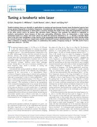
Design of Millimeter-Wave CMOS Radios: A Tutorial - UCLA ...
Design of Millimeter-Wave CMOS Radios: A Tutorial - UCLA ...
Design of Millimeter-Wave CMOS Radios: A Tutorial - UCLA ...

You also want an ePaper? Increase the reach of your titles
YUMPU automatically turns print PDFs into web optimized ePapers that Google loves.
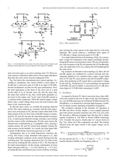
8 IEEE TRANSACTIONS ON CIRCUITS AND SYSTEMS—I: REGULAR PAPERS, VOL. 56, NO. 1, JANUARY 2009Fig. 6. Mixer reported in [2].Fig. 5. (a) Conventional active mixer, (b) active mixer using resonance andauxiliary current path, and (c) active topology with capacitive coupling.and conversion gain as an active topology does [7]. However,such a passive realization suffers from a lower input impedancethan does the active mixer, heavily loading the LNA.Fig. 5(a) shows the conventional active mixer topology. Accordingto simulations, this circuit exhibits a noise figure <strong>of</strong>26 dB and a conversion gain <strong>of</strong> 0 dB at an input <strong>of</strong> 60 GHz.Several mechanisms account for this poor performance. First,the total capacitance at the drain <strong>of</strong> gives rise to a poleon the order <strong>of</strong> . Second, since and must carrythe entire bias current <strong>of</strong> , they switch quite gradually, injectnoise to the output, and “waste” part <strong>of</strong> the RF current asa common-mode component. Third, the limited supply voltageallows only a small voltage drop across the load resistors andhence a low conversion gain.To alleviate these issues, we consider the topology depictedin Fig. 5(b), where inductor resonates with the total capacitanceseen at the drain <strong>of</strong> and also carries about half <strong>of</strong> thedrain current <strong>of</strong> [1]. Now, most <strong>of</strong> the RF current is commutatedby and because the equivalent parallel resistance<strong>of</strong> is much greater than the average resistance seen lookinginto the sources <strong>of</strong> the switching pair. (For the same reason, thethermal noise contributed by is negligible.) Also, carrying asmaller current, and switch more abruptly. Finally, theload resistors can be doubled. As a result, the noise figure fallsto about 18 dB and the conversion gain rises to 12 dB.Unfortunately, due to its small dimensions, transistorin Fig. 5(b) incurs a large mismatch with respect to , thuscreating substantial variations in the current flowing from theswitching pair. The topology depicted in Fig. 5(c) [44] avoidsthis issue by isolating the bias current <strong>of</strong> from that <strong>of</strong>the input transconductor. In this design, optimization <strong>of</strong> noisefigure and gain yields mA whereas mA,revealing that the conventional active mixer (with the switchingpair carrying the same current as the input device) is far fromoptimum. The circuit achieves a simulated noise figure <strong>of</strong>12.5 dB and a voltage conversion gain <strong>of</strong> 10.2 dB.As a single-balanced mixer, the topology <strong>of</strong> Fig. 5(c) can producea large LO component at the output, potentially desensitizingthe IF mixers in a heterodyne chain. The use <strong>of</strong> load inductorswith resonance at the IF can attenuate the LO feedthrough.Also, the small ratio <strong>of</strong> reduces the LO feedthrough bythe same factor.Fig. 6 depicts an alternative mixer topology [2]. Here, the LOand RF signals are combined by a passive network and subsequentlyapplied to two common-source stages. Large-signaldrive <strong>of</strong> and causes them to mix the LO and RF components,thus producing an IF current that is converted to voltageby the load . <strong>Design</strong>ed in 0.13- m technology for operationat 60 GHz, the mixer exhibits a conversion loss <strong>of</strong> 2 dB and anoise figure <strong>of</strong> 13.8 dB while consuming 2.4 mW.C. OscillatorsAs argued in Section IV, direct conversion faces three difficultissues related to the LO. In other words, the LO frequencyin a, say, 60-GHz radio may lie well below 60 GHz (Section VI).Nonetheless, it is beneficial to develop high-frequency oscillatorsfor future systems operating at hundreds <strong>of</strong> gigahertz.The oscillators reported in the literature for operation at60 GHz and above mostly employ a cross-coupled transistorpair with various resonator structures [4], [10], [13], [21], [45].We describe a different technique here that has led to fundamentaloscillation at 128 GHz in 90-nm <strong>CMOS</strong> technology[23]. Consider the passive fourth-order LC circuit shown inFig. 7(a), where all <strong>of</strong> the components are ideal. The transferfunction from the input current to the output voltage can beexpressed asFor the special case and , thetransfer function exhibits two imaginary poles at(2)(3)Authorized licensed use limited to: Univ <strong>of</strong> Calif Los Angeles. Downloaded on February 3, 2009 at 16:55 from IEEE Xplore. Restrictions apply.