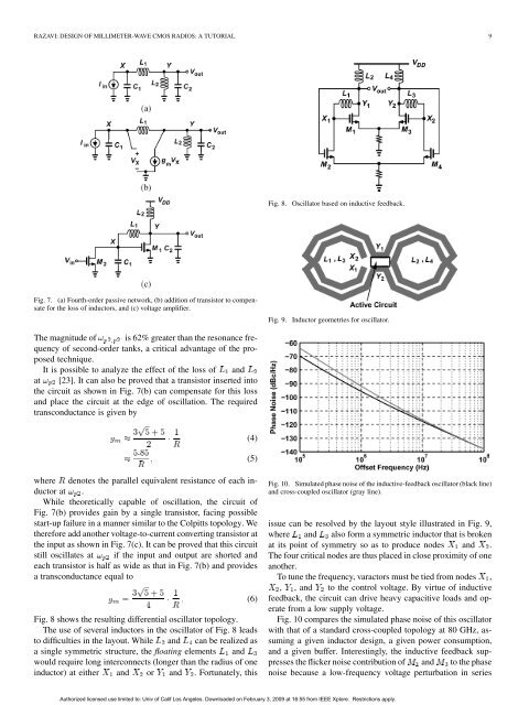
RAZAVI: DESIGN OF MILLIMETER-WAVE <strong>CMOS</strong> RADIOS: A TUTORIAL 9Fig. 8. Oscillator based on inductive feedback.Fig. 7. (a) Fourth-order passive network, (b) addition <strong>of</strong> transistor to compensatefor the loss <strong>of</strong> inductors, and (c) voltage amplifier.The magnitude <strong>of</strong> is 62% greater than the resonance frequency<strong>of</strong> second-order tanks, a critical advantage <strong>of</strong> the proposedtechnique.It is possible to analyze the effect <strong>of</strong> the loss <strong>of</strong> andat [23]. It can also be proved that a transistor inserted intothe circuit as shown in Fig. 7(b) can compensate for this lossand place the circuit at the edge <strong>of</strong> oscillation. The requiredtransconductance is given byFig. 9.Inductor geometries for oscillator.(4)(5)where denotes the parallel equivalent resistance <strong>of</strong> each inductorat .While theoretically capable <strong>of</strong> oscillation, the circuit <strong>of</strong>Fig. 7(b) provides gain by a single transistor, facing possiblestart-up failure in a manner similar to the Colpitts topology. Wetherefore add another voltage-to-current converting transistor atthe input as shown in Fig. 7(c). It can be proved that this circuitstill oscillates at if the input and output are shorted andeach transistor is half as wide as that in Fig. 7(b) and providesa transconductance equal toFig. 8 shows the resulting differential oscillator topology.The use <strong>of</strong> several inductors in the oscillator <strong>of</strong> Fig. 8 leadsto difficulties in the layout. While and can be realized asa single symmetric structure, the floating elements andwould require long interconnects (longer than the radius <strong>of</strong> oneinductor) at either and or and . Fortunately, this(6)Fig. 10. Simulated phase noise <strong>of</strong> the inductive-feedback oscillator (black line)and cross-coupled oscillator (gray line).issue can be resolved by the layout style illustrated in Fig. 9,where and also form a symmetric inductor that is brokenat its point <strong>of</strong> symmetry so as to produce nodes and .The four critical nodes are thus placed in close proximity <strong>of</strong> oneanother.To tune the frequency, varactors must be tied from nodes ,, , and to the control voltage. By virtue <strong>of</strong> inductivefeedback, the circuit can drive heavy capacitive loads and operatefrom a low supply voltage.Fig. 10 compares the simulated phase noise <strong>of</strong> this oscillatorwith that <strong>of</strong> a standard cross-coupled topology at 80 GHz, assuminga given inductor design, a given power consumption,and a given buffer. Interestingly, the inductive feedback suppressesthe flicker noise contribution <strong>of</strong> and to the phasenoise because a low-frequency voltage perturbation in seriesAuthorized licensed use limited to: Univ <strong>of</strong> Calif Los Angeles. Downloaded on February 3, 2009 at 16:55 from IEEE Xplore. Restrictions apply.
10 IEEE TRANSACTIONS ON CIRCUITS AND SYSTEMS—I: REGULAR PAPERS, VOL. 56, NO. 1, JANUARY 2009Fig. 11. Oscillator reported in [10].with the gate <strong>of</strong>, say, , cannot change the phase difference betweenand . Note that, for the new oscillator to operateat 80 GHz, it must be loaded with a much greater capacitancethan the load seen by the cross-coupled topology (as indicatedby the 62% speed advantage derived above).Fig. 11 shows an oscillator that addresses the issue <strong>of</strong> loadcapacitance presented by subsequent stages (e.g., frequency dividersor mixers) [10]. The circuit employs two transmissionlines <strong>of</strong> length equal to 3/4 <strong>of</strong> the wavelength. Differential operationestablishes a short-circuit termination at node , producingstanding waves with peak swings at nodes and andat and . With the load capacitance, , tied to the latternodes, rather than to the former, the maximum oscillation frequencyis increased substantially. Realized in 90-nm technologyand used in a 75-GHz PLL, the oscillator exhibits a phase noise<strong>of</strong> 88 dBs/Hz at 100-kHz <strong>of</strong>fset and consumes 8 mW [10].D. Frequency DividersDivide-by-two circuits have also kept up with oscillatorfrequencies. Flip-flop dividers [20], injection-locked topologies[3], [22], and Miller realizations [7], [23], [25] have beenreported.Frequency dividers must maintain proper speed and lockrange while satisfying many other exacting demands imposedby their environment: their input capacitance and requiredinput swings and common-mode level must be commensuratewith the oscillator’s output waveform; they must drive, withsufficient swings, the input capacitance <strong>of</strong> the next stage—anotherdivider (and IF mixers in a heterodyne receiver); and theymust avoid the use <strong>of</strong> input and output buffers as such bufferswould necessitate additional inductors, further complicatingthe distribution <strong>of</strong> signals.The circuit technique illustrated in Fig. 7(c) can also improvethe speed <strong>of</strong> frequency dividers. Shown in Fig. 12 is a Millertopology employing the inductive feedback configuration [23].The cross-coupled pair increases the loop gain and hence thelock range. Also, and form a differential “samplingmixer,” which presents less loading to the amplifier than conventionaldouble-balanced passive mixers. Specifically, the capacitanceat node switches periodically between and ina conventional mixer, thereby introducing a resistance betweenthese two nodes and lowering the gain <strong>of</strong> the amplifier. Here, onFig. 12.Fig. 13.Miller divider based on inductive-feedback amplifier.Basic heterodyne PLL.the other hand, the voltage is simply stored on the capacitancefor a half cycle (if and are sufficiently large).The circuit <strong>of</strong> Fig. 12 achieves high speeds even in 90-nm<strong>CMOS</strong> technology. Consuming 10.5 mW, three experimentalprototypes using different inductor designs exhibit the followinglock ranges: 88–104 GHz, 96–111 GHz, and 117–125 GHz.Heterodyne phase-locking is another candidate forhigh-speed dividers [9]. Depicted in Fig. 13 in its simplestform, a heterodyne PLL mixes the input with the VCO outputtimes, generating a frequency component at given by. If the circuit locks, this component must beequal to zero, and equal to . Other divide ratios canbe realized by inserting dividers in the feedback loop and/orat the input ports <strong>of</strong> the mixer [9]. A prototype realized in0.13- m <strong>CMOS</strong> technology operates from 64 to 70 GHz whileconsuming 6.5 mW.The use <strong>of</strong> consecutive mixers in a heterodyne PLL raises thepossibility <strong>of</strong> false lock due to unwanted mixing products. However,it can be shown that for divide ratios up to 4, the limitedVCO tuning range prohibits false lock [9].An example <strong>of</strong> mmW static dividers is shown in Fig. 14 [35].The circuit employs a flip-flop with class-AB clocking [36], thusachieving a lock range <strong>of</strong> 75 to 95 GHz while consuming 16 mWin 65-nm SOI technology.E. Power AmplifiersEfficient <strong>CMOS</strong> power amplifiers continue to challenge designerseven at lower frequencies. Recent work [37], [46] employscascaded common-source stages to deliver power levelsin the range <strong>of</strong> 10 to 12 dBm at 60 GHz. Fig. 15 shows anexample for operation at 77 GHz [37]. Using microstrips forboth matching and loads, the PA delivers a saturated output <strong>of</strong>6.3 dBm and draws 142 mW from a 1.2-V supply. The lackAuthorized licensed use limited to: Univ <strong>of</strong> Calif Los Angeles. Downloaded on February 3, 2009 at 16:55 from IEEE Xplore. Restrictions apply.