Design of Millimeter-Wave CMOS Radios: A Tutorial - UCLA ...
Design of Millimeter-Wave CMOS Radios: A Tutorial - UCLA ...
Design of Millimeter-Wave CMOS Radios: A Tutorial - UCLA ...

You also want an ePaper? Increase the reach of your titles
YUMPU automatically turns print PDFs into web optimized ePapers that Google loves.
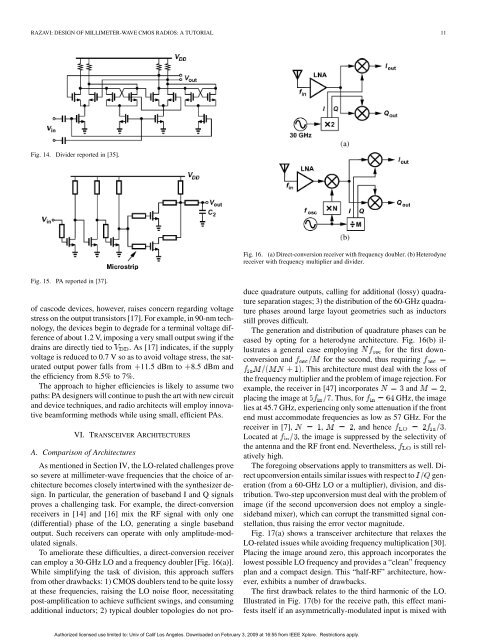
RAZAVI: DESIGN OF MILLIMETER-WAVE <strong>CMOS</strong> RADIOS: A TUTORIAL 11Fig. 14. Divider reported in [35].Fig. 16. (a) Direct-conversion receiver with frequency doubler. (b) Heterodynereceiver with frequency multiplier and divider.Fig. 15. PA reported in [37].<strong>of</strong> cascode devices, however, raises concern regarding voltagestress on the output transistors [17]. For example, in 90-nm technology,the devices begin to degrade for a terminal voltage difference<strong>of</strong> about 1.2 V, imposing a very small output swing if thedrains are directly tied to . As [17] indicates, if the supplyvoltage is reduced to 0.7 V so as to avoid voltage stress, the saturatedoutput power falls from 11.5 dBm to 8.5 dBm andthe efficiency from 8.5% to 7%.The approach to higher efficiencies is likely to assume twopaths: PA designers will continue to push the art with new circuitand device techniques, and radio architects will employ innovativebeamforming methods while using small, efficient PAs.VI. TRANSCEIVER ARCHITECTURESA. Comparison <strong>of</strong> ArchitecturesAs mentioned in Section IV, the LO-related challenges proveso severe at millimeter-wave frequencies that the choice <strong>of</strong> architecturebecomes closely intertwined with the synthesizer design.In particular, the generation <strong>of</strong> baseband I and Q signalsproves a challenging task. For example, the direct-conversionreceivers in [14] and [16] mix the RF signal with only one(differential) phase <strong>of</strong> the LO, generating a single basebandoutput. Such receivers can operate with only amplitude-modulatedsignals.To ameliorate these difficulties, a direct-conversion receivercan employ a 30-GHz LO and a frequency doubler [Fig. 16(a)].While simplifying the task <strong>of</strong> division, this approach suffersfrom other drawbacks: 1) <strong>CMOS</strong> doublers tend to be quite lossyat these frequencies, raising the LO noise floor, necessitatingpost-amplification to achieve sufficient swings, and consumingadditional inductors; 2) typical doubler topologies do not pro-for the first down-for the second, thus requiring. This architecture must deal with the loss <strong>of</strong>duce quadrature outputs, calling for additional (lossy) quadratureseparation stages; 3) the distribution <strong>of</strong> the 60-GHz quadraturephases around large layout geometries such as inductorsstill proves difficult.The generation and distribution <strong>of</strong> quadrature phases can beeased by opting for a heterodyne architecture. Fig. 16(b) illustratesa general case employingconversion andthe frequency multiplier and the problem <strong>of</strong> image rejection. Forexample, the receiver in [47] incorporates and ,placing the image at . Thus, for GHz, the imagelies at 45.7 GHz, experiencing only some attenuation if the frontend must accommodate frequencies as low as 57 GHz. For thereceiver in [7], , , and hence .Located at , the image is suppressed by the selectivity <strong>of</strong>the antenna and the RF front end. Nevertheless, is still relativelyhigh.The foregoing observations apply to transmitters as well. Directupconversion entails similar issues with respect to generation(from a 60-GHz LO or a multiplier), division, and distribution.Two-step upconversion must deal with the problem <strong>of</strong>image (if the second upconversion does not employ a singlesidebandmixer), which can corrupt the transmitted signal constellation,thus raising the error vector magnitude.Fig. 17(a) shows a transceiver architecture that relaxes theLO-related issues while avoiding frequency multiplication [30].Placing the image around zero, this approach incorporates thelowest possible LO frequency and provides a “clean” frequencyplan and a compact design. This “half-RF” architecture, however,exhibits a number <strong>of</strong> drawbacks.The first drawback relates to the third harmonic <strong>of</strong> the LO.Illustrated in Fig. 17(b) for the receive path, this effect manifestsitself if an asymmetrically-modulated input is mixed withAuthorized licensed use limited to: Univ <strong>of</strong> Calif Los Angeles. Downloaded on February 3, 2009 at 16:55 from IEEE Xplore. Restrictions apply.