Design of Millimeter-Wave CMOS Radios: A Tutorial - UCLA ...
Design of Millimeter-Wave CMOS Radios: A Tutorial - UCLA ...
Design of Millimeter-Wave CMOS Radios: A Tutorial - UCLA ...

Create successful ePaper yourself
Turn your PDF publications into a flip-book with our unique Google optimized e-Paper software.
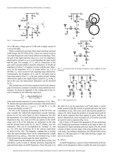
RAZAVI: DESIGN OF MILLIMETER-WAVE <strong>CMOS</strong> RADIOS: A TUTORIAL 7Fig. 2. Common-gate LNA.<strong>of</strong> 4.5 dB and a voltage gain <strong>of</strong> 12 dB with a supply current <strong>of</strong>4 mA at 60 GHz.While considered to provide robust input matching and gainin RF design, the CG LNA <strong>of</strong> Fig. 2 faces two serious issues atvery high frequencies and in deep submicron technology. First,the gate <strong>of</strong> the input transistor must see a very low-impedancereturn path to ground so as to avoid degrading the input matchand the gain. For example, if and its connections to thegate and to ground exhibit a parasitic inductance <strong>of</strong> 20 pH, animpedance <strong>of</strong> about appears in series with the gate. Moreover,for the impedance <strong>of</strong> to remain below, say, 5 at60 GHz, must exceed 0.5 pF, requiring large dimensions.Unfortunately, the footprints <strong>of</strong> and inevitably lead tolong interconnects from to the gate and/or ground. Similarobservations apply to the supply bypass capacitor in Fig. 2,but in this case, the interconnect inductance can be absorbedby .The second issue in CG LNAs manifests itself as the intrinsicgain <strong>of</strong> transistors continues to decline in deep submicron technologies.As shown in Appendix A, the voltage gain <strong>of</strong> the circuitis bounded by the following expression:Fig. 3. (a) Cascode LNA, (b) nesting <strong>of</strong> inductors, and (c) addition <strong>of</strong> seriesresonance.(1)if the input remains matched to a source impedance <strong>of</strong> . Here,denotes the equivalent parallel resistance <strong>of</strong> the drain tank atresonance. Thus, with and , thevoltage gain hardly exceeds 2.5.In view <strong>of</strong> the foregoing shortcomings <strong>of</strong> the CG LNA, onemay consider the inductively-degenerated cascode topology,known for its low noise figure at lower frequencies but alsothe dependence <strong>of</strong> its input matching upon package parasitics.Depicted in Fig. 3(a), such an LNA can operate in the mmWrange only if all <strong>of</strong> the inductors are integrated on the chipand the ground return paths for and display very lowinductance. This can be accomplished by “nesting” and[7], [43], thus localizing all <strong>of</strong> the critical connectionsas shown in Fig. 3(b). The magnetic coupling due to nestingalters the input matching, but it can be compensated by a slightadjustment <strong>of</strong> and . Note that one terminal <strong>of</strong> is tiedto the ground line located under the input signal line.While improving the stability, the cascode device in Fig. 3(a)introduces a pole at node , thereby adversely impacting thegain and noise figure at mmW frequencies. Since this pole is onFig. 4. LNA reported in [33].the order <strong>of</strong> , the capacitance at both shunts a considerableportion <strong>of</strong> the RF current to ground and raises the noisecontribution <strong>of</strong> . This issue can be alleviated by parallel resonance[7], while facing the problem <strong>of</strong> ground return path forthe dc block capacitor that must appear in series with the inductor.Alternatively, series resonance [5], [15] can be used withno need for such a capacitor [Fig. 3(c)].Fig. 4 shows a W-band LNA designed in 65-nm technology[33]. Employing transformer feedback at the input to allow optimizationfor input matching and noise figure [34], the circuitconsists <strong>of</strong> three cascode stages with series peaking at the cascodenodes. According to simulations, the LNA provides a noisefigure <strong>of</strong> 7 dB and a gain <strong>of</strong> 17 dB while drawing a supply current<strong>of</strong> 24 mA [33].B. MixersAt mmW frequencies, a passive mixer followed by an IF amplifiercan be designed to achieve roughly the same noise figureAuthorized licensed use limited to: Univ <strong>of</strong> Calif Los Angeles. Downloaded on February 3, 2009 at 16:55 from IEEE Xplore. Restrictions apply.