An FPGA-based SPWM Generator for High-Frequency DC/AC ...
An FPGA-based SPWM Generator for High-Frequency DC/AC ...
An FPGA-based SPWM Generator for High-Frequency DC/AC ...

Create successful ePaper yourself
Turn your PDF publications into a flip-book with our unique Google optimized e-Paper software.
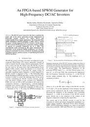
<strong>An</strong> <strong>FPGA</strong>-<strong>based</strong> <strong>SPWM</strong> <strong>Generator</strong> <strong>for</strong><strong>High</strong>-<strong>Frequency</strong> <strong>DC</strong>/<strong>AC</strong> InvertersMatina Lakka, Eftichios Koutroulis, Apostolos DollasDepartment of Electronic & Computer EngineeringTechnical University of CreteGR-73100, Chania, Greecematinalakka@gmail.com, efkout@electronics.tuc.gr, dollas@ece.tuc.grAbstract—The <strong>DC</strong>/<strong>AC</strong> power converters (inverters) constitute themajor unit of the power generation systems implemented inRenewable Energy Sources, <strong>AC</strong> motor drives andUninterruptible Power Supply applications. The Sinusoidal PulseWidth Modulation (<strong>SPWM</strong>) principle is widely used to controlthe power switches deployed in <strong>DC</strong>/<strong>AC</strong> inverters. In this paper,an <strong>FPGA</strong>-<strong>based</strong> SWPM generator is presented, which is capableto operate at switching frequencies up to 1 MHz. Theexperimental results presented in this paper demonstrate thesuperiority of the proposed SWPM architecture over its pastproposedcounterparts in terms of both the maximum operatingswitching frequency and the accuracy of reproducing the desired<strong>SPWM</strong> wave<strong>for</strong>m.I. INTRODUCTIONThe <strong>DC</strong>/<strong>AC</strong> power converters (inverters) are deployed in gridconnectedPhotoVoltaic (PV) power generation systems inorder to transfer the <strong>DC</strong> energy which is generated by the PVpower source into the <strong>AC</strong> electric grid. The <strong>DC</strong>/<strong>AC</strong> invertersare also used in <strong>AC</strong>-motor drive and Uninterruptible PowerSupply (UPS) systems, where the objective is to convert the<strong>DC</strong> input voltage into a sinusoidal <strong>AC</strong> output voltage ofadjustable magnitude and/or frequency. A block diagram of a<strong>DC</strong>/<strong>AC</strong> inverter is depicted in Fig. 1. The Sinusoidal PulseWidth Modulation (<strong>SPWM</strong>) principle is widely used in <strong>DC</strong>/<strong>AC</strong>inverters in order to control the operating state of the powerswitches constituting the <strong>DC</strong>/<strong>AC</strong> inverter structure. In thiscase, the power switches of the converter (e.g. MOSFETs,IGBTs etc.) are set ON or OFF according to the result of thecomparison between a high-frequency, constant-amplitudetriangular wave (carrier) with two low-frequency (e.g. 50 Hz)reference sine-waves of adjustable amplitude [1]. This processis illustrated in Fig. 2. By using the <strong>SPWM</strong> technique, theFigure 1. A diagram of a <strong>DC</strong>/<strong>AC</strong> power converter (inverter).Figure 2. The Sinusoidal Pulse Width Modulation (<strong>SPWM</strong>) principle.frequency spectrum of the <strong>DC</strong>/<strong>AC</strong> inverter output wave<strong>for</strong>m is<strong>for</strong>matted such that the non-fundamental harmonic componentsare located at relatively high frequencies (typically in the orderof several kHz). The high-frequency harmonics of thegenerated <strong>SPWM</strong> signal, Vspwm, are then filtered using a lowpassLC- or LCL-type filter, thus producing the high-powerand low-frequency sinusoidal wave<strong>for</strong>m, V , at the <strong>DC</strong>/<strong>AC</strong>inverter output terminals (Fig. 2). The amplitude ofcalculated as follows:oVois VcVo= M⋅V d= ⋅ Vd(1)Vwhere Vd(V) is the <strong>DC</strong> input voltage of the <strong>DC</strong>/<strong>AC</strong> inverter,Vc(V) and Vtr(V) are the amplitudes of the reference sine andcarrier waves, respectively and M is the modulation index.Increasing the frequency of the triangular wave (switchingfrequency), fc, results in an increase of the <strong>DC</strong>/<strong>AC</strong> inverterpower density due to the reduction of the volume of themagnetic components comprising the output filter.The control unit of the <strong>DC</strong>/<strong>AC</strong> inverter is used <strong>for</strong> theexecution of control and energy management algorithms (e.g.output voltage regulation, Maximum Power Point Tracking-MPPT, <strong>SPWM</strong> modulation strategies etc.) and it is developedusing microcontroller, DSP and <strong>FPGA</strong> ICs [2]. Compared totr
the implementation using analog circuits, digital controllersenable the implementation of advanced control algorithms,offer flexibility in case of changes and they are less susceptibleto component and ambient variations [3]. Nowadays, FieldProgrammable Gate Arrays (<strong>FPGA</strong>s) are extensively used tocontrol power electronic converters, such as <strong>DC</strong>/<strong>DC</strong>converters, matrix converters, resonant converters, converters<strong>for</strong> power factor correction applications and <strong>AC</strong>/<strong>DC</strong> converters[4]. In contrast to the microcontroller and DSP devices, <strong>FPGA</strong>sare able to execute the control operations concurrently, thusper<strong>for</strong>ming high-speed computations in real time. The adventof <strong>FPGA</strong> technology has enabled rapid prototyping of digitalsystems.Depending on their nominal power rating, the <strong>DC</strong>/<strong>AC</strong> inverterstypically operate at switching frequencies, fc, in the range of1-100 kHz [5, 6]. However, operation at higher switchingfrequencies is expected in the near future [7] due to theavailability of modern power semiconductor devices, such asSilicon Carbide (SiC) JFETs, which are able to operate atswitching frequencies up to 3 MHz with low power losses [8].The digital <strong>SPWM</strong> generation unit implementations havedominated over their counterparts <strong>based</strong> on analog circuits,since they offer higher noise immunity and less susceptibilityto voltage and temperature variations [9]. In this paper, an<strong>FPGA</strong>-<strong>based</strong> <strong>SPWM</strong> generator is presented, which is capableto operate at switching frequencies up to 1 MHz (requiring<strong>FPGA</strong> operation at 100-160MHz), thus it is capable to supportthe high switching frequency requirements of modern powerelectronic <strong>DC</strong>/<strong>AC</strong> converters. In the following sections of thispaper the architectures of past-proposed SWPM generationunits are analyzed, the proposed <strong>FPGA</strong>-<strong>based</strong> SWPMgenerator is presented and the experimental results arediscussed.II.PAST-PROPOSED <strong>SPWM</strong> GENERATOR ARCHITETCURESIn the <strong>FPGA</strong>-<strong>based</strong> <strong>SPWM</strong> generation units presented in[10-15], the triangular wave is implemented in the <strong>for</strong>m of anup-down counter. The reference sine-wave is sampled, with asampling frequency equal to f , at the time instants whichscorrespond either only to the nadirs or both at the nadirs andthe peaks of the carrier wave (Fig. 3). The correspondingsamples are stored in digital <strong>for</strong>mat in a Look-Up Table (LUT)implemented in the <strong>FPGA</strong> internal memory. The <strong>SPWM</strong>control signals are produced by comparing the correspondingvalues of the sinusoidal and carrier digital signals.The architecture presented in [12] implements an <strong>SPWM</strong>generator by sampling the sine-wave at the nadir times of thecarrier wave. This architecture was implemented on theXC4000XL Xilinx <strong>FPGA</strong> device with a 5 kHz switchingfrequency. The sine-wave used as a reference to generate the<strong>SPWM</strong> output is divided into four symmetric sections, i.e.sections A, B, C and D, respectively, in Fig. 4. Section Bcorresponds to the mirror of A, while sections C and D areequal to the opposites of sections A and B, respectively. Hence,sections B, C and D of the reference sine-wave can bereconstructed by storing data relevant to section A only. In thisway, only a quarter of the sine-wave period is required to bestored. This approach reduces representations to 25% of thetotal data required to re-produce the reference sine-wave. Theoverall block diagram of the <strong>SPWM</strong> generator proposed in [12]is shown in Fig. 5(a). The system consists of an eight-bit updowncounter which generates a triangular wave<strong>for</strong>m byincreasing its value from 0 to 255 and then subsequentlydecrementing it back to 0 over a period of time equal toTc= 1 / f . The resulting carrier signal is compared with thecoutput of the multiplier, which is obtained from multiplicationof the modulating signal produced using the look-up table data,as analyzed above, with an external modulation index input.The architecture proposed in [15] implements a three-phase<strong>FPGA</strong>-<strong>based</strong> <strong>SPWM</strong> generator by sampling the sine-wave bothat the nadir and the peak instants of the carrier-wave with a20 kHz switching frequency. The <strong>SPWM</strong> core has beendesigned using VHDL and implemented in a single <strong>FPGA</strong>device (SPARTAN XC3S400PQ208). The block diagram ofthis architecture is shown in Fig. 5(b). The reference sine-waveis generated by the “sine-wave generator” module using a lookuptable which contains the values of a sine-wave <strong>for</strong> 180°(half-period). The <strong>SPWM</strong> output pulses [i.e. signals PWM A,B and C in Fig. 5(b)] are generated by the “PWM Controller”module by comparing the sinusoidal reference and triangularcarrier signals. The QALU subsystem per<strong>for</strong>ms the dataFigure 4. The optimization concept of the <strong>SPWM</strong> generatorpresented in [12].(a)Figure 3. The operating principles of past-proposed <strong>SPWM</strong> generators.(b)Figure 5. Block diagrams of past-proposed <strong>SPWM</strong> generation units: (a)the architecture proposed in [12] an (b) the architecture proposed in [15].
epresentation as well as the arithmetic and logic operations ofthe <strong>SPWM</strong> algorithm in Q-Format representation.In [16, 17], the sampling frequency of the reference sine-wave,fs, is reduced by N in order to give a sampling frequency /carrier frequency relationship expressed by fs= 2 fc/ N . Thisprocedure results in only one sample being taken every N-samples of the conventional cases described above. Thus, thenumber of calculations required to produce the complete PWMwave<strong>for</strong>m is N times less than in the conventional cases. Thisis a substantial saving in calculation time, which enables todevelop <strong>SPWM</strong> generation units operating at significantlyhigher switching frequencies, <strong>for</strong> the same number ofcalculations per<strong>for</strong>med.<strong>An</strong>other approach that has been proposed is the one thatalthough it uses a look-up table to store the values of thereference sine-wave corresponding to the time instants of thetriangular wave peaks and nadirs, there is no comparisonper<strong>for</strong>med between the sine and the triangular waves [18, 19].In this case, the width of each pulse of the generated <strong>SPWM</strong>wave<strong>for</strong>m is derived by a calculation per<strong>for</strong>med according toan equation <strong>based</strong> on the similarity of two triangles ABC andADF that are <strong>for</strong>med between the sine and triangular (carrier)reference waves, as shown in Fig. 3.A common disadvantage of the past-proposed <strong>SPWM</strong>generators described above is that they have been designed tooperate at low switching frequencies (i.e. 1 kHz - 20 kHz),while their operation at higher switching frequencies has notbeen explored.III.THE PROPOSED <strong>FPGA</strong>-BASED <strong>SPWM</strong> GENERATORThe architecture of the proposed <strong>FPGA</strong>-<strong>based</strong> <strong>SPWM</strong>generation unit is illustrated in Fig. 6. Compared to the pastproposed<strong>SPWM</strong> generators, in the architecture proposed inthis paper the values of both the reference sine- and triangularwaves are stored in the BRAMs of the <strong>FPGA</strong> device, thusexploiting their one-clock-cycle access time. In order toproduce the discrete values used <strong>for</strong> the BRAMs initializationover the corresponding sampling period and simultaneouslyminimize the <strong>FPGA</strong> resource utilization, the memories areorganized such that both the sinusoidal and triangular wavesare sampled and quantized using the MATLAB software toolwith the same sampling frequency (e.g. 4 MHz, 16 MHz etc.).The proposed <strong>SPWM</strong> generation unit consists of five majorsubsystems. The input of the <strong>SPWM</strong> generator is themodulation index in single precision floating point arithmetic,while the system architecture is <strong>based</strong> on an 8-bit fixed-pointarithmetic. The “Clock <strong>Generator</strong>” subsystem takes as input thesystem clock and produces a new one that allows the wholesystem to operate in the desired switching frequency, fc. The“Modulation Index Module” accepts as input the modulationindex, which ranges from 0 to 1 and converts it to fixed-pointarithmetic, resulting in a fixed value ranging from 0 to 255.The “Sine-carrier” subsystem consists of the control unit, twoBRAMs, which store the values of the reference sinusoidal andtriangular signals, respectively, and two multiplexers whichproduce the two (positive and negative) reference sine-waves.The “Adjustable amplitude sine” subsystem outputs twosinusoidal digital signals with amplitude adjustable accordingto the value of the modulation index, which is also an input ofthis subsystem. The “Comparison” subsystem implements thecomparison between the high-frequency, constant-amplitudetriangular wave (carrier) with the two low-frequency referencesine-waves of adjustable amplitude, using two comparators.The control signals Ta+, Ta-, Tb+and Tb-of the <strong>DC</strong>/<strong>AC</strong>inverter power switches depicted in Fig. 1 are generated fromthe outputs of the corresponding comparators of thissubsystem, thus <strong>for</strong>ming the <strong>SPWM</strong> pattern, Vspwm, in Fig. 2.IV.EXPERIMENTAL RESULTSThe per<strong>for</strong>mance of the proposed <strong>SPWM</strong> generation systemhas been evaluated on an actual design, which has been fullyimplemented and downloaded to an <strong>FPGA</strong> board containingthe XC5VLX110T Virtex-5 Xilinx <strong>FPGA</strong> device. The XilinxISE Design Suite 10.1 tool was used <strong>for</strong> the design of thereconfigurable architecture. The oscilloscope measurement ofthe generated control signal Ta+( T a-, Tb+and Tb-are similarlyproduced) in case that fc= 1 kHz and M = 0.5 is illustratedin Fig. 7. It is observed that the frequency of the individualpulses is equal to the switching frequency of the <strong>SPWM</strong> wave.The Fast Fourier Trans<strong>for</strong>m (FFT) of the <strong>SPWM</strong> wave, whichemulates the Vspwmsignal depicted in Fig. 1 and it is producedby subtracting the Ta+and Tb+control signals generated by theproposed system, in case that fc= 1 MHz , fs= 4 MHz andM = 0.5 , is depicted in Fig. 8. It is observed that the unipolar<strong>SPWM</strong> scheme, where either positive or negative pulses areproduced within each half-period of the <strong>SPWM</strong> output wave[1], has the advantage of “effectively” doubling the switchingfrequency as far as the harmonics are concerned. Theadvantage of “effectively” doubling the switching frequencyFigure 7. The control signal Ta+in case that fc= 1 kHz and M = 0.5 .Figure 6. The architecture of the proposed <strong>FPGA</strong>-<strong>based</strong> <strong>SPWM</strong> generator.Figure 8. The FFT pattern of the generated <strong>SPWM</strong> output wave<strong>for</strong>m incase that f = 1 MHz , f = 4 MHz and M = 0.5 .cs
TABLE I. COMPARISON OF THE EXPERIMENTAL RESULTSOBTAINED BY THE PAST-PROPOSED <strong>SPWM</strong> ARCHITECTURES AND THEPROPOSED <strong>SPWM</strong> GENERATORMaximum switchingfrequencyModulation indexdeviation from itstheoretical value <strong>for</strong>f = 10 kHz andcM = 0.1-1Power consumption at themaximum operatingswitching frequencyDeviation of the TotalHarmonic Distortion(THD) of the generated<strong>SPWM</strong> wave<strong>for</strong>m fromits theoretical valueProposed <strong>SPWM</strong>generatorPast-proposed <strong>SPWM</strong>architectures1 MHz 0.25 MHzup to 5.6% up to 98.9%0.889 W(at 1MHz)0.887 - 0.932 W(at 10-250 kHz)7.3 % 7.7-26.8 %appears in the harmonic spectrum of the Vspwmoutput voltagewave<strong>for</strong>m, where the harmonics appear at sidebands which arelocated at multiples of twice the switching frequency, fc.The past-proposed <strong>SPWM</strong> generators presented in [12, 15-19]were also implemented in the same target Virtex-5 <strong>FPGA</strong>device in order to evaluate their per<strong>for</strong>mance and compare itwith that of the proposed SWPM generator. These architectureswere implemented such that they produce a unipolar <strong>SPWM</strong><strong>for</strong> single-phase full-bridge <strong>DC</strong>/<strong>AC</strong> inverters in order to befully compatible with the new <strong>SPWM</strong> generator introduced inthis paper. A comparison of the experimental results obtainedby the past-proposed <strong>SPWM</strong> generator architectures and theone proposed in this paper is summarized in Table I. In termsof the <strong>FPGA</strong> resources required, all architectures occupy asmall fraction (≈ 9 %) of the medium-sized <strong>FPGA</strong> device used.The BRAMs are the most critical resource that restricts anyfurther increase of the sampling frequency of the proposed<strong>SPWM</strong> generator architecture, while the next critical resourceis the DSPs that, compared to the past-proposed SWPMgeneration implementations, occupy 3% more space in the<strong>FPGA</strong> device.V. CONCLUSIONSThe <strong>SPWM</strong> principle is widely used to control the operation ofpower electronic <strong>DC</strong>/<strong>AC</strong> converters. The experimental resultspresented in this paper verify that the maximum operatingswitching frequency of the past-proposed <strong>FPGA</strong>-<strong>based</strong> <strong>SPWM</strong>generators does not exceed 250 kHz. In this paper, an <strong>FPGA</strong><strong>based</strong>SWPM generator has been presented, which is capable tooperate at switching frequencies up to 1 MHz, thus it is capableto support the high switching frequency requirements ofmodern power electronic <strong>DC</strong>/<strong>AC</strong> converters. In order to beable to achieve operation at switching frequencies up to 1 MHzrequires <strong>FPGA</strong> operation at 100-160 MHz. The successfuloperation of the proposed SWPM generator at high switchingfrequencies has been verified with experimental results onactual hardware, thus validating the design.REFERENCES[1] N. Mohan, T.M. Undeland, W.P. Robbins, “Power Electronics:Converters, Applications and Design”, Wiley, 3 rd Edition, 2002.[2] E. Koutroulis, F. Blaabjerg, “Design optimization of grid-connected PVinverters”, 2011 Twenty-Sixth <strong>An</strong>nual IEEE Applied Power ElectronicsConference and Exposition (APEC), pp. 691-698, 2011.[3] A.M. Omar, N.A. Rahim, “<strong>FPGA</strong>-<strong>based</strong> ASIC design of the three-phasesynchronous PWM flyback converter”, IEE-Proceedings Electric PowerApplications, Vol. 150, pp. 263-268, May 2003.[4] D. Hadiouche, L. Baghliand A. Rezzoug, “Space vector PWMtechniques <strong>for</strong> dual three-phase <strong>AC</strong> machine: analysis, per<strong>for</strong>mance,evaluation and DSP implementation”, IEEE Transactions on IndustryApplications, Vol. 42, No. 4, pp. 1112-1122, 2006.[5] Y. Hayashi, K. Takao, T. ShiMzu, H. Ohashi, “<strong>High</strong> power densitydesign methodology”, 2007 Power Conversion Conference, pp. 569-574,2007.[6] D. Floricau, G. Gateau, A. Leredde, R. Teodorescu, “The efficiency ofthree-level active NPC converter <strong>for</strong> different PWM strategies”, 13 thEuropean Conference on Power Electronics and Applications, pp. 1-9,2009.[7] R. Lai, F. Wang, P. Ning, D. Zhang, D. Jiang, R. Burgos, D.Boroyevich, K.J. KariM, V.D. Immanuel, “A high-power-densityconverter”, IEEE Industrial Electronics Magazine, Vol. 4, Issue 4, pp. 4-12, 2010.[8] K. Sheng, Y. Zhang, L. Yu, M. Su, J.H. Zhao, “<strong>High</strong>-frequencyswitching of SiC high-voltage LJFET”, IEEE Transactions on PowerElectronics, Vol. 24, No. 1, pp. 271-277, 2009.[9] B. J. Patella, A. Prodic, Art Zirger, D. Maksimovic, “<strong>High</strong>-frequencydigital PWM controller IC <strong>for</strong> <strong>DC</strong>–<strong>DC</strong> converters”, IEEE Transactionson Power Electronics, Vol. 18, No. 1, pp. 438-446, January 2003.[10] M.K. Hamzah, Z. Idris, A. Saparon, M.S. Yunos, “<strong>FPGA</strong> design ofsingle-phase matrix converter operating as a frequency changer”, IEEE2 nd International Power and Energy Conference, pp. 1124-1129, 2008.[11] S.Z. Mohammad Noor, M.K. Hamzah, A. Saparon, “Single-phase matrixconverter <strong>for</strong> inverter operation controlled using Xilinx <strong>FPGA</strong>”, IEEE2 nd International Power and Energy Conference, pp. 764-769, 2008.[12] M.S.N. Romli, Z. Idris, A. Saparon, M.K. Hamzah, “<strong>An</strong> area-efficientSinusoidal Pulse Width Modulation (<strong>SPWM</strong>) technique <strong>for</strong> Single-PhaseMatrix Converter (SPMC)”, 3 rd IEEE Conference on IndustrialElectronics and Applications, pp. 1163-1168, 2008.[13] H. Hussin, A. Saparon, M. Muhamad, M.D. Risin, “Sinusoidal PulseWidth Modulation (<strong>SPWM</strong>) design and implementation by focusing onreducing harmonic content”, 4 th Asia International Conference onMathematical/<strong>An</strong>alytical Modelling and Computer Simulation, pp. 620-623, 2010.[14] S.R.S. Raihan, N.A. Rahim, “Modeling of <strong>FPGA</strong>-<strong>based</strong> Pulse-WidthModulation <strong>for</strong> parallel three-phase <strong>AC</strong>/<strong>DC</strong> converters”, 2009International Conference <strong>for</strong> Technical Postgraduates, pp. 1-3, 2009.[15] R.K. Pongiannan, P. Selvabharathi, N. Yadaiah, “<strong>FPGA</strong> <strong>based</strong> threephasesinusoidal PWM VVVF controller”, 1 st International Conferenceon Electrical Energy Systems, pp. 34-39, 2011.[16] S.R. Bowes, D. Holliday, “Optimal regular-sampled PWM invertercontrol technique”, IEEE Transactions on Industrial Electronics, Vol.54, No. 3, pp. 1547-1559, June 2007.[17] S. R. Bowes, Y.S. Lai, “Investigation into optimising high switchingfrequency regular sampled PWM control <strong>for</strong> drives and static powerconverters”, IEE-Proceedings Electric Power Applications, Vol. 143,No. 4, July 1996.[18] Liu Jian, Yin Xianggen, Zhang Zhe, Xiong Qing, “A new three-levelNPC inverter <strong>based</strong> on phase individual <strong>DC</strong>-link circuit and high qualitydigital <strong>SPWM</strong> control technology”, International Conference onCommunications, Circuits and Systems, pp. 732-736, 2009.[19] Liu Jian, Yin Xianggen, Zhang Zhe, Xiong Qing, “Study on theory andkey technologies of full digital <strong>SPWM</strong> implementation <strong>for</strong> three-levelNeutral Point Clamped inverter”, International Conference onCommunications, Circuits and Systems, pp. 1287-1291, 2007.