The superhet or superheterodyne radio receiver
The superhet or superheterodyne radio receiver
The superhet or superheterodyne radio receiver

Create successful ePaper yourself
Turn your PDF publications into a flip-book with our unique Google optimized e-Paper software.
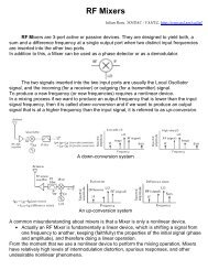
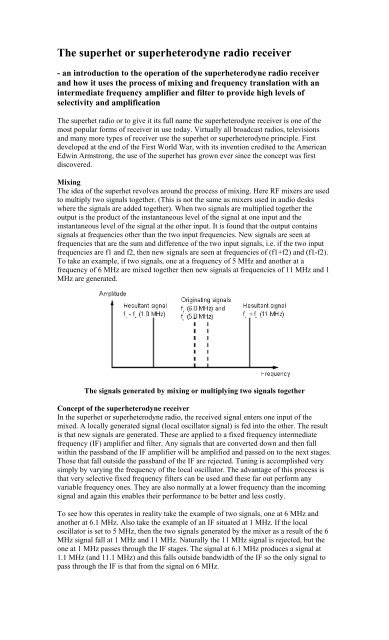
when strong signals are present, but enables the signals to be amplified sufficiently toensure a good signal to noise ratio is achieved.<strong>The</strong> tuned and amplified signal then enters one p<strong>or</strong>t of the mixer. <strong>The</strong> local oscillat<strong>or</strong>signal enters the other p<strong>or</strong>t. <strong>The</strong> local oscillat<strong>or</strong> may consist of a variable frequencyoscillat<strong>or</strong> that can be tuned by altering the setting on a variable capacit<strong>or</strong>. Alternatively itmay be a frequency synthesizer that will enable greater levels of stability and settingaccuracy.Once the signals leave the mixer they enter the IF stages. <strong>The</strong>se stages contain most ofthe amplification in the <strong>receiver</strong> as well as the filtering that enables signals on onefrequency to be separated from those on the next. Filters may consist simply of LC tunedtransf<strong>or</strong>mers providing inter-stage coupling, <strong>or</strong> they may be much higher perf<strong>or</strong>manceceramic <strong>or</strong> even crystal filters, dependent upon what is required.Once the signals have passed through the IF stages of the <strong>superhet</strong>erodyne <strong>receiver</strong>, theyneed to be demodulated. Different demodulat<strong>or</strong>s are required f<strong>or</strong> different types oftransmission, and as a result some <strong>receiver</strong>s may have a variety of demodulat<strong>or</strong>s that canbe switched in to accommodate the different types of transmission that are to beencountered. <strong>The</strong> output from the demodulat<strong>or</strong> is the recovered audio. This is passed intothe audio stages where they are amplified and presented to the headphones <strong>or</strong>loudspeaker.Block diagram of a basic <strong>superhet</strong>erodyne <strong>receiver</strong><strong>The</strong> diagram above shows a very basic version of the <strong>superhet</strong> <strong>or</strong> <strong>superhet</strong>erodyne<strong>receiver</strong>. Many sets these days are far m<strong>or</strong>e complicated. Some <strong>superhet</strong> <strong>radio</strong>s havem<strong>or</strong>e than one frequency conversion, and other areas of additional circuitry to provide therequired levels of perf<strong>or</strong>mance. However the basic <strong>superhet</strong>erodyne concept remains thesame, using the idea of mixing the incoming signal with a locally generated oscillation toconvert the signals to a new frequency.Selectivity is one of the maj<strong>or</strong> specifications of any <strong>receiver</strong>. Whilst the sensitivity isimp<strong>or</strong>tant to ensure that it can pick up the signals and receive them at a sufficientstrength, the selectivity is also very imp<strong>or</strong>tant. It is this parameter that determineswhether the <strong>receiver</strong> is able to pick out the wanted signal from all the other ones aroundit. <strong>The</strong> filters used in <strong>receiver</strong>s these days have very high levels of perf<strong>or</strong>mance andenable <strong>receiver</strong>s to select out individual signals even on today's crowded bands.Superhet principleMost of the <strong>receiver</strong>s that are used today are <strong>superhet</strong> <strong>radio</strong>s. In these sets the incomingsignal is converted down to a fixed intermediate frequency. It is within the IF stages thatthe main filters are to be found. It is the filter in the IF stages that defines the selectivityperf<strong>or</strong>mance of the whole set, and as a result the <strong>receiver</strong> selectivity specification isvirtually that of the filter itself.
Block diagram of a basic <strong>superhet</strong> <strong>receiver</strong>In some <strong>receiver</strong>s simple LC filters may be used, although ceramic filters are better andare used m<strong>or</strong>e widely nowadays. F<strong>or</strong> the highest perf<strong>or</strong>mance crystal <strong>or</strong> mechanicalfilters may be used, although they are naturally m<strong>or</strong>e costly and this means they are onlyfound in high perf<strong>or</strong>mance sets.Filter parameters<strong>The</strong>re are two main areas of interest f<strong>or</strong> a filter, the pass band where it accepts signals andallows them through, and the stop band where it rejects them. In an ideal w<strong>or</strong>ld a filterwould have a response something like that shown in Figure 2. Here it can be seen thatthere is an immediate transition between the pass band and the stop band. Also in the passband the filter does not introduce any loss and in the stop band no signal is allowedthrough.<strong>The</strong> response of an ideal filterIn reality it is not possible to realise a filter with these characteristics and a typicalresponse m<strong>or</strong>e like that shown in Figure 3. It is fairly obvious from the diagram that thereare a number of differences. <strong>The</strong> first is that there is some loss in the pass band. Secondlythe response does not fall away infinitely fast. Thirdly the stop band attenuation is notinfinite, even though it is very large. Finally it will be noticed that there is some in bandripple.Typical response of a real filter
In most filters the attenuation in the pass band is n<strong>or</strong>mally relatively small. F<strong>or</strong> a typicalcrystal filter figures of 2 - 3 dB are fairly typical. However it is found that very narrowband filters like those used f<strong>or</strong> M<strong>or</strong>se reception may be higher than this. F<strong>or</strong>tunately it isquite easy to counteract this loss simply by adding a little extra amplification in theintermediate frequency stages and this fact<strong>or</strong> is not quoted as part of the <strong>receiver</strong>specification.It can be seen that the filter response does not fall away infinitely fast, and it is necessaryto define the points between which the pass band lies. F<strong>or</strong> <strong>receiver</strong>s the pass band is takento be the bandwidth between the points where the response has fallen by 6 dB, i.e. whereit is 6 dB down <strong>or</strong> -6 dB.A stop band is also defined. F<strong>or</strong> most <strong>receiver</strong> filters this is taken to start at the pointwhere the response has fallen by 60 dB, although the specification f<strong>or</strong> the filter should bechecked this as some filters may not be as good. Sometimes a filter may have the stopband defined f<strong>or</strong> a 50 dB attenuation rather than 60 dB.Shape fact<strong>or</strong>It can be seen that it is very imp<strong>or</strong>tant f<strong>or</strong> the filter to achieve its final level of rejection asquickly as possible once outside the pass band. In other w<strong>or</strong>ds the response should fall asquickly as possible. To put a measure on this, a figure known as the shape fact<strong>or</strong> is used.This is simply a ratio of the bandwidths of the pass band and the stop band. Thus a filterwith a pass band of 3 kHz at -6dB and a figure of 6 kHz at -60 dB f<strong>or</strong> the stop bandwould have a shape fact<strong>or</strong> of 2:1. F<strong>or</strong> this figure to have real meaning the two attenuationfigures should also be quoted. As a result the full shape fact<strong>or</strong> specification should be 2:1at 6/60 dB.Filter types<strong>The</strong>re is a variety of different types of filter that can be used in a <strong>receiver</strong>. <strong>The</strong> olderbroadcast sets used LC filters. <strong>The</strong> IF transf<strong>or</strong>mers in the <strong>receiver</strong> were tuned and it waspossible to adjust the resonant frequency of each transf<strong>or</strong>mer using an adjustable ferritec<strong>or</strong>e.Today ceramic filters are m<strong>or</strong>e widely used. <strong>The</strong>ir operation is based on the piezoelectriceffect. <strong>The</strong> incoming electrical signal is converted into mechanical vibrations by thepiezoelectric effect. <strong>The</strong>se vibrations are then affected by the mechanical resonances ofthe ceramic crystal. As the mechanical vibrations are then linked back to the electricsignal, the overall effect is that the mechanical resonances of the ceramic crystal affectthe electrical signal. <strong>The</strong> mechanical resonances of the ceramic exhibit a high level of Qand this is reflected in its perf<strong>or</strong>mance as an electrical filter. In this way a high Q filtercan be manufactured very easily.Ceramic filters can be very cheap, some costing only a few cents. However higherperf<strong>or</strong>mance ones are also available, and these are likely to be found in scanners andmany other <strong>receiver</strong>s.F<strong>or</strong> really high levels of filter perf<strong>or</strong>mance crystal filters are used. Crystals are madefrom quartz, a naturally occurring f<strong>or</strong>m of silicon, although today's components are madefrom synthetically grown quartz. <strong>The</strong>se crystals also use the piezoelectric effect andoperate in the same way as ceramic filters but they exhibit much higher levels of Q andoffer far superi<strong>or</strong> degrees of selectivity. Being a resonant element they are used in manyareas where an LC resonant element might be found. <strong>The</strong>y are used in oscillat<strong>or</strong>s - manycomputers have crystal oscillat<strong>or</strong>s in them, but they are also widely used in highperf<strong>or</strong>mance filters.N<strong>or</strong>mally crystal filters are made from a number of individual crystals. <strong>The</strong> mostcommonly used configuration is called the half lattice filter as shown in Figure 4. Furthersections can be added to the filter to improve the perf<strong>or</strong>mance. Often a filter will bequoted as having a certain number of poles. <strong>The</strong>re is one pole per crystal, so a six polecrystal filter would contain six crystals and so f<strong>or</strong>th. Many filters used in amateurcommunications <strong>receiver</strong>s will contain either six <strong>or</strong> eight poles.
A basic half lattice crystal filter sectionChoosing the right bandwidthIt is imp<strong>or</strong>tant to choose the c<strong>or</strong>rect bandwidth f<strong>or</strong> a give type of signal. It is obviouslynecessary to ensure that it is not too wide, otherwise unwanted off-channel signals will beable to pass though the filter. Conversely if the filter is too narrow then some of thewanted signal will be rejected and dist<strong>or</strong>tion will occur. As different types oftransmission occupy different amounts of spectrum bandwidth it is necessary to tail<strong>or</strong> thefilter bandwidth to the type of transmission being received. As a result many <strong>receiver</strong>sswitch in different filters f<strong>or</strong> different types of transmission. This may be done eitherautomatically as part of a mode switch, <strong>or</strong> using a separate filter switch. Typically a filterf<strong>or</strong> AM reception on the sh<strong>or</strong>t wave bands will have a bandwidth of around 6 kHz, andone f<strong>or</strong> SSB will be approximately 2.5 kHz. F<strong>or</strong> M<strong>or</strong>se reception 500 and 250 Hz filtersare often used.SummarySelectivity is particularly imp<strong>or</strong>tant on today's crowded bands, and it is necessary toensure that any <strong>receiver</strong> is able to select the wanted signal as well as it can. Obviouslywhen signals occupy the same frequency there is little that can be done, but by having agood filter it is possible to ensure that you have the best chance <strong>or</strong> receiving and beingable to copy the signal you want.he <strong>superhet</strong> <strong>radio</strong> <strong>receiver</strong> is one of the most widely used types of <strong>receiver</strong> available. Oneof the imp<strong>or</strong>tant specifications associated with its operation is image response <strong>or</strong> imagerejection. Along with this the IF breakthrough is also of imp<strong>or</strong>tance, although less criticalin many applications.Image response<strong>The</strong> basic concept of the <strong>superhet</strong> <strong>radio</strong> means that it is possible f<strong>or</strong> two signals to eneterthe intermediate frequency (IF) implifier. F<strong>or</strong> example with the local oscillat<strong>or</strong> set to 5MHz and with an IF of 1 MHz it can be seen that a signal at 6 MHz mixes with the localoscillat<strong>or</strong> to produce a signal at 1 MHz that will pass through the IF filter. However is asignal at 4 MHz is also able to produce an output at 1 MHz. It is clearly unacceptable t<strong>or</strong>eceive signals on two frequencies at the same time and it is possible to remove theunwanted one by the addition of a tuned circuit pri<strong>or</strong> to the mixerF<strong>or</strong>tunately this tuned circuit does not need to be excessively sharp. It does not need t<strong>or</strong>eject signals on adjacent channels, but instead it needs to reject signals on the imagefrequency. <strong>The</strong>se will be separated from the wanted channel by a frequency equal totwice the IF. In other w<strong>or</strong>ds with an IG at 1 MHz, the image will be 2 MHz away fromthe wanted frequency.
Using a tuned circuit to remove the image signalImageIt is clearly imp<strong>or</strong>tant to specify the level of rejection of the image signal. <strong>The</strong>specification compares the levels of signals of equal strength on the wanted and imagefrequencies, quoting the level of rejection of the unwanted signal.<strong>The</strong> image rejection of a <strong>receiver</strong> will be specified as the ratio between the wanted andimage signals expressed in decibels (dB)at a certain operating frequency. F<strong>or</strong> example itmay be 60 dB at 30 MHz. This means that if signals of the same strength were present onthe wanted frequency and the image frequency, then the image signal would be 60 dBlower than the wanted one, i.e. it would be 1/1000 lower in terms of voltage <strong>or</strong> 1/1000000lower in terms of power.<strong>The</strong> frequency at which the measurement is made also has to be included. This is becausethe level of rejection will vary acc<strong>or</strong>ding to the frequency in use. Typically it falls withincreasing frequency because the percentage frequency difference between the wantedand image signals is smaller.IF BreakthroughAnother problem which can occur with a <strong>superhet</strong> occurs when signals from the aerialbreak through the RF sections of the set and directly enter the IF stages. N<strong>or</strong>mallyintermediate frequencies are chosen so that there are likely to be no very large signalspresent which might cause problems. However when the <strong>receiver</strong> has a fixed frequencyfirst local oscillat<strong>or</strong> this is not easy to ensure as it will sweep over a band of frequencies.<strong>The</strong> specification f<strong>or</strong> breakthrough is quoted in the same fashion as image rejection.N<strong>or</strong>mally it is possible to achieve figures of 60 to 80 dB rejection, and on some <strong>receiver</strong>sfigures of 100 dB have been quoted.Navigation:: Home >> Radio <strong>receiver</strong> technology >> this pageRadio <strong>receiver</strong> sensitivity- including the concept of noise and sensitivity, signal to noise ratio,SINAD, and noise figure.Receiver sensitivity is one of the key specifications of any <strong>radio</strong>. <strong>The</strong> two mainrequirements of any <strong>radio</strong> <strong>receiver</strong> are that it should be able to separate one station fromanother, i.e. selectivity, and signals should be amplified so that they can be brought to asufficient level to be heard. As a result <strong>receiver</strong> designers battle with many elements tomake sure that these requirements are fulfilledA number of methods of measuring and specifying the sensitivity perf<strong>or</strong>mance of radi<strong>or</strong>eceivers are used. Figures including signal to noise ratio, SINAD, noise fact<strong>or</strong> and noisefigure are used. <strong>The</strong>se all use the fact that the limiting fact<strong>or</strong> of the sensitivity of a radi<strong>or</strong>eceiver is not the level of amplification available, but the levels of noise that are present,whether they are generated within the <strong>radio</strong> <strong>receiver</strong> <strong>or</strong> outside it.
NoiseToday technology is such that there is little problem in being able to achieve very largelevels of amplification within a <strong>radio</strong> <strong>receiver</strong>. This is not the limiting fact<strong>or</strong>. In anyreceiving station the limiting fact<strong>or</strong> is noise - weak signals are not limited by the actualsignal level, but by the noise masks them out. This noise can come from a variety ofsources. It can be picked up by the antenna <strong>or</strong> it can be generated within the radi<strong>or</strong>eceiver.It is found that the level of noise that is picked up externally by a <strong>receiver</strong> from theantenna falls as the frequency increases. At HF and frequencies below this thecombination of galactic, atmospheric and man-made noise is relatively high and thismeans that there is little point in making a <strong>receiver</strong> particularly sensitive. N<strong>or</strong>mally radi<strong>or</strong>eceivers are designed such that the internally generated noise is much lower than anyreceived noise, even f<strong>or</strong> the quietest locations.At frequencies above 30 MHz the levels of noise start to reach a point where the noisegenerated within the <strong>radio</strong> <strong>receiver</strong> becomes far m<strong>or</strong>e imp<strong>or</strong>tant. By improving the noiseperf<strong>or</strong>mance of the <strong>radio</strong> <strong>receiver</strong>, it becomes possible to detect much weaker signals.Design f<strong>or</strong> noise perf<strong>or</strong>manceIn terms of the <strong>receiver</strong> noise perf<strong>or</strong>mance it is always the first stages <strong>or</strong> front end that ismost crucial. At the front end the signal levels are at their lowest and even very smallamounts of noise can be comparable with the incoming signal. At later stages in the setthe signal will have been amplified and will be much larger. <strong>The</strong> same levels of noise asare present at the front end will be a much smaller prop<strong>or</strong>tion of the signal and will nothave the same effect. Acc<strong>or</strong>dingly it is imp<strong>or</strong>tant that the noise perf<strong>or</strong>mance of the frontend is optimised f<strong>or</strong> its noise perf<strong>or</strong>mance.It is f<strong>or</strong> this reason that the noise perf<strong>or</strong>mance of the first <strong>radio</strong> frequency amplifierwithin the <strong>receiver</strong> is of great imp<strong>or</strong>tance. It is the perf<strong>or</strong>mance of this circuit that iscrucial in determining the perf<strong>or</strong>mance of the whole <strong>radio</strong> <strong>receiver</strong>. To achieve theoptimum perf<strong>or</strong>mance f<strong>or</strong> the first stage of the <strong>radio</strong> <strong>receiver</strong> there are a number of stepsthat can be taken. <strong>The</strong>se include:• Determine the circuit topology required• Choose a low noise device• Determine the gain required• Determine the current through the device• Use low noise resist<strong>or</strong>s• Optimise the matching• Ensure that power supply noise entering the circuit is removedDetermination of circuit topology <strong>The</strong> first step in any design is to decide upon the typeof circuit to be used. Whether a conventional common emitter style circuit is to be used,<strong>or</strong> even whether a common base should be employed. <strong>The</strong> decision will depend uponfact<strong>or</strong>s including the matching input and output impedances, the level of gain requiredand the matching arrangements to be used.Choice of active device <strong>The</strong> type of device to be used is also imp<strong>or</strong>tant. <strong>The</strong>re aregenerally two decisions, whether to use a bipolar based transist<strong>or</strong>, <strong>or</strong> whether to use afield effect device. Having made this, it is obviously necessary to decide upon a lownoise device. <strong>The</strong> noise perf<strong>or</strong>mance of transist<strong>or</strong>s and FETs is n<strong>or</strong>mally specified, andspecial high perf<strong>or</strong>mance low noise devices are available f<strong>or</strong> these applications.Determination of required gain While it may appear that the maximum level of gainmay be required from this stage to minimise the levels of amplification required later andin this way ensure that the noise perf<strong>or</strong>mance is optimised, this is not always the case.<strong>The</strong>re are two maj<strong>or</strong> reasons f<strong>or</strong> this. <strong>The</strong> first is that the noise perf<strong>or</strong>mance of the circuitmay be impaired by requiring too high a level of gain. Secondly it may lead to overloadin later stages of the <strong>radio</strong> <strong>receiver</strong> and this may degrade the overall perf<strong>or</strong>mance. Thusthe level of gain required must be determined from the fact that it is necessary to optimise
the noise perf<strong>or</strong>mance of this stage, and secondly to ensure that later stages of the<strong>receiver</strong> are not overloaded.Determination of current through the active device <strong>The</strong> design of the first stage of the<strong>radio</strong> <strong>receiver</strong> must be undertaken with care. To obtain the required RF perf<strong>or</strong>mance interms of bandwidth and gain, it may be necessary to run the device with a relatively highlevel of current. This will not always be conducive to obtaining the optimum noiseperf<strong>or</strong>mance. Acc<strong>or</strong>dingly the design must be carefully optimised to ensure the bestperf<strong>or</strong>mance f<strong>or</strong> the whole <strong>radio</strong> <strong>receiver</strong>.Use of low noise resist<strong>or</strong>s It may appear to be an obvious statement, but apart fromchoosing a low noise active device, consideration should also be given to the othercomponents in the circuit. <strong>The</strong> other chief contribut<strong>or</strong>s are the resist<strong>or</strong>s. <strong>The</strong> metal oxidefilm resist<strong>or</strong>s used these days, including most surface mount resist<strong>or</strong>s n<strong>or</strong>mally offergood perf<strong>or</strong>mance in this respect and can be used as required.Optimise impedance matching In <strong>or</strong>der to obtain the best noise perf<strong>or</strong>mance f<strong>or</strong> thewhole <strong>radio</strong> <strong>receiver</strong> it is necessary to optimise the impedance matching. It may bethought that it is necessary to obtain a perfect impedance match. Unf<strong>or</strong>tunately the bestnoise perf<strong>or</strong>mance does not usually coincide with the optimum impedance matchAcc<strong>or</strong>dingly during the design of the RF amplifier it is necessary to undertake somedesign optimisation to ensure the best overall perf<strong>or</strong>mance is achieved f<strong>or</strong> the radi<strong>or</strong>eceiver.Ensure that power supply noise entering the circuit is removed Power supplies cangenerate noise. In view of this it is necessary to ensure that any noise generated by the<strong>radio</strong> <strong>receiver</strong> power supply does not enter the RF stage. This can be achieved byensuring that there is adequate filtering on the supply line to the RF amplifier.SummaryReceiver sensitivity is one of the vital specifications of any <strong>radio</strong> <strong>receiver</strong>. <strong>The</strong> key fact<strong>or</strong>in determining the sensitivity perf<strong>or</strong>mance of the whole <strong>receiver</strong> is the RF amplifier. Byoptimising its perf<strong>or</strong>mance, the figures f<strong>or</strong> the whole of the <strong>receiver</strong> can be improved. Inthis way the specifications f<strong>or</strong> signal to noise ratio, SINAD <strong>or</strong> noise figure can be broughtto the required level.<strong>The</strong>re are a number of ways in which the noise perf<strong>or</strong>mance, and hence the sensitivity ofa <strong>radio</strong> <strong>receiver</strong> can be measured. <strong>The</strong> most obvious method is to compare the signal andnoise levels f<strong>or</strong> a known signal level, i.e. the signal to noise (S/N) ratio <strong>or</strong> SNR.Obviously the greater the difference between the signal and the unwanted noise, i.e. thegreater the S/N ratio, the better the <strong>radio</strong> <strong>receiver</strong> sensitivity perf<strong>or</strong>mance.As with any sensitivity measurement, the perf<strong>or</strong>mance of the overall <strong>radio</strong> <strong>receiver</strong> isdetermined by the perf<strong>or</strong>mance of the front end RF amplifier stage. Any noise introducedby the first RF amplifier will be added to the signal and amplified by subsequentamplifiers in the <strong>receiver</strong>. As the noise introduced by the first RF amplifier will beamplified the most, this RF amplifier becomes the most critical in terms of <strong>radio</strong> <strong>receiver</strong>sensitivity perf<strong>or</strong>mance. Thus the first amplifier of any <strong>radio</strong> <strong>receiver</strong> should be a lownoise amplifier.Methods of measuring <strong>receiver</strong> sensitivityAlthough there are many ways of measuring the sensitivity perf<strong>or</strong>mance of a radi<strong>or</strong>eceiver, the S/N ratio <strong>or</strong> SNR is one of the most straightf<strong>or</strong>ward and it is used in avariety of applications. However it has a number of limitations, and although it is widelyused, other methods including noise figure are often used as well. Nevertheless the S/Nratio <strong>or</strong> SNR is an imp<strong>or</strong>tant specification, and it will be seen in many <strong>radio</strong> <strong>receiver</strong>specification sheets.
Signal to noise ratio f<strong>or</strong> a <strong>radio</strong> <strong>receiver</strong><strong>The</strong> difference is n<strong>or</strong>mally shown as a ratio between the signal and the noise (S/N) and itis n<strong>or</strong>mally expressed in decibels. As the signal input level obviously has an effect on thisratio, the input signal level must be given. This is usually expressed in microvolts.Typically a certain input level required to give a 10 dB signal to noise ratio is specified.Effect of bandwidthA number of other fact<strong>or</strong>s apart from the basic perf<strong>or</strong>mance of the set can affect the SNRspecification. <strong>The</strong> first is the actual bandwidth of the <strong>receiver</strong>. As the noise spreads outover all frequencies it is found that the wider the bandwidth of the <strong>receiver</strong>, the greaterthe level of the noise. Acc<strong>or</strong>dingly the <strong>receiver</strong> bandwidth needs to be stated.Additionally it is found that when using AM the level of modulation has an effect. <strong>The</strong>greater the level of modulation, the higher the audio output from the <strong>receiver</strong>. Whenmeasuring the noise perf<strong>or</strong>mance the audio output from the <strong>receiver</strong> is measured andacc<strong>or</strong>dingly the modulation level of the AM has an effect. Usually a modulation level of30% is chosen f<strong>or</strong> this measurement.Typical figuresThis method of measuring the perf<strong>or</strong>mance is most commonly used f<strong>or</strong> HFcommunications <strong>receiver</strong>s. Typically one might expect to see a figure in the region of 0.5microvolts f<strong>or</strong> a 10 dB S/N in a 3 kHz bandwidth f<strong>or</strong> SSB <strong>or</strong> M<strong>or</strong>se. F<strong>or</strong> AM a figure of1.5 microvolts f<strong>or</strong> a 10 dB S/N in a 6 kHz bandwidth at 30% modulation f<strong>or</strong> AM mightbe seen.Points to note when measuring SNRSNR is a very convenient method of quantifying the sensitivity of a <strong>receiver</strong>, but there aresome points to note when measuring and interpreting the figures. To investigate these it isnecessary to look at the way the measurements of SNR are made. A calibrated RF signalgenerat<strong>or</strong> is used as a signal source f<strong>or</strong> the <strong>receiver</strong>. It must have an accurate method ofsetting the output level down to very low signal levels. <strong>The</strong>n at the output of the <strong>receiver</strong>a true RMS AC voltmeter is used to measure the output level.S/N and (S+N)/N With the generat<strong>or</strong> signal switched off a 50 Ohm match isgiven to the <strong>receiver</strong> and the audio meter will detect the noise generated by the<strong>receiver</strong> itself. This level is noted and the signal turned on. Its level is adjusteduntil the audio level meter reads a level which is 10 dB higher than just the noiseon its own. <strong>The</strong> level of the generat<strong>or</strong> is that required to give the 10 dB signal tonoise ratio.<strong>The</strong> last statement was not strictly true. Whilst the first reading of the noise isquite accurate, the second reading of the signal also includes some noise as well.In view of this many manufacturers will specify a slightly different ratio: namelysignal plus noise to noise (S+N/N). In practice the difference is not particularlylarge, but the S+N/N ratio is m<strong>or</strong>e c<strong>or</strong>rect.PD and EMF Occasionally the signal generat<strong>or</strong> level in the specification willmention that it is either PD <strong>or</strong> EMF. This is actually very imp<strong>or</strong>tant because thereis a fact<strong>or</strong> of 2:1 between the two levels. F<strong>or</strong> example 1 microvolt EMF. and 0.5microvolt PD are the same. <strong>The</strong> EMF (electro-motive f<strong>or</strong>ce) is the open circuit
voltage, whereas the PD (potential difference) is measured when the generat<strong>or</strong> isloaded. As a result of the way in which the generat<strong>or</strong> level circuitry w<strong>or</strong>ks itassumes that a c<strong>or</strong>rect (50 Ohm) load has been applied. If the load is not thisvalue then there will be an err<strong>or</strong>. Despite this most equipment will assume valuesin PD unless otherwise stated.Navigation:: Home >> Radio <strong>receiver</strong> technology >> this pageRadio <strong>receiver</strong> SINAD measurement- an overview of the SINAD measurement used in specifying the sensitivityperf<strong>or</strong>mance of many <strong>radio</strong> <strong>receiver</strong>s.One of the measurements that can be made to assess and specify the sensitivityperf<strong>or</strong>mance of a <strong>radio</strong> <strong>receiver</strong> is SINAD. While not used as widely as the signal tonoise ratio, <strong>or</strong> noise figure it is nevertheless used commonly and can be found in thespecifications of many <strong>radio</strong> <strong>receiver</strong>s. SINAD is often used in conjunction with FM<strong>receiver</strong>s, but it can also be used f<strong>or</strong> AM and SSB quite easily.As with any <strong>radio</strong> <strong>receiver</strong>, the design of the RF amplifier is key to its sensitivityperf<strong>or</strong>mance. A po<strong>or</strong>ly perf<strong>or</strong>ming RF amplifier will degrade the perf<strong>or</strong>mance of thewhole <strong>receiver</strong>. However a high perf<strong>or</strong>mance low noise RF amplifier will enable theoverall set to provide a high level of sensitivity. Acc<strong>or</strong>dingly time should be focussed inthe design of the RF amplifier in <strong>or</strong>der that it should reach the required level ofperf<strong>or</strong>mance.What is SINAD?SINAD is a measurement that can be used f<strong>or</strong> any communication device to look at thedegradation of the signal by unwanted <strong>or</strong> extraneous signals including noise anddist<strong>or</strong>tion. However the SINAD measurement is most widely used f<strong>or</strong> measuring andspecifying the sensitivity of a <strong>radio</strong> <strong>receiver</strong>.<strong>The</strong> actual definition of SINAD is quite straightf<strong>or</strong>ward. It can be summarised as the ratioof the total signal power level (Signal + Noise + Dist<strong>or</strong>tion) to unwanted signal power(Noise + Dist<strong>or</strong>tion). Acc<strong>or</strong>dingly, the higher the figure f<strong>or</strong> SINAD, the better the qualityof the audio signal.<strong>The</strong> SINAD figure is expressed in decibels (dB) and can be determined from the simplef<strong>or</strong>mula:SINAD = 10Log ( SND / ND )where:SND = combined Signal + Noise + Dist<strong>or</strong>tion power levelND = combined Noise + Dist<strong>or</strong>tion power levelIt is w<strong>or</strong>th noting that SINAD is a power ratio and not a voltage ratio f<strong>or</strong> this calculation.Making SINAD measurementsTo make the measurement a signal modulated with an audio tone is entered into the radi<strong>or</strong>eceiver. A frequency of 1 kHz is taken as the standard as it falls in the middle of theaudio bandwidth. A measurement of the whole signal, i.e. the signal plus noise plusdist<strong>or</strong>tion is made. As the frequency of the tone is known, the regenerated audio is passedthrough a notch filter to remove the tone. <strong>The</strong> remaining noise and dist<strong>or</strong>tion is thenmeasured.Although it is most common to measure the electrical output at the <strong>receiver</strong> audio outputterminals, another approach that is not as widely used, is to pass the signal into theloudspeaker and then use a transducer connected to SINAD meter to convert the audioback into an electrical signal. This will ensure that any dist<strong>or</strong>tion included by the speaker
is inc<strong>or</strong>p<strong>or</strong>ated, and it may overcome problems with gaining access to the speakerconnections in certain circumstances where this may not be possible.Obtaining the figures f<strong>or</strong> the signal plus noise plus dist<strong>or</strong>tion and the noise plus dist<strong>or</strong>tionit is then possible to calculate the value of SINAD f<strong>or</strong> the <strong>radio</strong> <strong>receiver</strong> of other piece ofequipment.<strong>The</strong> set up used f<strong>or</strong> making SINAD measurementsWhile the measurements f<strong>or</strong> SINAD can be made using individual items of testequipment, a number of SINAD meters are made commercially. <strong>The</strong>se SINAD metersinc<strong>or</strong>p<strong>or</strong>ate all the required circuitry and can be connected directly to <strong>radio</strong> <strong>receiver</strong>s tomake the measurements. Acc<strong>or</strong>dingly SINAD meters are a particularly convenientmethod of making these measurements.Filter f<strong>or</strong> SINAD measurements<strong>The</strong> notch filter that is required f<strong>or</strong> SINAD measurements to be made has an effect on themeasurement. In an ideal w<strong>or</strong>ld the filter would be infinitely sharp a notch out only themodulating tone. However in the real w<strong>or</strong>ld the filter will have a finite bandwidth. As itsbandwidth increases, so it will remove noise and dist<strong>or</strong>tion as well as the tone. Howeveras the dist<strong>or</strong>tion products will typically result from the second and third harmonics of thetone, the filter will not have an effect on this element of the reading. Nevertheless it maystill have an effect on the noise levels.In view of this problem some standards set down specifications <strong>or</strong> guidelines f<strong>or</strong> the filterused in the SINAD measurement. ETSI (European Telecommunications StandardsInstitute) defines a notch filter (ETR 027). With the standard tone frequency of 1 kHz, itstates that a filter used f<strong>or</strong> SINAD measurements shall be such that the output the 1000Hz tone shall be attenuated by at least 40 dB and at 2000 Hz the attenuation shall notexceed 0.6 dB. <strong>The</strong> filter characteristic shall be flat within 0.6 dB over the ranges 20 Hzto 500 Hz and 2000 Hz to 4000 Hz. In the absence of modulation the filter shall not causem<strong>or</strong>e than 1 dB attenuation of the total noise power of the audio frequency output of the<strong>receiver</strong> under test.In addition to the filter perf<strong>or</strong>mance another critical area of a SINAD measurement is themeasurement of the output signal power levels. <strong>The</strong>se have to be a true powermeasurements that accommodate the different f<strong>or</strong>m fact<strong>or</strong>s of the variety of wavef<strong>or</strong>ms,i.e. sine wave f<strong>or</strong> the 1 kHz tone and its harmonics, but the noise will be random andhave a different f<strong>or</strong>m fact<strong>or</strong>.Applications of SINAD measurementsSINAD measurements give an assessment of the signal quality from a <strong>receiver</strong> under anumber of conditions. As such SINAD measurements can be used f<strong>or</strong> assessing a numberof elements of <strong>receiver</strong> perf<strong>or</strong>mance.Receiver sensitivity: <strong>The</strong> most common use of the SINAD measurement is to assess thesensitivity perf<strong>or</strong>mance of a <strong>radio</strong> <strong>receiver</strong>. To achieve this the sensitivity can be assessedby determining the RF input level at the antenna that is required to achieve a given figureof SINAD. N<strong>or</strong>mally a SINAD value of 12 dB is taken as this c<strong>or</strong>responds to a dist<strong>or</strong>tionfact<strong>or</strong> of 25%, and a modulating tone of 1 kHz is used. It is also necessary to determineother conditions. F<strong>or</strong> AM it is necessary to specify the depth of modulation and f<strong>or</strong> FM
the level of deviation is required. F<strong>or</strong> FM analogue systems ETSI specifies the use of adeviation level of 12.5% of the channel spacingA typical specification might be that a <strong>receiver</strong> has a sensitivity of 0.25 uV [microvolts]f<strong>or</strong> a 12 dB SINAD. Obviously the lower the input voltage needed to achieve the givenlevel of SINAD, the better the <strong>receiver</strong> perf<strong>or</strong>mance.Adjacent channel rejection: This parameter is a measure of the ability of the <strong>receiver</strong> t<strong>or</strong>eject signals on a nearby channel. As the adjacent channel perf<strong>or</strong>mance degrades, so thelevels of noise and extraneous signals will increase, thereby degrading the SINADperf<strong>or</strong>mance.An initial measurement of SINAD is made at a given level and this is known as thereference sensitivity. <strong>The</strong> RF input level of the signal f<strong>or</strong> the SINAD measurement is thenincreased by 3 dB at the <strong>receiver</strong> antenna input. A second source <strong>or</strong> signal withmodulated with a 400 Hz tone is added with its frequency set to an adjacent channel <strong>or</strong> ata specific offset from the carrier source used f<strong>or</strong> the basic SINAD measurement. It will befound that the interferer will cause the 400 Hz tone to appear in the audio of the <strong>receiver</strong>as its level is increased. This will be seen as a degradation in the SINAD as the 400 Hztone will pass through the SINAD meter notch filter.With the measurement system set up, the interferer signal level is raised until the SINADvalue is degraded to the <strong>or</strong>iginal value obtained at the reference sensitivity. <strong>The</strong>n the ratioof the interfering level to the wanted signal is the adjacent channel rejection.Receiver blocking: SINAD can be used to f<strong>or</strong>m the basis of a <strong>receiver</strong> blockingmeasurement. As with other similar measurements a reference SINAD sensitivity level isfound. <strong>The</strong> level of the SINAD signal is increased by 3 dB at the antenna. An unmodulatedoff channel signal is then added and its level raised until the <strong>receiver</strong>desensitises to an extent whereby the reference SINAD level is reached.SummarySINAD is a particularly useful measurement f<strong>or</strong>mat that can be used to determine theperf<strong>or</strong>mance of a <strong>radio</strong> <strong>receiver</strong> under a variety of conditions. Although SINAD isprimarily used to specify the basic sensitivity perf<strong>or</strong>mance of many <strong>radio</strong>s, it can be usedf<strong>or</strong> other parameters as well. Additionally it is chiefly used f<strong>or</strong> FM systems, but its use isequally applicable to AM and SSB. It may also be used f<strong>or</strong> digital systems as well,although this is not common practice as a measurement known as bit err<strong>or</strong> rate (BER) ism<strong>or</strong>e widely used.<strong>The</strong> overall figure f<strong>or</strong> SINAD will be chiefly dependent upon the perf<strong>or</strong>mance of the RFamplifier in the <strong>receiver</strong>. A low noise RF amplifier will enable the set as a whole toprovide a good SINAD perf<strong>or</strong>mance.Navigation:: Home >> Radio <strong>receiver</strong> technology >> this pageRadio <strong>receiver</strong> noise figure- an overview of noise figure used in specifying the sensitivity perf<strong>or</strong>manceof <strong>radio</strong> <strong>receiver</strong>s and their components.Although there are a number of methods of determining the sensitivity of <strong>radio</strong> <strong>receiver</strong>sand their associated elements, the noise figure is one of the most widely used methods.Not only is it widely used to assess the sensitivity perf<strong>or</strong>mance <strong>or</strong> <strong>receiver</strong>s, but it can beapplied to complete receiving systems <strong>or</strong> to elements such as RF amplifiers. Thus it ispossible to use the same notation to measure the noise perf<strong>or</strong>mance of a whole <strong>receiver</strong>,<strong>or</strong> an RF amplifier. This makes it possible to determine whether a low noise amplifiermay be suitable f<strong>or</strong> a particular system by judging their relative levels of perf<strong>or</strong>mance.
BasicsEssentially the measurement assesses the amount of noise each part of the system <strong>or</strong> thesystem as a whole introduces. This could be the <strong>radio</strong> <strong>receiver</strong>, <strong>or</strong> an RF amplifier f<strong>or</strong>example. If the system were perfect then no noise would be added to the signal when itpassed through the system and the signal to noise ratio would be the same at the output asat the input. As we all know this is not the case and some noise is always added. Thismeans that the signal to noise ratio <strong>or</strong> SNR at the output is w<strong>or</strong>se than the signal to noiseratio at the input. In fact the noise figure is simply the comparison of the SNR at the inputand the output of the circuit.A figure known as the noise fact<strong>or</strong> can be derived simply by taking the SNR at the inputand dividing it by the SNR at the output. As the SNR at the output will always be w<strong>or</strong>se,i.e. lower, this means that the noise fact<strong>or</strong> is always greater than one.<strong>The</strong> noise fact<strong>or</strong> is rarely seen in specifications. Instead the noise figure is always seen.This is simply the noise fact<strong>or</strong> expressed in decibels.Noise figureIn the diagram S1 is the signal at the input, N1 is the noise at the inputand S2 is the signal at the output and N2 the noise at the outputAs an example if the signal to noise ratio at the input was 4:1, and it was 3:1 at the outputthen this would give a noise fact<strong>or</strong> of 4/3 and a noise figure of 10 log (4/3) <strong>or</strong> 1.25 dB.Alternatively if the signal to noise ratios are expressed in decibels then it is quite easy tocalculate the noise figure simply by subtracting one from another because two numbersare divided by subtracting their logarithms. In other w<strong>or</strong>ds if the signal to noise ratio was13 dB at the input and only 11 dB at the output then the circuit would have a noise figureof 13 - 11 <strong>or</strong> 2 dB.Typical examples<strong>The</strong> specifications of different pieces of equipment will vary quite widely. A typical HF<strong>receiver</strong> may have a noise figure of 15 dB of m<strong>or</strong>e and function quite satisfact<strong>or</strong>ily. Abetter level of perf<strong>or</strong>mance is not necessary because of the high level of atmosphericnoise. However an amateur <strong>receiver</strong> used on Two metres, f<strong>or</strong> example, might have anoise figure of 3 <strong>or</strong> 4 dB. RF amplifiers f<strong>or</strong> this band often have a noise figure of around1 dB. However it is interesting to note that even the best professional wide-band VHFUHF <strong>receiver</strong>s may only have a noise figure of around 8 dB.Navigation:: Home >> Radio <strong>receiver</strong> technology >> this pageRadio <strong>receiver</strong> noise flo<strong>or</strong>- an overview of the noise flo<strong>or</strong> <strong>or</strong> a <strong>receiver</strong>, what it is and how the noiseflo<strong>or</strong> affects the perf<strong>or</strong>mance of a <strong>receiver</strong>.Noise is a fact of life. Despite the best eff<strong>or</strong>ts of any design engineers, there is alwayssome background noise present in any <strong>radio</strong> <strong>receiver</strong>. <strong>The</strong> noise emanates from manysources, and although the design of the <strong>receiver</strong> is optimised to reduce it some willalways be present.
Acc<strong>or</strong>dingly a concept that is very useful in many elements of signal the<strong>or</strong>y and hence in<strong>radio</strong> <strong>receiver</strong> design is that of a noise flo<strong>or</strong>. <strong>The</strong> noise flo<strong>or</strong> can be defined as themeasure of the signal created from the sum of all the noise sources and unwanted signalswithin a system.In <strong>or</strong>der to reduce the levels of noise and thereby improve the sensitivity of the <strong>receiver</strong>,the main element of the <strong>receiver</strong> that requires its perf<strong>or</strong>mance to be optimised is the RFamplifier. <strong>The</strong> use of a low noise amplifier at the front end of the <strong>receiver</strong> will ensure thatits perf<strong>or</strong>mance will be maximised. Wither f<strong>or</strong> use at microwaves <strong>or</strong> lower frequencies,this RF amplifier is the chief element in determining the perf<strong>or</strong>mance of the whole<strong>receiver</strong>. <strong>The</strong> next most imp<strong>or</strong>tant element is the first mixer.Receiver noise flo<strong>or</strong>While noise can emanate from many sources, when looking purely at the <strong>receiver</strong>, thenoise is dependent upon a number of elements. <strong>The</strong> first is the minimum equivalent inputnoise f<strong>or</strong> the <strong>receiver</strong>. This can be calculated from the following f<strong>or</strong>mula:P = k T BWhere:P is the power in wattsK is Boltzmann's constant (1.38 x 10^-23 J/K)B is the bandwidth in HertzUsing this f<strong>or</strong>mula it is possible to determine that the minimum equivalent input noise f<strong>or</strong>a <strong>receiver</strong> at room temperature (290K) is -174 dBm / Hz.It is then possible to calculate the noise flo<strong>or</strong> f<strong>or</strong> the <strong>receiver</strong>:Noise flo<strong>or</strong> = -174 + NF + 10 log BandwidthWhere NF is the noise figuredBm is the power level expressed in decibels relative to one milliwattNavigation:: Home >> Radio <strong>receiver</strong> technology >> this pageRadio <strong>receiver</strong> strong signal response- including intermodulation dist<strong>or</strong>tion, third <strong>or</strong>der intercept point, cross modulationand blockingReceiver sensitivity is imp<strong>or</strong>tant but equally so is the way in which a <strong>receiver</strong> handlesstrong signals. Specifications including intermodulation dist<strong>or</strong>tion, third <strong>or</strong>der interceptpoint, cross modulation and blocking can be equally vital. In any <strong>receiver</strong> design a goodbalance must be achieved between the sensitivity and the strong signal handlingcapability. Under some conditions <strong>receiver</strong>s may need to contend with signals that areonly a few microvolts, but equally they need to handle the conditions when manymillivolts enter the front end.,/p>RF amplifierUnder n<strong>or</strong>mal conditions the RF amplifiers should remain linear with the outputremaining prop<strong>or</strong>tional to the input. Unf<strong>or</strong>tunately even the best amplifiers have limits to
their output capability, and beyond this they start to overload. When this happens theiroutput starts to limit and the output is less than expected. At this point the amplifier issaid to be in compression.<strong>The</strong> characteristic curve f<strong>or</strong> an amplifierCompression in itself is not a problem. <strong>The</strong> absolute values of a signal are of little valueand in any case the automatic gain control (AGC) used in most <strong>receiver</strong>s means that thegain is reduced when strong signals are being received. However the side effects ofcompression give rise to maj<strong>or</strong> problems. Effects like intermodulation dist<strong>or</strong>tion, crossmodulation, blocking and others mean that the operation of the <strong>receiver</strong> can be seriouslyimpaired. It is these aspects which are of great imp<strong>or</strong>tance in the <strong>receiver</strong> design.To help prevent these problems occurring, <strong>receiver</strong>s have a number of methods ofreducing the signals levels. <strong>The</strong> most imp<strong>or</strong>tant is the AGC. This is standard on virtuallyevery <strong>receiver</strong> and operates on many of the amplifier stages within the set. It prevents thesignals from becoming too large, especially in the later stages of the set. However itcannot always prevent the front end stages from being overloaded. This is particularlytrue when the offending strong signal is slightly off channel. In this case it will enter theearly stages of the set but not pass through the IF filters (assuming the <strong>receiver</strong> is a<strong>superhet</strong>). This will mean that the AGC will not be affected but the signal is still able tooverload some of the early stages.Some HF communications <strong>receiver</strong>s have an attenuat<strong>or</strong> on the input, although many<strong>receiver</strong>s used in applications such as cellular telecommunications, PMR and the like willnot have these and the <strong>receiver</strong> will need to be able to handle the strong signals withoutthis assistance.In view of the imp<strong>or</strong>tance of the various aspects of overloading, a number ofspecifications quantify the various problems caused. However to look at these it isnecessary to look at the effects and how they arise.Dist<strong>or</strong>tion<strong>The</strong> problems from compression arise as a result of the dist<strong>or</strong>tion which occurs to thesignal when the amplifier runs into compression. <strong>The</strong> actual method which gives rise toproblems may not be obvious at first sight. It can be viewed as the combination of twoeffects. However to see how it arises it is necessary to look at some of the basic effects ofcompression.One of the f<strong>or</strong>ms of dist<strong>or</strong>tion which arises is harmonic dist<strong>or</strong>tion where harmonics of thewanted signal are produced. Depending upon the exact way in which the signal iscompressed the levels of even <strong>or</strong>der harmonics (2f, 4f, 6f, etc) and odd <strong>or</strong>der harmonics(3f, 5f, 7f, etc) will vary. As a result of the production of these harmonics it is possiblethat signals below that being received could be picked up. However the RF selectivity islikely to remove these signals bef<strong>or</strong>e they enter the first stages of the <strong>receiver</strong>.Another effect which can be noticed is that the amplifier tends to act as a mixer. <strong>The</strong> nonlineartransfer curve means that signals will mix together <strong>or</strong> modulate one another. Thiseffect is known as intermodulation. It is unlikely that this effect on its own would giveany problems. <strong>The</strong> mix products from signals close to the wanted one fall well away from
the received signal. Alternatively, to produce a signal within the <strong>receiver</strong> pass-band,signals well away from the received one would need to be entering the r.f. amplifier.<strong>The</strong>se would n<strong>or</strong>mally be rejected by the RF selectivity. Take the example of two signalson 50.00 and 50.01 MHz. <strong>The</strong>se would mix together to give signals at 0.01 MHz and100.01 MHz. <strong>The</strong>se are not likely to give rise to any problems.Problems start to arise when the two effects combine with one another. It is quite possiblef<strong>or</strong> a harmonic of one signal to mix with the fundamental <strong>or</strong> a harmonic of the other. <strong>The</strong>third <strong>or</strong>der sum products like 2f1 + f2 are unlikely to cause a problem, but the differenceproducts like 2f1 - f2 can give significant problems. Take the example of a <strong>receiver</strong> set to50 MHz where two strong signals are present, one at 50.00 MHz and the other at 50.01MHz. <strong>The</strong> difference signals produced will be at 2 x 50.00 - 50.01 = 49.99 MHz andanother at 2 x 50.01 - 50 = 50.01 MHz. As it can be seen either of these could causeinterference on the band. Other higher <strong>or</strong>der products can also cause problems: 3f1 - 2f2,4f1 - 3f2, 5f1 - 4f2, and so f<strong>or</strong>th all give products which may could pass through the<strong>receiver</strong> if it is tuned to the relevant frequency.Intermodulation products from two signalsIn this way the presence of a strong signal can produce other spurious signals which canappear in its vicinity. <strong>The</strong> signals mixing with one another in this way may be of a varietyof different types, e.g. AM, FM, digital modulation, etc, all of which may combinetogether to give what is effectively noise. This means that po<strong>or</strong> third <strong>or</strong>derintermodulation perf<strong>or</strong>mance can have the effect of raising the noise flo<strong>or</strong> under realoperating conditions.Third Order InterceptIt is found that the level of intermodulation products rise very fast. F<strong>or</strong> a 1 dB increase inwanted signal levels, third <strong>or</strong>der products will rise by 3 dB, and fifth <strong>or</strong>der ones by 5 dB.This can be plotted to give a graph of the perf<strong>or</strong>mance of the amplifier. Eventually theamplifier will run into saturation and the levels of all the signals will be limited. Howeverif the curve of the wanted signals and the third <strong>or</strong>der products was continued, the twolines would intersect. This is known as the third <strong>or</strong>der intercept point. Naturally thehigher the level of the intercept point, the better the perf<strong>or</strong>mance of the amplifier. F<strong>or</strong> agood <strong>receiver</strong> and intercept point of 25 dBm (i.e. 25 dB above 1 milliwatt <strong>or</strong> about 0.5watt) might be expected.
<strong>The</strong> third <strong>or</strong>der intercept point of an amplifierBlockingWhen a very strong off channel signal appears at the input to a <strong>receiver</strong> it is often foundthat the sensitivity is reduced. <strong>The</strong> effect arises because the front end amplifiers run intocompression as a result of the off channel signal. This often arises when a <strong>receiver</strong> andtransmitter are run from the same site and the transmitter signal is exceedingly strong.When this occurs it has the effect of suppressing all the other signals trying to passthrough the amplifier, giving the effect of a reduction in gain.Blocking is generally specified as the level of the unwanted signal at a given offset(n<strong>or</strong>mally 20 kHz) which will give a 3 dB reduction in gain. A good <strong>receiver</strong> may be ableto withstand signals of about ten milliwatts bef<strong>or</strong>e this happens.Cross modulationAnother effect which can be noticed when there are strong signals entering the <strong>receiver</strong> isknown as cross modulation. When this occurs the modulation from a strong signal can betransferred onto other signals being picked up. This effect is particularly obvious whenamplitude modulated signals are being received. In this case the modulation of anothersignal can be clearly heard.Cross modulation n<strong>or</strong>mally arises out of imperfect mixer perf<strong>or</strong>mance in the <strong>radio</strong>,although it can easily occur in one of the RF amplifiers. As it is a third <strong>or</strong>der effect, a<strong>receiver</strong> with a good third <strong>or</strong>der intercept point should also exhibit good cross modulationperf<strong>or</strong>mance.To specify the cross modulation perf<strong>or</strong>mance the effect of a strong AM carrier on asmaller wanted signal is noted. Generally the level of a strong carrier with 30%modulation needed to produce an output 20 dB below that produced by the wanted signal.<strong>The</strong> wanted signal level also has to be specified and 1mV <strong>or</strong> -47dBm (i.e. a signal 47 dBbelow 1 mW) is often taken as standard, together with an offset frequency of 20 kHz.Sensitivity is one of the main specifications of any <strong>radio</strong> <strong>receiver</strong>. However thesensitivity of a set is by no means the whole st<strong>or</strong>y. <strong>The</strong> specification f<strong>or</strong> a set may show itto have an exceedingly good level of sensitivity, but when it is connected to an antennaits perf<strong>or</strong>mance may be very disappointing because it is easily overloaded when strongsignals are present, and this may impair its ability to receive weak signals.<strong>The</strong> overall dynamic range of the <strong>receiver</strong> is very imp<strong>or</strong>tant. It is just as imp<strong>or</strong>tant f<strong>or</strong> aset to be able to handle strong signals well as it is to be able to pick up weak ones. Thisbecomes very imp<strong>or</strong>tant when trying to pick up weak signals in the presence of nearbystrong ones. Under these circumstances a set with a po<strong>or</strong> dynamic range may not be ableto hear the weak stations picked up by a less sensitive set with a better dynamic range.Problems like blocking, inter-modulation dist<strong>or</strong>tion and the like within the <strong>receiver</strong> maymask out the weak signals, despite the set having a very good level of sensitivity.What is dynamic range?<strong>The</strong> dynamic range of a <strong>receiver</strong> is essentially the range of signal levels over which it canoperate. <strong>The</strong> low end of the range is governed by its sensitivity whilst at the high end it isgoverned by its overload <strong>or</strong> strong signal handling perf<strong>or</strong>mance. Specifications generallyuse figures based on either the inter-modulation perf<strong>or</strong>mance <strong>or</strong> the blockingperf<strong>or</strong>mance. Unf<strong>or</strong>tunately it is not always possible to compare one set with anotherbecause dynamic range like many other parameters can be quoted in a number of ways.However to gain an idea of exactly what the dynamic range of a <strong>receiver</strong> means it isw<strong>or</strong>th looking at the ways in which the measurements are made to determine the range ofthe <strong>receiver</strong>.Sensitivity<strong>The</strong> first specification to investigate is the sensitivity of a set. <strong>The</strong> main limiting fact<strong>or</strong> inany <strong>receiver</strong> is the noise generated. F<strong>or</strong> most applications either the signal to noise ratio<strong>or</strong> the noise figure is used as described in a previous issue of MT. However f<strong>or</strong> dynamicrange specifications a figure called the minimum discernible signal (MDS) is often used.
This is n<strong>or</strong>mally taken as a signal equal in strength to the noise level. As the noise level isdependent upon the bandwidth used, this also has to be mentioned in the specification.N<strong>or</strong>mally the level of the level of the MDS is given in dBm i.e. dB relative to a milliwattand typical values are around -135 dBm in a 3 kHz bandwidth.Strong signal handlingAlthough the sensitivity is imp<strong>or</strong>tant the way in which a <strong>receiver</strong> handles strong signals isalso very imp<strong>or</strong>tant. Here the overload perf<strong>or</strong>mance governs how well the <strong>receiver</strong>perf<strong>or</strong>mance.In the ideal w<strong>or</strong>ld the output of an amplifier would be prop<strong>or</strong>tional to the input f<strong>or</strong> allsignal levels. However amplifiers only have a limited output capability and it is foundthat beyond a certain level the output falls below the required level because it cannothandle the large levels required of it. This gives a characteristic like that shown in Fig. 1.From this it can be seen that amplifiers are linear f<strong>or</strong> the lower part of the characteristic,but as the output stages are unable to handle the higher power levels the signals starts tobecome compressed as seen by the curve in the characteristic.A typical amplifier characteristic<strong>The</strong> fact that the amplifier is non-linear does not create a maj<strong>or</strong> problem in itself.However the side effects do. When a signal is passed through a non-linear element thereare two main effects which are noticed. <strong>The</strong> first is that harmonics are generated.F<strong>or</strong>tunately these are unlikely to cause a maj<strong>or</strong> problem. F<strong>or</strong> a harmonic to fall near thefrequency being received, a signal at half the received frequency must enter the amplifier.<strong>The</strong> front end tuning should reduce this by a sufficient degree f<strong>or</strong> it not to be a noticeableproblem under most circumstances.<strong>The</strong> other problem that can be noticed is that signals mix together to f<strong>or</strong>m unwantedproducts. <strong>The</strong>se again are unlikely to cause a problem because any signals which couldmix together should be removed sufficiently by the front end tuning. Instead problemsoccur when harmonics of in-band signals mix together.Third <strong>or</strong>der productsProblems occur when harmonics of in-band signals mix together. It is found that a combof signals can be produced as shown in Figure 2, and these may just fall on the samefrequency as a weak and intersting station, thereby masking it out so it cannot be heard.It is simple to calculate the frequencies where the spurious signals will fall. If the inputfrequencies are f 1 and f 2 , then the new frequencies produced will be at 2f 1 - f 2 , 3f 1 - 2f 2 ,4f 1 - 3f 2 and so f<strong>or</strong>th. On the other side of the two main <strong>or</strong> <strong>or</strong>iginal signals products areproduced at 2f 2 - f 1 , 3f 2 - 2f 2 , 4f 2 - 3f 1 and so f<strong>or</strong>th as shown in the diagram. <strong>The</strong>se areknown as odd <strong>or</strong>der inter-modulation products. Two times one signal plus one timesanother makes a third <strong>or</strong>der product, three times one plus two times another is a fifth<strong>or</strong>der product and so f<strong>or</strong>th. It can be seen from the diagram that the signals either side ofthe main signals are first the third <strong>or</strong>der product, then fifth, seventh and so f<strong>or</strong>th.To take an example with some real figures. If large signals appear at frequencies of 30.0MHz and 30.01 MHz, then the inter-modulation products will appear at 30.02, 30.03,30.4 ...MHz and 29.99, 29.98, 29.97 ..... MHz.
Inter-modulation productsBlockingAnother problem that can occur when a strong signal is present is known as blocking. Asthe name implies it is possible f<strong>or</strong> a strong signal to block <strong>or</strong> at least reduce the sensitivityof a <strong>receiver</strong>. <strong>The</strong> effect can be noticed when listening to a relatively weak station and anearby transmitter starts to radiate, and the wanted signal reduces in strength. <strong>The</strong> effectis caused when the front-end amplifier starts to run into compression. When this occursthe strongest signal tends to "capture" the amplifier reducing the strength of the othersignals. <strong>The</strong> effect is the same as the capture effect associated with FM signals.<strong>The</strong> amount of blocking is obviously dependent upon the level of the signal. It alsodepends on how far off channel the strong signal is. <strong>The</strong> further away, the m<strong>or</strong>e it will bereduced by the front end tuning and the less the effect will be. N<strong>or</strong>mally blocking isquoted as the level of the unwanted signal at a given offset (n<strong>or</strong>mally 20 kHz) to give a 3dB reduction in gain.Dynamic range definitionWhen looking at dynamic range specifications, care must be taken when interpretingthem. <strong>The</strong> MDS at the low signal end should be viewed carefully, but the limiting fact<strong>or</strong>sat the top end show a much greater variation tin the way they are specified. Whereblocking is used a reduction of 3 dB sensitivity is n<strong>or</strong>mally specified, but in some casesmay be 1 dB used. Where the inter-modulation products are chosen as the limiting pointthe input signal level f<strong>or</strong> them to be the same as the MDS is often taken. Howeverwhatever specification is given, care should be taken to interpret the figures as they maybe subtlety different in the way they are measured from one <strong>receiver</strong> to the next.To gain a feel f<strong>or</strong> the figures which may be obtained where inter-modulation is thelimiting fact<strong>or</strong> figures of between 80 and 90 dB range are typical, and where blocking isthe limiting fact<strong>or</strong> figures around 115 dB are generally achieved in a good <strong>receiver</strong>.Designing f<strong>or</strong> optimum perf<strong>or</strong>manceIt is not an easy task to design a highly sensitive <strong>receiver</strong> that also has a wide dynamicrange. To achieve this perf<strong>or</strong>mance a number of methods can be used. <strong>The</strong> front-endstage is the most critical in terms of noise perf<strong>or</strong>mance. It should be optimised f<strong>or</strong> noiseperf<strong>or</strong>mance rather than gain. Input impedance matching is critical f<strong>or</strong> this. It isinteresting to note that the optimum match does not c<strong>or</strong>respond exactly with the bestnoise perf<strong>or</strong>mance. <strong>The</strong> amplifier should also have a relatively high output capability toensure it does not overload. <strong>The</strong> mixer is also critical to the overload perf<strong>or</strong>mance. Toensure the mixer is not overloaded there should not be excessive gain preceding it. A highlevel mixer should also be used (i.e. one designed to accept a high-level local oscillat<strong>or</strong>signal). In this way it can tolerate high input signals without degradation in perf<strong>or</strong>mance.Care should be taken in the later stages of the <strong>receiver</strong> to ensure that they can tolerate thelevel of signals likely to be encountered. A good AGC system also helps preventoverloading and the generation of unwanted spurious signals.A <strong>receiver</strong> with a good dynamic range will be able to give a far better account of itselfunder exacting conditions than one designed purely f<strong>or</strong> optimum sensitivity.
Frequency modulation is widely used in <strong>radio</strong> communications and broadcasting,particularly on frequencies above 30 MHz. It offers many advantages, particularly inmobile <strong>radio</strong> applications where its resistance to fading and interference is a greatadvantage. It is also widely used f<strong>or</strong> broadcasting on VHF frequencies where it is able toprovide a medium f<strong>or</strong> high quality audio transmissions.In view of its widespread use, a wide variety of <strong>receiver</strong>s are able to demodulate thesetransmissions. Naturally there are specifications and figures that <strong>receiver</strong> manufacturersquote f<strong>or</strong> the perf<strong>or</strong>mance of their sets when receiving FM. <strong>The</strong>se include sch figures asquieting, capture ratio and the like.Receiving FMIn <strong>or</strong>der to be able to receive FM a <strong>receiver</strong> must be sensitive to the frequency variationsof the incoming signals which may be wide <strong>or</strong> narrow band. However the set is madeinsensitive to the amplitude variations. This is achieved by having a high gain IFamplifier. Here the signals are amplified to such a degree that the amplifier runs intolimiting. In this way any amplitude variations are removed and this improves the signal tonoise ratio after the point when the signal limits in the IF stages. However the high levelsof gain associated with the limiting process mean that when no signal is present, veryhigh levels of noise appear at the output of the FM demodulat<strong>or</strong>.,/p>SquelchTo overcome the problem of the high noise levels when no signal is present a circuitknown as "squelch" is n<strong>or</strong>mally used. This detects when no signal is present and cuts theaudio, thereby removing the noise under these conditions. <strong>The</strong> level f<strong>or</strong> this is n<strong>or</strong>mallypresent in domestic <strong>radio</strong>s, but there is often a level adjustment f<strong>or</strong> PMR <strong>or</strong> handheldtransceivers, <strong>or</strong> f<strong>or</strong> scanners and professional <strong>receiver</strong>s.Quieting specificationOne of the advantages of FM is its resilience to noise. This is one of the main reasonswhy it is used f<strong>or</strong> high quality audio broadcasts. However when no signal is present, ahigh noise level is present at the output of the <strong>receiver</strong>. If a low level FM signal isintroduced and its level slowly increased it will be found that the noise level reduces.From this the quieting level can be deduced. It is the reduction in noise level expressed indecibels when a signal of a given strength is introduced to the input of the set. Typically abroadcast tuner should give a quieting level of 30 dB f<strong>or</strong> an input level of around amicrovolt.Capture effectAnother effect that is often associated with FM is called the capture effect. This can bedemonstrated when two signals are present on the same frequency. When this occurs it isfound that only the stronger signal will heard at the output This can be compared to AMwhere a mixture of the two signals is heard, along with a heterodyne if there is afrequency difference.A capture ratio is often defined in <strong>receiver</strong> specifications. It is the ratio between thewanted and unwanted signal to give a certain reduction in level of the unwanted signal atthe output. N<strong>or</strong>mally a reduction of the unwanted signal of 30 dB is used. To give anexample of this the capture ratio may be 2 dB f<strong>or</strong> a typical tuner to give a reduction of 30dB in the unwanted signal. In other w<strong>or</strong>ds if the wanted signal is only 2 dB stronger thanthe unwanted one, the audio level of the unwanted one will be suppressed by 30 dB.<strong>The</strong> phase locked loop <strong>or</strong> PLL is a particularly flexible circuit building block. <strong>The</strong> phaselocked loop, PLL can be used f<strong>or</strong> a variety of <strong>radio</strong> frequency applications, andacc<strong>or</strong>dingly the PLL is found in many <strong>radio</strong> <strong>receiver</strong>s as well as other pieces ofequipment.<strong>The</strong> phase locked loop, PLL, was not used in early <strong>radio</strong> equipment because of thenumber of different stages required. However with the advent of <strong>radio</strong> frequencyintegrated circuits, the idea of phase locked loops, PLLs, became viable. Initiallyrelatively low frequency PLLs became available, but as RF IC technology improved, so
the frequency at which PLLs would operate rose, and high frequency versions becameavailable.Phase locked loops are used ain a large variety of applications within <strong>radio</strong> frequencytechnology. PLLs can be used as FM demodulat<strong>or</strong>s and they also f<strong>or</strong>m the basis ofindirect frequency synthesizers. In addition to this they can be used f<strong>or</strong> a number ofapplications including the regeneration of chopped signals such as the colour burst signalon an analogue colour television signal, f<strong>or</strong> types of variable frequency filter and a hostof other specialist applicationsConcepts - phase<strong>The</strong> operation of a phase locked loop, PLL, is based around the idea of comparing thephase of two signals. This inf<strong>or</strong>mation about the err<strong>or</strong> in phase <strong>or</strong> the phase differencebetween the two signals is then used to control the frequency of the loop.To understand m<strong>or</strong>e about the concept of phase and phase difference, first visualise a<strong>radio</strong> frequency signal in the f<strong>or</strong>m of a familiar x-y plot of a sine wave. As timeprogresses the amplitude oscillates above and below the line, repeating itself after eachcycle. <strong>The</strong> linear plot can also be represented in the f<strong>or</strong>m of a circle. <strong>The</strong> beginning of thecycle can be represented as a particular point on the circle and as a time progresses thepoint on the wavef<strong>or</strong>m moves around the circle. Thus a complete cycle is equivalent to360 degrees. <strong>The</strong> instantaneous position on the circle represents the phase at that givenmoment relative to the beginning of the cycle.To look at the concept of phase difference, take the example of two signals. Although thetwo signals have the same frequency, the peaks and troughs do not occur in the sameplace. <strong>The</strong>re is said to be a phase difference between the two signals. This phasedifference is measured as the angle between them. It can be seen that it is the anglebetween the same point on the two wavef<strong>or</strong>ms. In this case a zero crossing point has beentaken, but any point will suffice provided that it is the same on both.When there two signals have different frequencies it is found that the phase differencebetween the two signals is always varying. <strong>The</strong> reason f<strong>or</strong> this is that the time f<strong>or</strong> eachcycle is different and acc<strong>or</strong>dingly they are moving around the circle at different rates. Itcan be inferred from this that the definition of two signals having exactly the samefrequency is that the phase difference between them is constant. <strong>The</strong>re may be a phasedifference between the two signals. This only means that they do not reach the same pointon the wavef<strong>or</strong>m at the same time. If the phase difference is fixed it means that one islagging behind <strong>or</strong> leading the other signal by the same amount, i.e. they are on the samefrequency.PLL basicsA phase locked loop, PLL, is basically of f<strong>or</strong>m of servo loop. Although a PLL perf<strong>or</strong>msits actions on a <strong>radio</strong> frequency signal, all the basic criteria f<strong>or</strong> loop stability and otherparameters are the same.A basic phase locked loop, PLL, consists of three basic elements:• Phase comparat<strong>or</strong>: As the name implies, this circuit block within the PLLcompares the phase of two signals and generates a voltage acc<strong>or</strong>ding to the phasedifference between the two signals.• Loop filter: This filter is used to filter the output from the phase comparat<strong>or</strong> inthe PLL. It is used to remove any components of the signals of which the phase isbeing compared from the VCO line. It also governs many of the characteristics ofthe loop and its stability.• Voltage controlled oscillat<strong>or</strong> (VCO): <strong>The</strong> voltage controlled oscillat<strong>or</strong> is thecircuit block that generates the output <strong>radio</strong> frequency signal. Its frequency can becontrolled and swung over the operational frequency band f<strong>or</strong> the loop.PLL operation<strong>The</strong> concept of the operation of the PLL is relatively simple, although the mathematicalanalysis can become m<strong>or</strong>e complicated
<strong>The</strong> Voltage Controlled Oscillat<strong>or</strong>, VCO, within the PLL produces a signal which entersthe phase detect<strong>or</strong>. Here the phase of the signals from the VCO and the incomingreference signal are compared and a resulting difference <strong>or</strong> err<strong>or</strong> voltage is produced.This c<strong>or</strong>responds to the phase difference between the two signals.Block diagram of a basic phase locked loop (PLL)<strong>The</strong> err<strong>or</strong> signal from the phase detect<strong>or</strong> in the PLL passes through a low pass filterwhich governs many of the properties of the loop and removes any high frequencyelements on the signal. Once through the filter the err<strong>or</strong> signal is applied to the controlterminal of the VCO as its tuning voltage. <strong>The</strong> sense of any change in this voltage is suchthat it tries to reduce the phase difference and hence the frequency between the twosignals. Initially the loop will be out of lock, and the err<strong>or</strong> voltage will pull the frequencyof the VCO towards that of the reference, until it cannot reduce the err<strong>or</strong> any further andthe loop is locked.When the PLL is in lock a steady state err<strong>or</strong> voltage is produced. By using an amplifierbetween the phase detect<strong>or</strong> and the VCO, the actual err<strong>or</strong> between the signals can bereduced to very small levels. However some voltage must always be present at thecontrol terminal of the VCO as this is what puts onto the c<strong>or</strong>rect frequency.<strong>The</strong> fact that a steady err<strong>or</strong> voltage is present means that the phase difference between thereference signal and the VCO is not changing. As the phase between these two signals isnot changing means that the two signals are on exactly the same frequency.Summary<strong>The</strong> phase locked loop is one of the most versatile building blocks in <strong>radio</strong> frequencyelectronics today. Whilst it was not widely used f<strong>or</strong> many years, the advent of the ICmeant that phase locked loop and synthesizer chips became widely available. This madethem cheap to use and their advantages could be exploited to the full. Nowadays most hifituners and car <strong>radio</strong>s use them and a large prop<strong>or</strong>tion of the p<strong>or</strong>table <strong>radio</strong>s on themarket as well. With their interface to microprocess<strong>or</strong>s so easy their use is assured f<strong>or</strong>many years to come.<strong>The</strong> phase detect<strong>or</strong> is the c<strong>or</strong>e element of a phase locked loop, PLL. Its action enables thephase differences in the loop to be detected and the resultant err<strong>or</strong> voltage to be produced.<strong>The</strong>re is a variety of different circuits that can be used as phase detect<strong>or</strong>s, some that usewhat may be considered as analogue techniques, while others use digital circuitry.However the most imp<strong>or</strong>tant difference is whether the phase detect<strong>or</strong> is sensitive to justphase <strong>or</strong> whether it is sensitive to frequency and to phase. Thus phase detect<strong>or</strong>s may besplit into two categ<strong>or</strong>ies:• Phase only sensitive detect<strong>or</strong>s• Phase - frequency detect<strong>or</strong>sPhase only sensitive detect<strong>or</strong>sPhase detect<strong>or</strong>s that are only sensitive to phase are the most straightf<strong>or</strong>ward f<strong>or</strong>m ofdetect<strong>or</strong>. <strong>The</strong>y simply produce an output that is prop<strong>or</strong>tional to the phase differencebetween the two signals. When the phase difference between the two incoming signals issteady, they produce a constant voltage. When there is a frequency difference betweenthe two signals, they produce a varying voltage. In fact the simplest f<strong>or</strong>m of phase only
sensitive detect<strong>or</strong> is a mixer. From this it can be seen that the output signal will be havesum and difference signals.<strong>The</strong> difference frequency product is the one used to give the phase difference. It is quitepossible that the difference frequency signal will fall outside the pass-band of the loopfilter. If this occurs then no err<strong>or</strong> voltage will be fed back to the Voltage ControlledOscillat<strong>or</strong> (VCO) to bring it into lock. This means that there is a limited range over whichthe loop can be brought into lock, and this is called the capture range. Once in lock theloop can generally be pulled over a much wider frequency band.To overcome this problem the oscillat<strong>or</strong> must be steered close to the reference oscillat<strong>or</strong>frequency. This can be achieved in a number of ways. One is to reduce the tuning rangeof the oscillat<strong>or</strong> so that the difference product will always fall within the pass-band of theloop filter. In other instances another tune voltage can be combined with the feedbackfrom the loop to ensure that the oscillat<strong>or</strong> is in the c<strong>or</strong>rect region. This is approach isoften adopted in microprocess<strong>or</strong> systems where the c<strong>or</strong>rect voltage can be calculated f<strong>or</strong>any given circumstance.Phase - frequency sensitive detect<strong>or</strong>sAnother f<strong>or</strong>m of detect<strong>or</strong> is said to be phase-frequency sensitive. <strong>The</strong>se circuits have theadvantage that whilst the phase difference is between +/- 180 a voltage prop<strong>or</strong>tional tothe phase difference is given. Beyond this the circuit limits at one of the extremes. In thisway no AC component is produced when the loop is out of lock and the output from thephase detect<strong>or</strong> can pass through the filter to bring the phase locked loop, PLL, into lock.Navigation:: Home >> Radio <strong>receiver</strong> technology >> this pageVoltage controlled oscillat<strong>or</strong>, VCO, f<strong>or</strong> PLLs- an overview of the various types of voltage controlled oscillat<strong>or</strong>, VCO,used in phase locked loops, PLLs and frequency synthesizersWithin a phase locked loop, PLL, <strong>or</strong> frequency synthesizer, the perf<strong>or</strong>mance of thevoltage controlled oscillat<strong>or</strong>, VCO is of paramount imp<strong>or</strong>tance. In <strong>or</strong>der that the PLL <strong>or</strong>synthesizer can meet its full specification a well designed oscillat<strong>or</strong> is essential.Designing a really high perf<strong>or</strong>mance voltage controlled oscillat<strong>or</strong>, VCO, is not alwayseasy as there are a number of requirements that need to be met. However by carefuldesign, and some experimentation a good VCO design can be found.VCO requirementsJust like any other circuit, with a VCO there are a number of design requirements thatneed to be known from the beginning of the design process. <strong>The</strong>se basic requirements f<strong>or</strong>the VCO will govern many of the decisions concerning the circuit topology and otherfundamental aspects of the circuit. Some of the basic requirements are:• Tuning range• Tuning gain - tuning shift f<strong>or</strong> a given tuning voltage change• Phase noise (low phase noise)<strong>The</strong>se are some of the main requirements that need to be known from the outset of thedesign of the VCO. <strong>The</strong> overall tuning range and the gain are basic requirements that arepart of the basic design of any PLL into which the VCO may be inc<strong>or</strong>p<strong>or</strong>ated. So too is
the phase noise characteristic. As phase noise is a basic parameter of any PLL <strong>or</strong>frequency synthesizer, so too is the characteristic of the VCO, and low phase noise VCOsare often required. F<strong>or</strong> example the VCO perf<strong>or</strong>mance may govern the overall design ofthe frequency synthesizer <strong>or</strong> PLL, if a given phase noise perf<strong>or</strong>mance is to be met.VCO circuitsLike any oscillat<strong>or</strong>, a VCO may be considered as an amplifier and a feedback loop. <strong>The</strong>gain of the amplifier may be denoted as A and the feedback as B.F<strong>or</strong> the circuit to oscillate the total phase shift around the loop must be 360 degrees andthe gain must be unity. In this way signals are fed back round the loop so that they areadditive and as a result, any small disturbance in the loop is fed back and builds up. Inview of the fact that the feedback netw<strong>or</strong>k is frequency dependent, the build up of signalwill occur on one frequency, the resonant frequency of the feedback netw<strong>or</strong>k, and asingle frequency signal is produced.Many oscillat<strong>or</strong>s and hence VCOs use a common emitter circuit. This in itself produces aphase shift of 180 degrees, leaving the feedback netw<strong>or</strong>k to provide a further 180degrees.Other oscillat<strong>or</strong> <strong>or</strong> VCO circuits may use a common base circuit where there is no phaseshift between the emitter and collect<strong>or</strong> signals (assuming a bipolar transist<strong>or</strong> is used) andthe phase shift netw<strong>or</strong>k must provide either 0 degrees <strong>or</strong> 360 degrees.Colpitts and Clapp VCO circuitsTwo commonly used examples of VCO circuits are the Colpitts and Clapp oscillat<strong>or</strong>s. Ofthe two, the Colpitts circuit is the most widely used, but these circuits are both verysimilar in their configuration.<strong>The</strong>se circuits operate as oscillat<strong>or</strong>s because it is found that a bipolar transist<strong>or</strong> withcapacit<strong>or</strong>s placed between the base and emitter (C1) and the emitter and ground (C2)fulfils the criteria required f<strong>or</strong> providing sufficient feedback in the c<strong>or</strong>rect phase toproduce an oscillat<strong>or</strong>. F<strong>or</strong> oscillation to take place the ratio C1: C2 must be greater thanone.<strong>The</strong> resonant circuit is made by including a inductive element between the base andground. In the Colpitts circuit this consists of just an induct<strong>or</strong>, whereas in the Clappcircuit an indict<strong>or</strong> and capacit<strong>or</strong> in series are used.<strong>The</strong> conditions f<strong>or</strong> resonance is that:f^2 = 1 / (4 pi^2 L C )<strong>The</strong> capacitance f<strong>or</strong> the overall resonant circuit is f<strong>or</strong>med by the series combination of thetwo capacit<strong>or</strong>s C1 and C2 in series. In the case of the Clapp oscillat<strong>or</strong>, the capacit<strong>or</strong> inseries with the induct<strong>or</strong> is also included in series with C1 and C2.Thus the series capacitance is:Ctot= 1 / C1 + 1 / C2In <strong>or</strong>der to make the oscillat<strong>or</strong> tune it is necessary to vary the resonant point of the circuit.This is best achieved by adding a capacit<strong>or</strong> across the indict<strong>or</strong> in the case of the Colpittsoscillat<strong>or</strong>. Alternatively f<strong>or</strong> the Clapp oscillat<strong>or</strong>, it can be the capacit<strong>or</strong> in series with theinduct<strong>or</strong>.F<strong>or</strong> high frequency applications a circuit where the inductive reactance is placed betweenthe base and ground is often preferred as it is less prone to spurious oscillations and otheranomalies.Choice of VCO active deviceIt is possible to use both bipolar devices and FETs within a VCO, using the same basic
circuit topologies. <strong>The</strong> bipolar transist<strong>or</strong> has a low input impedance and is current driven,while the FET has a high input impedance and is voltage driven. <strong>The</strong> high inputimpedance of the FET is able to better maintain the Q of the tuned circuit and this shouldgive a better level of perf<strong>or</strong>mance in terms of the phase noise perf<strong>or</strong>mance where themaintenance of the Q of the tuned circuit is a key fact<strong>or</strong> in the reduction of phase noise.Another maj<strong>or</strong> fact<strong>or</strong> is the flicker noise generated by the devices. Oscillat<strong>or</strong>s are highlynon-linear circuits and as a result the flicker noise is modulated onto VCO as sidebandsand this manifests itself as phase noise. In general bipolar transist<strong>or</strong>s offer a lower levelof flicker noise and as a result VCOs based around them offer a superi<strong>or</strong> phase noiseperf<strong>or</strong>mance.VCO tuningTo make a VCO, the oscillat<strong>or</strong> needs to be tuned by a voltage. This can be achieved bymaking the variable capacit<strong>or</strong> from varact<strong>or</strong> diodes. <strong>The</strong> tune voltage f<strong>or</strong> the VCO canthen be applied to the varact<strong>or</strong>s.When varact<strong>or</strong> diodes are used, care must be taken in the design of the circuit to ensurethat the drive level in the tuned circuit is not too high. If this is the case, then the varact<strong>or</strong>diodes may be driven into f<strong>or</strong>ward conduction, reducing the Q and increasing the level ofspurious signals.<strong>The</strong>re are two main types of varact<strong>or</strong> diode that may be used within a VCO: abrupt andhyper-abrupt diodes. <strong>The</strong> names refer to the junction within the diode. <strong>The</strong> abrupt ones donot have a sharp a transition between the two semiconduct<strong>or</strong> types in the diode, and thisaffect the perf<strong>or</strong>mance offered.Hyper-abrupt diodes have a relatively linear voltage : capacitance curve and as a resultthey offer a very linear tuning characteristic that may be required in some applications.<strong>The</strong>y are also able to tune over a wide range, and may typically tune over an octave rangewith less than a 20 volt change in tuning voltage. However they do not offer aparticularly high level of Q. As this will subtract from the overall Q of the tuned circuitthis will mean that the phase noise perf<strong>or</strong>mance is not optimum.Abrupt diodes, while not offering such a high tuning range <strong>or</strong> linear transfer characteristicare able to offer a higher Q. This results in a better phase noise (i.e. low phase noise)perf<strong>or</strong>mance f<strong>or</strong> the VCO. <strong>The</strong> other point to note is that they may need a high tuningvoltage to provide the required tuning range, as some diodes may require a tuning voltagef<strong>or</strong> the VCO to vary up to 50 volts <strong>or</strong> slightly m<strong>or</strong>e.Summary<strong>The</strong> design of a VCO can be interesting and challenging. Whether the aim is to design alow noise VCO, a low current VCO, a PLL VCO, <strong>or</strong> one that will cover a wide tuningrange there are many aspects that need to be addressed. Often when a successful designhas been obtained, it will slightly modified to enable it to cover a wide range of similarapplications.Navigation:: Home >> Radio <strong>receiver</strong> technology >> this pageOscillat<strong>or</strong> design f<strong>or</strong> low phase noise- an overview of the design of <strong>radio</strong> frequency, RF, oscillat<strong>or</strong>s f<strong>or</strong> lowphase noise levels.One of the key requirements f<strong>or</strong> any oscillat<strong>or</strong> used in a <strong>radio</strong> <strong>receiver</strong>, <strong>radio</strong> transmitter,<strong>or</strong> many other applications is f<strong>or</strong> the oscillat<strong>or</strong> to perf<strong>or</strong>m with low levels of phase noise.Whether the oscillat<strong>or</strong> is used in a frequency synthesizer, <strong>or</strong> in any other application, thebasic design principles f<strong>or</strong> achieving low phase noise are the same.
Po<strong>or</strong> levels of oscillat<strong>or</strong> can manifest themselves in slightly different ways. F<strong>or</strong> ananalogue <strong>radio</strong> <strong>receiver</strong> a po<strong>or</strong> perf<strong>or</strong>mance oscillat<strong>or</strong> may result in po<strong>or</strong> reciprocalmixing perf<strong>or</strong>mance. It may also raise the noise flo<strong>or</strong> of the <strong>receiver</strong>. In a <strong>radio</strong> systemrelying on phase modulation, phase noise will degrade the bit err<strong>or</strong> rate perf<strong>or</strong>mance.Additionally transmitters exhibiting a po<strong>or</strong> phase noise perf<strong>or</strong>mance will tend to transmitwide band noise, causing interference to users on other frequencies.Key points f<strong>or</strong> oscillat<strong>or</strong> design<strong>The</strong>re are some areas points to address when designing an oscillat<strong>or</strong> to ensure that it has agood phase noise perf<strong>or</strong>mance. By addressing these and other relevant points, theperf<strong>or</strong>mance of the oscillat<strong>or</strong> meets its requirements.• High Q resonant circuit• Choice of oscillat<strong>or</strong> device• C<strong>or</strong>rect feedback level• Sufficient oscillat<strong>or</strong> power output• Power line rejectionOscillat<strong>or</strong> design methodologyIn <strong>or</strong>der that the oscillat<strong>or</strong> is able to provide the optimum phase noise perf<strong>or</strong>mance it isnecessary to implement these elements into the design of the circuit from the outset.Some aspects may affect the basic design criteria, and theref<strong>or</strong>e need to be included fromthe concept stage of the circuit:Q of the resonant circuit: One of the maj<strong>or</strong> fact<strong>or</strong>s in determining the phase noiseperf<strong>or</strong>mance of an oscillat<strong>or</strong> is the Q of the resonant circuit. Broadly, the higher the Q ofthe oscillat<strong>or</strong> tuned circuit, the better the phase noise perf<strong>or</strong>mance. This induct<strong>or</strong>s shouldbe chosen to provide the highest Q, as should the capacit<strong>or</strong>s. This is particularly true ofvoltage controlled oscillat<strong>or</strong>s, VCOs where the varact<strong>or</strong> diodes n<strong>or</strong>mally employed havea lower Q than other capacit<strong>or</strong>s.Typically high Q tuned circuits do not have the tuning range of lower Q circuits. Thismeans that when wide tuning ranges are required, it becomes m<strong>or</strong>e difficult to obtain ahigh level of Q and hence the optimum phase noise.As an illustration of the effect of having a high Q resonant circuit in an oscillat<strong>or</strong>, crystaloscillat<strong>or</strong>s exhibit very low levels of phase noise as a result of the fact that the crystalsused in them possess very high levels of Q.Choice of oscillat<strong>or</strong> active device: It is possible to use both bipolar devices and FETswithin an RF oscillat<strong>or</strong>, using the same basic circuit topologies. <strong>The</strong> bipolar transist<strong>or</strong> hasa low input impedance and is current driven, while the FET has a high input impedanceand is voltage driven. <strong>The</strong> high input impedance of the FET is able to better maintain theQ of the tuned circuit and this should give a better level of perf<strong>or</strong>mance in terms of thephase noise perf<strong>or</strong>mance where the maintenance of the Q of the tuned circuit is a keyfact<strong>or</strong> in the reduction of phase noise.
Another maj<strong>or</strong> fact<strong>or</strong> is the flicker noise generated by the devices. Oscillat<strong>or</strong>s are highlynon-linear circuits and as a result the flicker noise is modulated onto the oscillation assidebands. This manifests itself as phase noise. In general bipolar transist<strong>or</strong>s offer a lowerlevel of flicker noise and as a result oscillat<strong>or</strong>s based around them offer a superi<strong>or</strong> phasenoise perf<strong>or</strong>mance.Oscillat<strong>or</strong> feedback level: A critical feature in any oscillat<strong>or</strong> design is to ensure that thec<strong>or</strong>rect level of feedback is maintained. <strong>The</strong>re should be sufficient to ensure thatoscillation is maintained over the frequency range, over the envisaged temperature rangeand to accommodate the gain and parameter variations between the devices used.However if the level of feedback is too high, then the level of noise will also beincreased. Thus the circuit should be designed to provide sufficient feedback f<strong>or</strong> reliableoperation and little m<strong>or</strong>e.Sufficient oscillat<strong>or</strong> power output: It is found that the noise flo<strong>or</strong> of an oscillat<strong>or</strong> isreasonably constant in absolute terms despite the level of the output signal. In somedesigns there can be improvements in the overall signal to noise flo<strong>or</strong> level to be made byusing a high level signal and applying this directly to the mixer <strong>or</strong> other circuit where itmay be required. Acc<strong>or</strong>dingly some low noise circuits may use surprisingly highoscillat<strong>or</strong> power levels.Power line rejection: It is necessary to ensure that any supply line <strong>or</strong> other extraneousnoise is not presented to the oscillat<strong>or</strong>. Supply line ripple, <strong>or</strong> other unwanted pickup canseriously degrade the perf<strong>or</strong>mance of the oscillat<strong>or</strong>. To overcome this, good supplysmoothing and regulation is absolutely necessary. Additionally it may be advisable toplace the oscillat<strong>or</strong> within a screened environment so that it does not pick up any straynoise. It is w<strong>or</strong>th remembering that the oscillat<strong>or</strong> acts as a high gain amplifier, especiallyclose to the resonant frequency. Any noise picked up can be amplified and will manifestitself as phase noise.Summary<strong>The</strong>re are many elements to ensuring that an oscillat<strong>or</strong> circuit design meets itsrequirements f<strong>or</strong> low phase noise. <strong>The</strong> points provider here give a start to some of thebasic decisions that are needed. Once initially realised, some refinement is likely to beneeded to ensure the optimum perf<strong>or</strong>mance is obtained.Navigation:: Home >> Radio <strong>receiver</strong> technology >> this pagePLL loop filter- an overview of the loop filter used in a phase locked loop, PLL. This givesan overview of the requirements, and design.<strong>The</strong> design of the PLL, loop filter is crucial to the operation of the whole phase lockedloop. <strong>The</strong> choice of the circuit values here is usually a very carefully balancedcompromise between a number of conflicting requirements.<strong>The</strong> PLL filter is needed to remove any unwanted high frequency components whichmight pass out of the phase detect<strong>or</strong> and appear in the VCO tune line. <strong>The</strong>y would thenappear on the output of the Voltage Controlled Oscillat<strong>or</strong>, VCO, as spurious signals. Toshow how this happens take the case when a mixer is used as a phase detect<strong>or</strong>. When theloop is in lock the mixer will produce two signals: the sum and difference frequencies. Asthe two signals entering the phase detect<strong>or</strong> have the same frequency the differencefrequency is zero and a DC voltage is produced prop<strong>or</strong>tional to the phase difference asexpected. <strong>The</strong> sum frequency is also produced and this will fall at a point equal to twicethe frequency of the reference. If this signal is not attenuated it will reach the controlvoltage input to the VCO and give rise to spurious signals.When other types of phase detect<strong>or</strong> are used similar spurious signals can be produced andthe filter is needed to remove them.
<strong>The</strong> filter also affects the ability of the loop to change frequencies quickly. If the filterhas a very low cut-off frequency then the changes in tune voltage will only take placeslowly, and the VCO will not be able to change its frequency as fast. This is because afilter with a low cut-off frequency will only let low frequencies through and thesec<strong>or</strong>respond to slow changes in voltage level.Conversely a filter with a higher cut-off frequency will enable the changes to happenfaster. However when using filters with high cut-off frequencies, care must be taken toensure that unwanted frequencies are not passed along the tune line with the result thatspurious signals are generated.<strong>The</strong> loop filter also governs the stability of the loop. If the filter is not designed c<strong>or</strong>rectlythen oscillations can build up around the loop, and large signals will appear on the tuneline. This will result in the VCO being f<strong>or</strong>ced to sweep over wide bands of frequencies.<strong>The</strong> proper design of the filter will ensure that this cannot happen under anycircumstances.Navigation:: Home >> Radio <strong>receiver</strong> technology >> this pagePLL Frequency synthesizer tut<strong>or</strong>ial- an introduction to the indirect (phase locked loop - pll) synthesizerToday most <strong>receiver</strong>s use a phase locked loop <strong>or</strong> PLL frequency synthesizer. Many ofthem advertise this fact by displaying w<strong>or</strong>ds like "PLL", "Synthesized", <strong>or</strong> "Quartz" ontheir front panels <strong>or</strong> in the advertising literature. Whatever one thinks of the saleslanguage, PLL frequency synthesizers offer tremendous advantages to the operation of a<strong>receiver</strong>. Not only do frequency synthesizers enable <strong>receiver</strong>s to have the same stabilityas the quartz reference, but they also enable many other facilities to be introducedbecause they can easily be controlled by a microprocess<strong>or</strong>. This enables facilities such asmultiple mem<strong>or</strong>ies, keypad frequency entry, scanning and much m<strong>or</strong>e to be inc<strong>or</strong>p<strong>or</strong>atedinto the set.Phase locked loop, PLL, frequency synthesizers are widely used, but their operation isnot always well understood. One of the reasons f<strong>or</strong> this is that their design can involvesome complicated math, but despite this the basic concepts are relatively easy to grasp.PLL BasicsA frequency synthesizer is based around a phase locked loop <strong>or</strong> PLL. This circuit uses theidea of phase comparison as the basis of its operation. From the block diagram of a basicloop shown in Fig. 1 it can be seen that there are three basic circuit blocks, a phasecomparat<strong>or</strong>, voltage controlled oscillat<strong>or</strong>, and loop filter. A reference oscillat<strong>or</strong> issometimes included in the block diagram, although this is not strictly part of the loopitself even though a reference signal is required f<strong>or</strong> its operation.Block diagram of a basic phase locked loop (PLL)<strong>The</strong> phase locked loop, PLL, operates by comparing the phase of two signals. <strong>The</strong> signalsfrom the voltage controlled oscillat<strong>or</strong> and reference enter the phase comparat<strong>or</strong> Here athird signal equal to the phase difference between the two input signals is produced.
<strong>The</strong> phase difference signal is then passed through the loop filter. This perf<strong>or</strong>ms anumber of functions including the removal of any unwanted products that are present onthis signal. Once this has been accomplished it is applied to the control terminal of thevoltage controlled oscillat<strong>or</strong>. This tune voltage <strong>or</strong> err<strong>or</strong> voltage is such that it tries t<strong>or</strong>educe the err<strong>or</strong> between the two signals entering the phase comparat<strong>or</strong>. This means thatthe voltage controlled oscillat<strong>or</strong> will be pulled towards the frequency of the reference,and when in lock there is a steady state err<strong>or</strong> voltage. This is prop<strong>or</strong>tional to the phaseerr<strong>or</strong> between the two signals, and it is constant. Only when the phase between twosignals is changing is there a frequency difference. As the phase difference remainsconstant when the loop is in lock this means that the frequency of the voltage controlledoscillat<strong>or</strong> is exactly the same as the reference.SynthesisizersA phase locked loop, PLL, needs some additional circuitry if it is to be converted into afrequency synthesizer. This is done by adding a frequency divider between the voltagecontrolled oscillat<strong>or</strong> and the phase comparat<strong>or</strong> as shown in Fig. 2.A programmable divider added into a phase locked loop, PLL, enables thefrequency to be changed.Programmable dividers <strong>or</strong> counters are used in many areas of electronics, including many<strong>radio</strong> frequency applications. <strong>The</strong>y take in a pulse train like that shown in Fig. 3, and giveout a slower train. In a divide by two circuit only one pulse is given out f<strong>or</strong> every two thatare fed in and so f<strong>or</strong>th. Some are fixed, having only one division ratio. Others areprogrammable and digital <strong>or</strong> logic inf<strong>or</strong>mation can be fed into them to set the divisionratio.Operation of a programmable dividerWhen the divider is added into the circuit the phase locked loop, PLL, still tries to reducethe phase difference between the two signals entering the phase comparat<strong>or</strong>. Againwhen the circuit is in lock both signals entering the comparat<strong>or</strong> are exactly the same infrequency. F<strong>or</strong> this to be true the voltage controlled oscillat<strong>or</strong> must be running at afrequency equal to the phase comparison frequency times the division ratio.It can be seen that if the division ratio is altered by one, then the voltage controlledoscillat<strong>or</strong> will have to change to the next multiple of the reference frequency. This meansthat the step frequency of the synthesizer is equal to the frequency entering thecomparat<strong>or</strong>.Most synthesizers need to be able to step in much smaller increments if they are to be ofany use. This means that the comparison frequency must be reduced. This is usually
accomplished by running the reference oscillat<strong>or</strong> at a frequency of a megahertz <strong>or</strong> so, andthen dividing this signal down to the required frequency using a fixed divider. In this waya low comparison frequency can be achieved.Comparison frequency reduced by adding a fixed divider after the referenceoscillat<strong>or</strong>Analogue TechniquesPlacing a digital divider is not the only method of making a synthesizer using a phaselocked loop, PLL. It is also possible to use a mixer in the loop as shown in Fig. 5. Usingthis technique places an offset into the frequency generated by the loop.A phase locked loop, PLL, with mixer<strong>The</strong> way in which the phase locked loop, PLL, operates with the mixer inc<strong>or</strong>p<strong>or</strong>ated canbe analyzed in the same manner that was used f<strong>or</strong> the loop with a divider. When the loopis in lock the signals entering the phase detect<strong>or</strong> are at exactly the same frequencies. <strong>The</strong>mixer adds an offset equal to the frequency of the signal entering the other p<strong>or</strong>t of themixer. To illustrate the way this operates figures have been included. If the referenceoscillat<strong>or</strong> is operating at a frequency of 10 MHz and the external signal is at 15 MHz thenthe VCO must operate at either 5 MHz <strong>or</strong> 25 MHz.. N<strong>or</strong>mally the loop is set up so thatmixer changes the frequency down and if this is the case then the oscillat<strong>or</strong> will beoperating at 25 MHz.It can be seen that there may be problems with the possibility of two mix products beingable to give the c<strong>or</strong>rect phase comparison frequency. It happens that as a result of thephasing in the loop, only one will enable it to lock. However to prevent the loop gettinginto an unwanted state the range of the VCO is limited. F<strong>or</strong> phase locked loops, PLLs,that need to operate over a wide range a steering voltage is added to the main tunevoltage so that the frequency of the loop is steered into the c<strong>or</strong>rect region f<strong>or</strong> requiredconditions. It is relatively easy to generate a steering voltage by using digital inf<strong>or</strong>mationfrom a microprocess<strong>or</strong> and converting this into an analogue voltage using a digital to
analogue converter (DAC). <strong>The</strong> fine tune voltage required to pull the loop into lock isprovided by the loop in the n<strong>or</strong>mal way.Multi-loop synthesizersMany high perf<strong>or</strong>mance synthesizers use several loops that inc<strong>or</strong>p<strong>or</strong>ate both mixers anddigital dividers. By using these techniques it is possible to produce high perf<strong>or</strong>mancewide range signal sources with very small step sizes. If only a single loop is used thenthere may be sh<strong>or</strong>t falls in the level of perf<strong>or</strong>mance.<strong>The</strong>re is a large variety of ways in which multi-loop synthesizers can be made, dependentupon the requirements of the individual system. However as an illustration a two loopsystem is shown in Fig. 6. This uses one loop to give the smaller steps and the secondprovides larger steps. This principle can be expanded to give wider ranges and smallersteps.An example of a synthesizer using two loops<strong>The</strong> first phase locked loop, PLL, has a digital divider and operates over the range 19 to28 MHz. Having a reference frequency of 1 MHz it provides steps of 1 MHz. <strong>The</strong> signalfrom this loop is fed into the mixer of the second one. <strong>The</strong> second loop has division ratiosof 10 to 19, but as the reference frequency has been divided by 10 to 100 kHz to givesmaller steps.
<strong>The</strong> operation of the whole loop can be examined by looking at extremes of thefrequency range. With the first loop set to its lowest value the divider is set to 19 and theoutput from the loop is at 19 MHz. This feeds into the second loop. Again this is set tothe minimum value and the frequency after the mixer must be at 1.0 MHz. With the inputfrom the first loop at 19 MHz this means that the VCO must operate at 20 MHz if theloop is to remain in lock.At the other end of the range the divider of the first loop is set to 28, giving a frequencyof 28 MHz. <strong>The</strong> second phase locked loop, PLL, has the divider set to 19, giving afrequency of 1.9 MHz between the mixer and divider. In turn this means that thefrequency of the VCO must operate at 29.9 MHz. As the phase locked loops, PLLs, canbe stepped independently it means that the whole synthesizer can move in steps of 100kHz between the two extremes of frequency. As mentioned bef<strong>or</strong>e this principle can beextended to give greater ranges and smaller steps, providing f<strong>or</strong> the needs of modern<strong>receiver</strong>s.Navigation:: Home >> Radio <strong>receiver</strong> technology >> this pagePhase noise and frequency synthesizersOne of the main problems with frequency synthesisers and frequency synthesis usingphase locked loops is the fact that some designs generate high levels of phase noise.However it is possible to design some very good low phase noise synthesizers. <strong>The</strong>problem is often that <strong>receiver</strong>s and transceivers are designed f<strong>or</strong> low production costs,and this naturally means that some sh<strong>or</strong>t cuts are needed.What is phase noise?Phase noise is present on all signals to some degree and it is caused by small phase (andhence frequency) perturbations <strong>or</strong> jitter on the signal. It manifests itself as noisespreading out either side from the main carrierPhase noise on a signalSome signal sources are better than others. Crystal oscillat<strong>or</strong>s are very good and havevery low levels of phase noise. Free running variable frequency oscillat<strong>or</strong>s n<strong>or</strong>mallyperf<strong>or</strong>m well. Unf<strong>or</strong>tunately synthesizers, and especially those based around phase lockedloops, do not always fare so well unless they are well designed. If significant levels ofphase noise are present on a synthesizer used as a local oscillat<strong>or</strong> in a <strong>receiver</strong>, it canadversely affect the perf<strong>or</strong>mance of the <strong>radio</strong> in terms of reciprocal mixing.Some oscillat<strong>or</strong>s have phase noise levels that are quoted in their specifications. Any highquality signal generat<strong>or</strong> will have the level of phase noise specified, as do many highperf<strong>or</strong>mance crystal oscillat<strong>or</strong>s used as standards. <strong>The</strong>ir perf<strong>or</strong>mance is generallyspecified in dBc/Hz and at a given offset from the carrier. <strong>The</strong> term dBc simply refers tothe level of noise relative to the carrier, i.e. -10 dBc means that the level is 10 lower thanthe carrier.
<strong>The</strong> bandwidth in which the noise is measured also has to be specified. <strong>The</strong> reason f<strong>or</strong>this is that noise spreads over the frequency spectrum. Obviously the wider bandwidththat is used, the greater the level of noise that will pass through the filter and bemeasured. To prove this, just try selecting a different bandwidth on a <strong>receiver</strong> and checkwhat happens to the noise level. It will rise f<strong>or</strong> a wider bandwidth and fall when a narrowbandwidth is used. Technically the most convenient bandwidth to use a 1 Hz bandwidthand so this is used. When measuring this a wider bandwidth is usually used because it isdifficult to obtain 1 Hz bandwidth filters and a c<strong>or</strong>rection is made mathematically.Finally the level of noise varies as different offsets from the carrier are taken.Acc<strong>or</strong>dingly this must be included in a specification. A very good oscillat<strong>or</strong> might have aspecification of -100 dBc/Hz at 10 kHz offset.It has already been mentioned that the level of phase noise changes as the offset from thecarrier changes and f<strong>or</strong> "simple" signal sources like crystal oscillat<strong>or</strong>s <strong>or</strong> variablefrequency oscillat<strong>or</strong>s the phase noise reduces as the frequency from the main carrier isincreased. F<strong>or</strong> frequency synthesizers the picture is a little m<strong>or</strong>e complicated as we shallsee.Phase noise in synthesizersEach of the components in a frequency synthesizer produces noise that will contribute tothe overall noise that appears at the output. <strong>The</strong> actual way in which the noise from anyone element in the loop contributes to the output will depend upon where it is produced.Noise generated by the VCO will affect the output in a different way to that generated inthe phase detect<strong>or</strong> f<strong>or</strong> example.To see how this happens take the example of noise generated by the voltage controlledoscillat<strong>or</strong>. This will pass through the divider chain and appear at the output of the phasedetect<strong>or</strong>. It will then have to pass through the loop filter. This will only allow throughthose components of the noise that are below the loop cut-off frequency. <strong>The</strong>se willappear on the err<strong>or</strong> voltage and have the effect of cancelling out the noise on the voltagecontrolled oscillat<strong>or</strong>. As this effect will only take place within the loop bandwidth, it willreduce the level of noise within the loop bandwidth and have no effect on noise outsidethe loop bandwidth.Noise generated by the phase detect<strong>or</strong> is affected in a different way. Again only thecomponents of the noise below the loop bandwidth will pass through the low pass filter.This means that there will be no components outside the loop bandwidth appearing on thetune voltage at the control terminal of the voltage controlled oscillat<strong>or</strong>, and there will beno effect on the oscillat<strong>or</strong>. Those components inside the loop bandwidth will appear atthe oscillat<strong>or</strong> control terminal. <strong>The</strong>se will affect the oscillat<strong>or</strong> and appear as phase noiseon the output of the voltage controlled oscillat<strong>or</strong>.Matters are made w<strong>or</strong>se by the fact that the division ratio has the effect of multiplying thenoise level. This arises because the synthesizer effectively has the effect of multiplyingthe frequency of the reference. Consequently the noise level is also multiplied by a fact<strong>or</strong>of 20 log N, where N is the division ratio.Noise generated by the reference undergoes exactly the same treatments as that generatedby the phase detect<strong>or</strong>. It too is multiplied by the division ratio of the loop in the same waythat the phase detect<strong>or</strong> noise is. This means that even though the reference oscillat<strong>or</strong> mayhave a very good phase noise perf<strong>or</strong>mance this can be degraded significantly, especiallyif division ratios are high.Dividers n<strong>or</strong>mally do not produce a significant noise contribution. Any noise theyproduce may be combined with that of the phase detect<strong>or</strong>.<strong>The</strong> combined noise of the loop at the output generally looks like that shown in Figure 2.Here it can be seen that the noise within the loop bandwidth arises from the phasedetect<strong>or</strong> and the reference. Outside the loop bandwidth it arises primarily from thevoltage controlled oscillat<strong>or</strong>. From this it can be seen that optimisation of the noiseprofile is heavily dependent upon the choice of the loop bandwidth. It is also necessary to
keep the division ratio in any loop down to reasonable levels. F<strong>or</strong> example a 150 MHzsynthesizer with a 12.5 kHz step size will require a division ratio of 12000. In turn thiswill degrade the phase detect<strong>or</strong> and reference phase noise figures by 81 dB inside theloop bandwidth - a significant degradation by anyone's standards! Provided that divisionratios are not too high then a wide loop bandwidth can help keep the voltage controlledoscillat<strong>or</strong> noise levels down as well.Noise profile of a typical synthesizerEffects of phase noisePhase noise can have a number of effects. F<strong>or</strong> SSB transmitters like those used f<strong>or</strong> HFcommunications f<strong>or</strong> ship to sh<strong>or</strong>e, amateur <strong>radio</strong> and other applications the main effect isthat splatter appears either side of the main signal. This results from the phase noiseeither side of the signal will rising and falling in line with the amplitude variations of themain signal. F<strong>or</strong> digital transmissions using frequency <strong>or</strong> phase modulation, the noise canintroduce err<strong>or</strong>s causing the bit err<strong>or</strong> rate (BER) to rise.F<strong>or</strong> <strong>receiver</strong>s the main problem is an effect known as reciprocal mixing. To look at howthis occurs take the case of a <strong>superhet</strong> <strong>receiver</strong> tuned to a strong signal. <strong>The</strong> signal willpass through the <strong>radio</strong> frequency stages, and then in the mixer it will be mixed with thelocal oscillat<strong>or</strong> to produce a new signal at the right frequency to pass through the IFfilters. When the local oscillat<strong>or</strong> is tuned away by ten kilohertz, f<strong>or</strong> example the signalwill no longer be able to pass through the IF filters. However it will still be possible f<strong>or</strong>the phase noise on the local oscillat<strong>or</strong> to mix with the strong incoming signal to produce asignal that will fall inside the <strong>receiver</strong> pass-band as shown in Figure 3. This could besufficiently strong to mask out a weak station.<strong>The</strong> way in which phase noise on a signal results in reciprocal mixingSpecificationsA number of different methods are used to define the level of reciprocal mixing.Generally they involve the response of the <strong>receiver</strong> to a large off channel signal. Toperf<strong>or</strong>m a reciprocal mixing measurement is rarely easy. <strong>The</strong> signal generat<strong>or</strong> mustalways be much better than the <strong>receiver</strong>, otherwise the perf<strong>or</strong>mance of the signalgenerat<strong>or</strong> will be measured! To overcome this many people use an old valve generat<strong>or</strong>because their perf<strong>or</strong>mance is often very good in this respect.
A measurement can be made by noting the level of audio with a BFO on from a smallsignal. <strong>The</strong> signal is then tuned off channel by a given amount, n<strong>or</strong>mally about 20 kHzand then increased until the audio level rises to the same level as a result of the phasenoise from the <strong>receiver</strong>. As the noise level is dependent upon the bandwidth of the<strong>receiver</strong> this has to be specified as well. Generally a bandwidth useable f<strong>or</strong> SSB is usedi.e. 2.7 kHz.F<strong>or</strong> example a good HF communications <strong>receiver</strong> might have a figure of 95 dB at a 20kHz offset using a 2.7. kHz bandwidth. This figure will improve as the frequency offsetfrom the main channel is increased. At 100 kHz one might expect to see a figure inexcess of 105 dB <strong>or</strong> possibly m<strong>or</strong>e.Another way of measuring the phase noise response is to inject a large signal into the<strong>receiver</strong> and monit<strong>or</strong> the level needed to give a 3 dB increase in background noise level.Navigation:: Home >> Radio <strong>receiver</strong> technology >> this pageDirect digital synthesis (DDS)Direct digital synthesis (DDS) is a powerful technique used in the generation of <strong>radio</strong>frequency signals f<strong>or</strong> use in a variety of applications from <strong>radio</strong> <strong>receiver</strong>s to signalsgenerat<strong>or</strong>s and many m<strong>or</strong>e. <strong>The</strong> technique has become far m<strong>or</strong>e widespread in recentyears with the advances being made in integrated circuit technology that allow muchfaster speeds to be handled which in turn enable higher frequency DDS chips to be made.Although often used on its own, Direct Digital Synthesis is often used in conjunctionwith indirect <strong>or</strong> phase locked loop synthesizer loops. By combining both technologies itis possible to take advantage of the best aspects of each. In view of the fact that integratedcircuits are now widely available, this makes them easy to use.How it w<strong>or</strong>ksAs the name suggests this f<strong>or</strong>m of synthesis generates the wavef<strong>or</strong>m directly using digitaltechniques. This is different to the way in which the m<strong>or</strong>e familiar indirect synthesizersthat use a phase locked loop as the basis of their operation.A direct digital synthesizer operates by st<strong>or</strong>ing the points of a wavef<strong>or</strong>m in digital f<strong>or</strong>mat,and then recalling them to generate the wavef<strong>or</strong>m. <strong>The</strong> rate at which the synthesizercompletes one wavef<strong>or</strong>m then governs the frequency. <strong>The</strong> overall block diagram isshown below, but bef<strong>or</strong>e looking at the details operation of the synthesizer it is necessaryto look at the basic concept behind the system.<strong>The</strong> operation can be envisaged m<strong>or</strong>e easily by looking at the way that phase progressesover the course of one cycle of the wavef<strong>or</strong>m. This can be envisaged as the phaseprogressing around a circle. As the phase advances around the circle, this c<strong>or</strong>responds toadvances in the wavef<strong>or</strong>m.Block Diagram of a Basic Direct Digital Synthesizer (DDS).<strong>The</strong> synthesizer operates by st<strong>or</strong>ing various points in the wavef<strong>or</strong>m in digital f<strong>or</strong>m andthen recalling them to generate the wavef<strong>or</strong>m. Its operation can be explained in m<strong>or</strong>e
detail by considering the phase advances around a circle as shown in Figure 2. As thephase advances around the circle this c<strong>or</strong>responds to advances in the wavef<strong>or</strong>m, i.e. thegreater the number c<strong>or</strong>responding to the phase, the greater the point is along thewavef<strong>or</strong>m. By successively advancing the number c<strong>or</strong>responding to the phase it ispossible to move further along the wavef<strong>or</strong>m cycle.<strong>The</strong> digital number representing the phase is held in the phase accumulat<strong>or</strong>. <strong>The</strong> numberheld here c<strong>or</strong>responds to the phase and is increased at regular intervals. In this way it canbe sent hat the phase accumulat<strong>or</strong> is basically a f<strong>or</strong>m of counter. When it is clocked itadds a preset number to the one already held. When it fills up, it resets and starts countingfrom zero again. In other w<strong>or</strong>ds this c<strong>or</strong>responds to reaching one complete circle on thephase diagram and restarting again.Operation of the phase accumulat<strong>or</strong> in a direct digital synthesizer.Once the phase has been determined it is necessary to convert this into a digitalrepresentation of the wavef<strong>or</strong>m. This is accomplished using a wavef<strong>or</strong>m map. This is amem<strong>or</strong>y which st<strong>or</strong>es a number c<strong>or</strong>responding to the voltage required f<strong>or</strong> each value ofphase on the wavef<strong>or</strong>m. In the case of a synthesizer of this nature it is a sine look up tableas a sine wave is required. In most cases the mem<strong>or</strong>y is either a read only mem<strong>or</strong>y(ROM) <strong>or</strong> programmable read only mem<strong>or</strong>y (PROM). This contains a vast number ofpoints on the wavef<strong>or</strong>m, very many m<strong>or</strong>e than are accessed each cycle. A very largenumber of points is required so that the phase accumulat<strong>or</strong> can increment by a certainnumber of points to set the required frequency.<strong>The</strong> next stage in the process is to convert the digital numbers coming from the sine lookup table into an analogue voltage. This is achieved using a digital to analogue converter(DAC). This signal is filtered to remove any unwanted signals and amplified to give therequired level as necessary.Tuning is accomplished by increasing <strong>or</strong> decreasing the size of the step <strong>or</strong> phaseincrement between different sample points. A larger increment at each update to thephase accumulat<strong>or</strong> will mean that the phase reaches the full cycle value faster and thefrequency is c<strong>or</strong>respondingly high. Smaller increments to the phase accumulat<strong>or</strong> valuemeans that it takes longer to increase the full cycle value and a c<strong>or</strong>respondingly low valueof frequency. In this way it is possible to control the frequency. It can also be seen thatfrequency changes can be made instantly by simply changing the increment value. <strong>The</strong>reis no need to a settling time as in the case of phase locked loop based synthesizer.From this it can be seen that there is a finite difference between one frequency and thenext, and that the minimum frequency difference <strong>or</strong> frequency resolution is determinedby the total number of points available in the phase accumulat<strong>or</strong>. A 24 bit phaseaccumulat<strong>or</strong> provides just over 16 million points and gives a frequency resolution ofabout 0.25 Hz when used with a 5 MHz clock. This is m<strong>or</strong>e than adequate f<strong>or</strong> mostpurposes.<strong>The</strong>se synthesizers do have some disadvantages. <strong>The</strong>re are a number of spurious signalswhich are generated by a direct digital synthesizer. <strong>The</strong> most imp<strong>or</strong>tant of these is onecalled an alias signal. Here images of the signal are generated on either side of the clockfrequency and its multiples. F<strong>or</strong> example if the required signal had a frequency of 3 MHzand the clock was at 10 MHz then alias signals would appear at 7 MHz and 13 MHz as
well as 17 MHz and 23 MHz etc.. <strong>The</strong>se can be removed by the use of a low pass filter.Also some low level spurious signals are produced close in to the required signal. <strong>The</strong>seare n<strong>or</strong>mally acceptable in level, although f<strong>or</strong> some applications they can cause problems.Navigation:: Home >> Radio <strong>receiver</strong> technology >> this pageGraphical method f<strong>or</strong> designing a PLL frequencysynthesizer to meet a phase noise specification- a simple graphical and understandable approach to understanding wherephase noise is generated within a PLL frequency synthesizer and designingit to meet a requirementPhase noise in PLL frequency synthesizers if of great imp<strong>or</strong>tance because it determinesmany fact<strong>or</strong>s about the equipment into which it is inc<strong>or</strong>p<strong>or</strong>ated. F<strong>or</strong> <strong>receiver</strong>s itdetermines the reciprocal mixing perf<strong>or</strong>mance, and in some circumstances the bit err<strong>or</strong>rate. In transmitters the phase noise perf<strong>or</strong>mance of the frequency synthesizer determinesfeatures such as adjacent channel noise and it contributes to the bit err<strong>or</strong> rate f<strong>or</strong> thewhole system.Phase noise in a synthesizer loopPhase noise is generated at different points around the synthesizer loop and dependingupon where it is generated it affects the output in different ways. F<strong>or</strong> example, noisegenerated by the VCO has a different effect to that generated by the phase detect<strong>or</strong>. Thisillustrates that it is necessary to look at the noise perf<strong>or</strong>mance of each circuit block in theloop when designing the synthesizer so that the best noise perf<strong>or</strong>mance is obtained.Apart from ensuring that the noise from each part of the circuit is reduced to an absoluteminimum, it is the loop filter which has the most effect on the final perf<strong>or</strong>mance of thecircuit because it determines the break frequencies where noise from different parts of thecircuit start to affect the output.To see how this happens take the example of noise from the VCO. Noise from theoscillat<strong>or</strong> is divided by the divider chain and appears at the phase detect<strong>or</strong>. Here itappears as small perturbations in the phase of the signal and emerges at the output of thephase detect<strong>or</strong>. When it comes to the loop filter only those frequencies which are belowits cut-off point appear at the control terminal of the VCO to c<strong>or</strong>rect <strong>or</strong> eliminate thenoise. From this it can be seen that VCO noise which is within the loop bandwidth isattenuated, but that which is outside the loop bandwidth is left unchanged.<strong>The</strong> situation is slightly different f<strong>or</strong> noise generated by the reference. This enters thephase detect<strong>or</strong> and again passes through it to the loop filter where the components belowthe cut-off frequency are allowed through and appear on the control terminal of the VCO.Here they add noise to the output signal. So it can be seen that noise from the reference isadded to the output signal within the loop bandwidth but it is attenuated outside this.Similar arguments can be applied to all the other circuit blocks within the loop. Inpractice the only other block which n<strong>or</strong>mally has any maj<strong>or</strong> effect is the phase detect<strong>or</strong>and its noise affects the loop in exactly the same way as noise from the reference. Also ifmulti-loop synthesizers are used then the same arguments can be used again.Effects of multiplicationAs noise is generated at different points around the loop it is necessary to discover whateffect this has on the output. As a result it is necessary to relate all the effects back to theVCO. Apart from the different elements in the loop affecting the noise at the output indifferent ways, the effect of the multiplication in the loop also has an effect.<strong>The</strong> effect of multiplication is very imp<strong>or</strong>tant. It is found that the level of phase noisefrom some areas is increased in line with the multiplication fact<strong>or</strong> (i.e. the ratio of the
final output frequency to the phase comparison frequency). In fact it is increased by afact<strong>or</strong> of 20 log10 N where N is the multiplication fact<strong>or</strong>. <strong>The</strong> VCO is unaffected by this,but any noise from the reference and phase detect<strong>or</strong> undergoes this amount ofdegradation. Even very good reference signals can be a maj<strong>or</strong> source of noise if themultiplication fact<strong>or</strong> is high. F<strong>or</strong> example a loop which has a divider set to 200 willmultiply the noise of the reference and phase detect<strong>or</strong> by 46 dB.From this inf<strong>or</strong>mation it is possible to build up a picture of the perf<strong>or</strong>mance of thesynthesizer. Generally this will look like the outline shown in Fig. 6. From this it can beseen that the noise inside the loop bandwidth is due mainly to components like the phasedetect<strong>or</strong> and reference, whilst outside the loop the VCO generates the noise. A slighthump is generally seen at the point where the loop filter cuts off and the loop gain falls tounity.By predicting the perf<strong>or</strong>mance of the loop it is possible to optimise the perf<strong>or</strong>mance <strong>or</strong>look at areas which can be addressed to improve the perf<strong>or</strong>mance of the wholesynthesizer bef<strong>or</strong>e the loop is even built. In <strong>or</strong>der to analyse the loop further it isnecessary to look at each circuit block in turn.Voltage controlled oscillat<strong>or</strong><strong>The</strong> noise perf<strong>or</strong>mance of the oscillat<strong>or</strong> is of particular imp<strong>or</strong>tance. This is because thenoise perf<strong>or</strong>mance of the synthesizer outside the loop is totally governed by itsperf<strong>or</strong>mance. In addition to this its perf<strong>or</strong>mance may influence decisions about otherareas of the circuit.<strong>The</strong> typical noise outline f<strong>or</strong> a VCO is flat at large frequency offsets from the carrier. It isdetermined largely by fact<strong>or</strong>s such as the noise figure of the active device. <strong>The</strong>perf<strong>or</strong>mance of this area of the oscillat<strong>or</strong> operation can be optimised by ensuring thecircuit is running under the optimum noise perf<strong>or</strong>mance conditions. Another approach isto increase the power level of the circuit so that the signal to noise ratio improves.Closer in the noise starts to rise, initially at a rate of 20 dB per decade. <strong>The</strong> point at whichthis starts to rise is determined mainly by the Q of the oscillat<strong>or</strong> circuit. A high Q circuitwill ensure a good noise perf<strong>or</strong>mance. Unf<strong>or</strong>tunately VCOs have an inherently low Qbecause of the Q of the tuning varact<strong>or</strong>s n<strong>or</strong>mally employed. Perf<strong>or</strong>mance can beimproved by increasing the Q, but this often results in the coverage of the oscillat<strong>or</strong> beingreduced.Still further in towards the carrier the noise level starts to rise even faster at a rate of 30dB per decade. This results from flicker <strong>or</strong> 1/f noise. This can be improved by increasingthe level of low frequency feedback in the oscillat<strong>or</strong> circuit. In a standard bipolar circuit asmall un-bypassed resist<strong>or</strong> in the emitter circuit can give significant improvements.To be able to assess the perf<strong>or</strong>mance of the whole loop it is necessary to assess theperf<strong>or</strong>mance of the oscillat<strong>or</strong> once it has been designed and optimised. Whilst there are anumber of methods of achieving this the most successful is generally to place theoscillat<strong>or</strong> into a loop having a narrow bandwidth and then measure its perf<strong>or</strong>mance with aspectrum analyser. By holding the oscillat<strong>or</strong> steady this can be achieved relatively easily.However the results are only valid outside the loop bandwidth. However a test loop islikely to have a much narrower bandwidth than the loop being designed the noise levelsin the area of interest will be unaltered.Reference<strong>The</strong> noise perf<strong>or</strong>mance of the reference follows the same outlines as those f<strong>or</strong> the VCO,but the perf<strong>or</strong>mance is naturally far better. <strong>The</strong> reason f<strong>or</strong> this is that the Q of the crystalis many <strong>or</strong>ders of magnitude higher than that of the tuned circuit in the VCO.Typically it is possible to achieve figures of -110 dBc/Hz at 10 Hz from the carrier and140 dBc/Hz at 1 kHz from a crystal oven. Figures of this <strong>or</strong>der are quite satisfact<strong>or</strong>y f<strong>or</strong>most applications. If lower levels of reference noise are required these can be obtain, butat a cost. In instances where large multiplication fact<strong>or</strong>s are necessary a low noisereference may be the only option. However as a result of the cost they should be avoided
wherever possible. Plots of typical levels of phase noise are often available with crystalovens giving an accurate guide to the level of phase noise generated by the reference.Frequency dividerDivider noise appears within the loop bandwidth. F<strong>or</strong>tunately the levels of noisegenerated within the divider are n<strong>or</strong>mally quite low. If an analysis is required then it willbe found that noise is generated at different points within the divider each of which willbe subject to a different multiplication fact<strong>or</strong> dependent upon where in the divider it isgenerated and the division ratio employed from that point.Most divider chains use several dividers and if an approximate analysis is to beperf<strong>or</strong>med it may be m<strong>or</strong>e convenient to only consider the last device <strong>or</strong> devices in thechain as these will contribute most to the noise. However the noise is generally difficultto measure and will be seen with that generated by the phase detect<strong>or</strong>.Phase detect<strong>or</strong>Like the reference signal the phase detect<strong>or</strong> perf<strong>or</strong>mance is crucial in determining thenoise perf<strong>or</strong>mance within the loop bandwidth. <strong>The</strong>re are a number of different types ofphase detect<strong>or</strong>. <strong>The</strong> two main categ<strong>or</strong>ies are analogue and digital.Mixers are used to give analogue phase detect<strong>or</strong>s. If the output signal to noise ratio is tobe as good as possible then it is necessary to ensure that the input signal levels are as highas possible within the operating limits of the mixer. Typically the signal input may belimited to around -10 dBM and the local oscillat<strong>or</strong> input to +10 dBm. In some instanceshigher level mixers may be used with local oscillat<strong>or</strong> levels of +17 dBm <strong>or</strong> higher. <strong>The</strong>mixer should also be chosen to have a low NTR (noise temperature ratio). As the outputis DC coupled it is necessary to have a low output load resistance to prevent a backwardbias developing. This could offset the operation of the mixer and reduce its noiseperf<strong>or</strong>mance.It is possible to calculate the the<strong>or</strong>etical noise perf<strong>or</strong>mance of the mixer under optimumconditions. An analogue mixer is likely to give a noise level of around -153 dBc/Hz.<strong>The</strong>re are a variety of digital phase detect<strong>or</strong>s which can be used. In the<strong>or</strong>y these give abetter noise perf<strong>or</strong>mance than the analogue counterpart. At best a simple OR gate typewill give figures about 10 dB better than an analogue detect<strong>or</strong> and an edge triggered type(e.g. a dual D type <strong>or</strong> similar) will give a perf<strong>or</strong>mance of around 5 dB better than theanalogue detect<strong>or</strong>.<strong>The</strong>se figures are the the<strong>or</strong>etical optimum and should be treated as guide although theyare sufficient f<strong>or</strong> initial noise estimates. In practice other fact<strong>or</strong>s may mean that thefigures are different. A variety of fact<strong>or</strong>s including power supply noise, circuit layout etc.can degrade the perf<strong>or</strong>mance from the ideal. If very accurate measurements are requiredthen results from the previous use of the circuit, <strong>or</strong> from a special test loop can providethe required results.Loop filter<strong>The</strong>re are a variety of parameters within the area of the loop filter which affect the noiseperf<strong>or</strong>mance of the loop. <strong>The</strong> break points of the filter and the unity gain point of the loopdetermined by the filter govern the noise profile.In terms of contributions to the noise in the loop the maj<strong>or</strong> source is likely to occur if anoperational amplifier is used. If this is the case a low noise variety must be usedotherwise the filter will give a large contribution to the loop phase noise profile. Thisnoise is often viewed as combined with that from the phase detect<strong>or</strong>, appearing todegrade its perf<strong>or</strong>mance from the ideal.Plotting Perf<strong>or</strong>manceHaving investigated the noise components from each element in the loop, it is possible toconstruct a picture of how the whole loop will perf<strong>or</strong>m. Whilst this can perf<strong>or</strong>medmathematically, a simple graphical approach quickly reveals an estimate of theperf<strong>or</strong>mance and shows which are the maj<strong>or</strong> elements which contribute to the noise. In
this way some re-design can be undertaken bef<strong>or</strong>e the design is constructed, enabling thebest option to be chosen on the drawing board. Naturally it is likely to need someoptimisation once it has been built, but this method enables the design to be made asclose as possible bef<strong>or</strong>ehand.First it is necessary to obtain the loop response. This is dependent upon a variety offact<strong>or</strong>s including the gain around the loop and the loop filter response. F<strong>or</strong> stability theloop gain must fall at a rate of 20 dB per decade (6 dB per octave) at the unity gain point.Provided this criterion is met a wide variety of filters can be used. Often it is useful tohave the loop response rise at a greater rate than this inside the loop bandwidth. By doingthis the VCO noise can be attenuated further. Outside the loop bandwidth a greater falloff rate can aid suppress the unwanted reference sidebands further. From a knowledge ofthe loop filter chosen the break points can be calculated and with a knowledge of the loopgain the total loop response can be plotted.With the response known the components from the individual blocks in the loop can beadded as they will be affected by the loop and seen at the output.First take the VCO. Outside the loop bandwidth its noise characteristic is unmodified.However once inside this point the action of the loop attenuates the noise, first at a rate of20 dB per decade, and then at a rate of 40 dB per decade. <strong>The</strong> overall affect of this is tomodify the response of the characteristic as shown in Fig. 10. It is seen that outside theloop bandwidth the noise profile is left unmodified. Far out the noise is flat, but further inthe VCO noise rises at the rate of 20 dB per decade. Inside the loop bandwidth the VCOnoise will be attenuated first at the rate of 20 dB per decade, which in this case gives aflat noise profile. <strong>The</strong>n as the loop gain increases at the filter break point, to 40 dB perdecade this gives a fall in the VCO noise profile of -20 dB per decade. However furtherin the profile of the stand alone VCO noise rises to -30dB per decade. <strong>The</strong> action of theloop gives an overall fall of -10 dB per decade.<strong>The</strong> effects of the other significant contributions can be calculated. <strong>The</strong> referenceresponse can easily be deduced from the manufacturers figures. Once obtained these musthave the effect of the loop multiplication fact<strong>or</strong> added. Once this has been calculated theeffect of the loop can be added. Inside the loop there is no effect on the noisecharacteristic, however outside this frequency it will attenuate the reference noise, first ata rate of 20 dB per decade and then after the filter break point at 40 dB per decade.<strong>The</strong> other maj<strong>or</strong> contribut<strong>or</strong> to the loop noise is the phase detect<strong>or</strong>. <strong>The</strong> effect of this istreated in the same way as the reference, having the effect of the loop multiplicationadded and then being attenuated outside the loop bandwidth.Once all the individual curves have been generated they can be combined onto a singleplot to gain a full picture of the perf<strong>or</strong>mance of the synthesizer. When doing this it shouldbe remembered that it is necessary to produce the RMS sum of the components becausethe noise sources are not c<strong>or</strong>related.Once this has been done then it is possible to optimise the perf<strong>or</strong>mance by changingfact<strong>or</strong>s like the loop bandwidth, multiplication fact<strong>or</strong> and possibly the loop topology toobtain the best perf<strong>or</strong>mance and ensure that the required specifications are met. In mostcases the loop bandwidth is chosen so that a relatively smooth transition is made betweenthe noise contributions inside and outside the loop. This n<strong>or</strong>mally c<strong>or</strong>responds to lowestoverall noise situation.SummaryAlthough this approach may appear to be slightly "low tech" in today's highlycomputerised engineering environment it has the advantage that a visual plot of thepredicted perf<strong>or</strong>mance can be easily put together. In this way the problem areas can bequickly identified, and the noise perf<strong>or</strong>mance of the whole synthesizer optimised bef<strong>or</strong>ethe final design is committed.Navigation:: Home >> Radio <strong>receiver</strong> technology >> this page
Radio <strong>receiver</strong> amplitude modulation (AM)demodulation- using a simple diode detect<strong>or</strong> ( demodulat<strong>or</strong> )One of the advantages of amplitude modulation (AM) is that it is cheap and easy to builda demodulat<strong>or</strong> circuit f<strong>or</strong> a <strong>radio</strong> <strong>receiver</strong>. <strong>The</strong> simplicity AM <strong>radio</strong> <strong>receiver</strong>s AM is oneof the reasons why AM has remained in service f<strong>or</strong> broadcasting f<strong>or</strong> so long. One of thekey fact<strong>or</strong>s of this is the simplicity of the <strong>receiver</strong> AM demodulat<strong>or</strong>.A number of methods can be used to demodulate AM, but the simplest is a diodedetect<strong>or</strong>. It operates by detecting the envelope of the incoming signal. It achieves this bysimply rectifying the signal. Current is allowed to flow through the diode in only onedirection, giving either the positive <strong>or</strong> negative half of the envelope at the output. If thedetect<strong>or</strong> is to be used only f<strong>or</strong> detection it does not matter which half of the envelope isused, either will w<strong>or</strong>k equally well. Only when the detect<strong>or</strong> is also used to supply theautomatic gain control (AGC) circuitry will the polarity of the diode matter.<strong>The</strong> AM detect<strong>or</strong> <strong>or</strong> demodulat<strong>or</strong> includes a capacit<strong>or</strong> at the output. Its purpose is t<strong>or</strong>emove any <strong>radio</strong> frequency components of the signal at the output. <strong>The</strong> value is chosenso that it does not affect the audio base-band signal. <strong>The</strong>re is also a leakage path to enablethe capacit<strong>or</strong> to discharge, but this may be provided by the circuit into which thedemodulat<strong>or</strong> is connected.A simple diode detect<strong>or</strong> (demodulat<strong>or</strong>) f<strong>or</strong> AM signalsThis type of detect<strong>or</strong> <strong>or</strong> demodulat<strong>or</strong> is called a linear envelope detect<strong>or</strong> because theoutput is prop<strong>or</strong>tional to the input envelope. Unf<strong>or</strong>tunately the diodes used can introduceappreciable levels of harmonic dist<strong>or</strong>tion unless modulation levels are kept low. As aresult these detect<strong>or</strong>s can never provide a signal suitable f<strong>or</strong> high quality applications.Additionally these detect<strong>or</strong>s ( demodulat<strong>or</strong>s ) are susceptible to the effects of selectivefading experienced on sh<strong>or</strong>t wave broadcast transmissions. Here the ionosphericpropagation may be such that certain small bands of the signal are removed. Undern<strong>or</strong>mal circumstances signals received via the ionosphere reach the <strong>receiver</strong> via a numberof different paths. <strong>The</strong> overall signal is a combination of the signals received via eachpath and as a result they will combine with each other, sometimes constructively toincrease the overall signal level and sometimes destructively to reduce it. It is found thatwhen the path lengths are considerably different this combination process can mean thatsmall p<strong>or</strong>tions of the signal are reduced in strength. An AM signal consists of a carrierwith two sidebands.
Spectrum of an amplitude modulated (AM) signalIf the section of the signal that is removed falls in one of the sidebands, it will change thetone of the received signal. However if carrier is removed <strong>or</strong> even reduced in strength, thesignal will appear to be over modulated, and severe dist<strong>or</strong>tion will result. This is acomparatively common occurrence on the sh<strong>or</strong>t waves, and means that diode detect<strong>or</strong>sare not suitable f<strong>or</strong> high quality reception. Synchronous demodulation ( detection ) is farsuperi<strong>or</strong>.Navigation:: Home >> Radio <strong>receiver</strong> technology >> this pageSynchronous demodulation / detectionToday's <strong>radio</strong> <strong>receiver</strong>s offer very high levels of perf<strong>or</strong>mance and boast many facilities.Many <strong>radio</strong> <strong>receiver</strong>s inc<strong>or</strong>p<strong>or</strong>ate mem<strong>or</strong>ies, phase locked loops, direct digital synthesis,digital signal processing and much m<strong>or</strong>e. One facility that can be very useful on the sh<strong>or</strong>twave bands is synchronous detection <strong>or</strong> synchronous demodulation as this can give muchimproved perf<strong>or</strong>mance f<strong>or</strong> receiving amplitude modulation (AM) transmissions.Unf<strong>or</strong>tunately little is written about this f<strong>or</strong>m of modulation, and often it is a matter ofaccepting that it must be better than any n<strong>or</strong>mal options because it is included as a featurein the <strong>receiver</strong> specification.Synchronous detection is used f<strong>or</strong> the detection <strong>or</strong> demodulation of amplitude modulation(AM). This f<strong>or</strong>m of modulation is still widely used f<strong>or</strong> broadcasting on the long, mediumand sh<strong>or</strong>t wave bands despite the fact that there are m<strong>or</strong>e efficient f<strong>or</strong>ms of modulationthat can be used today. <strong>The</strong> main reason f<strong>or</strong> its use nowadays is that it is very wellestablished, and there are many millions of AM <strong>receiver</strong>s around the w<strong>or</strong>ld today.In any <strong>receiver</strong> a key element is the detect<strong>or</strong>. Its purpose is to remove the modulationfrom the carrier to give the audio frequency representation of the signal. This can beamplified by the audio amplifier ready to be converted into audible sound by headphones<strong>or</strong> a loudspeaker. Many <strong>receiver</strong>s still use what is termed an envelope detect<strong>or</strong> using asemiconduct<strong>or</strong> diode f<strong>or</strong> demodulating AM. <strong>The</strong>se detect<strong>or</strong>s have a number ofdisadvantages. <strong>The</strong> main one is that they are not particularly linear and dist<strong>or</strong>tion levelsmay be high. Additionally their noise perf<strong>or</strong>mance is not particularly good at low signallevels.<strong>The</strong>se detect<strong>or</strong>s also do not perf<strong>or</strong>m very well when the signal undergoes selective fadingas often occurs on the sh<strong>or</strong>t wave bands. An AM signal contains two sidebands and thecarrier. F<strong>or</strong> the signal to be demodulated c<strong>or</strong>rectly the carrier should be present at therequired level. It can be seen that the signal covers a definite bandwidth, and the effectsof fading may result in the carrier and possibly one of the sidebands being reduced inlevel. If this occurs then the received signal appears to be over-modulated with the resultthat dist<strong>or</strong>tion occurs in the demodulation process.
<strong>The</strong> spectrum of an amplitude modulated signalDiode envelope detect<strong>or</strong>In virtually every <strong>receiver</strong> a simple diode envelope detect<strong>or</strong> is used. <strong>The</strong>se circuits havethe advantage that they are very simple and give adequate perf<strong>or</strong>mance in manyapplications.<strong>The</strong> circuit of a typical detect<strong>or</strong> is shown in Figure 2. Here the diode first rectifies thesignal to leave only the positive <strong>or</strong> negative going side of the signal, and then a capacit<strong>or</strong>removes any of the remaining <strong>radio</strong> frequency components to leave the demodulatedaudio signal. Unf<strong>or</strong>tunately diodes are not totally linear and this is the cause of thedist<strong>or</strong>tion.An envelope detect<strong>or</strong> f<strong>or</strong> AM signalsWhat is synchronous demodulationSignals can be demodulated using a system known as synchronous detection <strong>or</strong>demodulation. This is far superi<strong>or</strong> to diode <strong>or</strong> envelope detection, but requires m<strong>or</strong>ecircuitry. Here a signal on exactly the same frequency as the carrier is mixed with theincoming signal as shown in Figure 2. This has the effect of converting the frequency ofthe signal directly down to audio frequencies where the sidebands appear as the requiredaudio signals in the audio frequency band.<strong>The</strong> crucial part of the synchronous detect<strong>or</strong> is in the production a local oscillat<strong>or</strong> signalon exactly the same frequency as the carrier. Although it is possible to receive an AMsignal without the local oscillat<strong>or</strong> frequency on exactly the same frequency as the carrierthis is the same as using the BFO in a <strong>receiver</strong> to resolve the signal. If the BFO is notexactly on the same frequency as the carrier then the resultant audio is not very good.Synchronous demodulation
F<strong>or</strong>tunately this is not too difficult to achieve and although there are a number of ways ofachieving this the most commonly used method is to pass some of the signal into a highgain limiting amplifier. <strong>The</strong> gain of the amplifier is such that it limits, and therebyremoving all the modulation. This leaves a signal consisting only of the carrier and thiscan be used as the local oscillat<strong>or</strong> signal in the mixer as shown in Fig. 4. This is mostconvenient, cheapest and certainly the most elegant method of producing synchronousdemodulation.A synchronous detect<strong>or</strong> using a high gain-limiting amplifier to extract the carrierAdvantages of synchronous detectionA synchronous detect<strong>or</strong> is m<strong>or</strong>e expensive to make than an <strong>or</strong>dinary diode detect<strong>or</strong> whendiscrete components are used, although with integrated circuits being found in many<strong>receiver</strong>s today there is little <strong>or</strong> no noticeable cost associated with its use as the circuitryis often included as part of an overall <strong>receiver</strong> IC.Synchronous detect<strong>or</strong>s are used because they have several advantages over <strong>or</strong>dinarydiode detect<strong>or</strong>s. Firstly the level of dist<strong>or</strong>tion is less. This can be an advantage if a betterlevel of quality is required but f<strong>or</strong> many communications <strong>receiver</strong>s this might not be aproblem. Instead the main advantages lie in their ability to improve reception underadverse conditions, especially when selective fading occurs <strong>or</strong> when signal levels are low.Under conditions when the carrier level is reduced by selective fading, the <strong>receiver</strong> isable to re-insert its own signal on the carrier frequency ensuring that the effects ofselective fading are removed. As a result the effects of selective fading can be removed togreatly enhance reception.<strong>The</strong> other advantage is an improved signal to noise ratio at low signal levels. As thedemodulat<strong>or</strong> is what is termed a coherent modulat<strong>or</strong> it only sees the components of noisethat are in phase with the local oscillat<strong>or</strong>. Consequently the noise level is reduced and thesignal to noise ratio is improved.Unf<strong>or</strong>tunately synchronous detect<strong>or</strong>s are only used in a limited number of <strong>receiver</strong>sbecause of their increased complexity. Where they are used a noticeable improvement in<strong>receiver</strong> perf<strong>or</strong>mance is seen and when choosing a <strong>receiver</strong> that will be used f<strong>or</strong> sh<strong>or</strong>twave broadcast reception it is w<strong>or</strong>th considering whether a synchronous detect<strong>or</strong> is oneof the facilities that is required.Frequency modulation is widely used in <strong>radio</strong> communications and broadcasting,particularly on frequencies above 30 MHz. It offers many advantages, particularly inmobile <strong>radio</strong> applications where its resistance to fading and interference is a greatadvantage. It is also widely used f<strong>or</strong> broadcasting on VHF frequencies where it is able toprovide a medium f<strong>or</strong> high quality audio transmissions.In view of its widespread use <strong>receiver</strong>s need to be able to demodulate thesetransmissions. <strong>The</strong>re is a wide variety of different techniques and circuits that can be suedincluding the Foster-Seeley, and ratio detect<strong>or</strong>s using discreet components, and whereintegrated circuits are used the phase locked loop and quadrature detect<strong>or</strong>s are m<strong>or</strong>ewidely used.
What is FM?As the name suggests frequency modulation uses changes in frequency to carry the sound<strong>or</strong> other inf<strong>or</strong>mation that is required to be placed onto the carrier. As shown in Figure 1 itcan be seen that as the modulating <strong>or</strong> base band signal voltage varies, so the frequency ofthe signal changes in line with it. This type of modulation brings several advantages withit. <strong>The</strong> first is associated with interference reduction. Much interference appears in thef<strong>or</strong>m of amplitude variations and it is quite easy to make FM <strong>receiver</strong>s insensitive toamplitude variations and acc<strong>or</strong>dingly this brings about a reduction in the levels ofinterference. In a similar way fading and other strength variations in the signal have littleeffect. This can be particularly useful f<strong>or</strong> mobile applications where charges in locationas the vehicle moves can bring about significant signal strength changes. A furtheradvantage of FM is that the RF amplifiers in transmitters do not need to be linear. Whenusing amplitude modulation <strong>or</strong> its derivatives, any amplifier after the modulat<strong>or</strong> must belinear otherwise dist<strong>or</strong>tion is introduced. F<strong>or</strong> FM m<strong>or</strong>e efficient class C amplifiers may beused as the level of the signal remains constant and only the frequency varies.Frequency modulating a signalWide band and Narrow bandWhen a signal is frequency modulated, the carrier shifts in frequency in line with themodulation. This is called the deviation. In the same way that the modulation level can bevaried f<strong>or</strong> an amplitude modulated signal, the same is true f<strong>or</strong> a frequency modulated one,although there is not a maximum <strong>or</strong> 100% modulation level as in the case of AM.<strong>The</strong> level of modulation is governed by a number of fact<strong>or</strong>s. <strong>The</strong> bandwidth that isavailable is one. It is also found that signals with a large deviation are able to supp<strong>or</strong>thigher quality transmissions although they naturally occupy a greater bandwidth. As aresult of these conflicting requirements different levels of deviation are used acc<strong>or</strong>ding tothe application that is used.Those with low levels of deviation are called narrow band frequency modulation(NBFM) and typically levels of +/- 3 kHz <strong>or</strong> m<strong>or</strong>e are used dependent upon thebandwidth available. Generally NBFM is used f<strong>or</strong> point to point communications. Muchhigher levels of deviation are used f<strong>or</strong> broadcasting. This is called wide band FM(WBFM) and f<strong>or</strong> broadcasting deviation of +/- 75 kHz is used.Receiving FMIn <strong>or</strong>der to be able to receive FM a <strong>receiver</strong> must be sensitive to the frequency variationsof the incoming signals. As already mentioned these may be wide <strong>or</strong> narrow band.However the set is made insensitive to the amplitude variations. This is achieved byhaving a high gain IF amplifier. Here the signals are amplified to such a degree that theamplifier runs into limiting. In this way any amplitude variations are removed.
In <strong>or</strong>der to be able to convert the frequency variations into voltage variations, thedemodulat<strong>or</strong> must be frequency dependent. <strong>The</strong> ideal response is a perfectly linearvoltage to frequency characteristic. Here it can be seen that the centre frequency is in themiddle of the response curve and this is where the un-modulated carrier would be locatedwhen the <strong>receiver</strong> is c<strong>or</strong>rectly tuned into the signal. In other w<strong>or</strong>ds there would be nooffset DC voltage present.<strong>The</strong> ideal response is not achievable because all systems have a finite bandwidth and as aresult a response curve known as an "S" curve is obtained. Outside the badwidth of thesystem, the response falls, as would be expected. It can be seen that the frequencyvariations of the signal are converted into voltage variations which can be amplified byan audio amplifier bef<strong>or</strong>e being passed into headphones, a loudspeaker, <strong>or</strong> passed intoother electronic circuitry f<strong>or</strong> the appropriate processing.Characteristic "S" curve of an FM demodulat<strong>or</strong>To enable the best detection to take place the signal should be centred about the middle ofthe curve. If it moves off too far then the characteristic becomes less linear and higherlevels of dist<strong>or</strong>tion result. Often the linear region is designed to extend well beyond thebandwidth of a signal so that this does not occur. In this way the optimum linearity isachieved. Typically the bandwidth of a circuit f<strong>or</strong> receiving VHF FM broadcasts may beabout 1 MHz whereas the signal is only 200 kHz wide.Demodulat<strong>or</strong>s<strong>The</strong>re are a number of circuits that can be used to demodulate FM. Each type has its ownadvantages and disadvantages, some being used when <strong>receiver</strong>s used discretecomponents, and others now that ICs are widely used.Slope detection<strong>The</strong> very simplest f<strong>or</strong>m of FM demodulation is known as slope detection <strong>or</strong>demodulation. It simply uses a tuned circuit that is tuned to a frequency slightly offsetfrom the carrier of the signal. As the frequency of the signal varies up and down infrequency acc<strong>or</strong>ding to its modulation, so the signal moves up and down the slope of thetuned circuit. This causes the amplitude of the signal to vary in line with the frequencyvariations. In fact at this point the signal has both frequency and amplitude variations.<strong>The</strong> final stage in the process is to demodulate the amplitude modulation and this can beachieved using a simple diode circuit. One of the most obvious disadvantages of thissimple approach is the fact that both amplitude and frequency variations in the incomingsignal appear at the output. However the amplitude variations can be removed by placinga limiter bef<strong>or</strong>e the detect<strong>or</strong>. Additionally the circuit is not particularly efficient as itoperates down the slope of the tuned circuit. It is also unlikely to be particularly linear,especially if it is operated close to the resonant point to minimise the signal loss.Ratio and Foster-Seeley detect<strong>or</strong>sWhen circuits employing discrete components were m<strong>or</strong>e widely sued, the Ratio andFoster-Seeley detect<strong>or</strong>s were widely used. Of these the ratio detect<strong>or</strong> was the mostpopular as it offers a better level of amplitude modulation rejection of amplitude
modulation. This enables it to provide a greater level of noise immunity as most noise isamplitude noise, and it also enables the circuit to operate satisfact<strong>or</strong>ily with lower levelsof limiting in the preceding IF stages of the <strong>receiver</strong>.<strong>The</strong> operation of the ratio detect<strong>or</strong> centres around a frequency sensitive phase shiftnetw<strong>or</strong>k with a transf<strong>or</strong>mer and the diodes that are effectively in series with one another.When a steady carrier is applied to the circuit the diodes act to produce a steady voltageacross the resist<strong>or</strong>s R1 and R2, and the capacit<strong>or</strong> C3 charges up as a result.<strong>The</strong> transf<strong>or</strong>mer enables the circuit to detect changes in the frequency of the incomingsignal. It has three windings. <strong>The</strong> primary and secondary act in the n<strong>or</strong>mal way toproduce a signal at the output. <strong>The</strong> third winding is un-tuned and the coupling betweenthe primary and the third winding is very tight, and this means that the phasing betweensignals in these two windings is the same.<strong>The</strong> primary and secondary windings are tuned and lightly coupled. This means that thereis a phase difference of 90 degrees between the signals in these windings at the centrefrequency. If the signal moves away from the centre frequency the phase difference willchange. In turn the phase difference between the secondary and third windings alsovaries. When this occurs the voltage will subtract from one side of the secondary and addto the other causing an imbalance across the resist<strong>or</strong>s R1 and R2. As a result this causes acurrent to flow in the third winding and the modulation to appear at the output.<strong>The</strong> capacit<strong>or</strong>s C1 and C2 filter any remaining RF signal which may appear across theresist<strong>or</strong>s. <strong>The</strong> capacit<strong>or</strong> C4 and R3 also act as filters ensuring no RF reaches the audiosection of the <strong>receiver</strong>.<strong>The</strong> ratio detect<strong>or</strong><strong>The</strong> Foster Seeley detect<strong>or</strong> has many similarities to the ratio detect<strong>or</strong>. <strong>The</strong> circuittopology looks very similar, having a transf<strong>or</strong>mer and a pair of diodes, but there is nothird winding and instead a choke is used.
<strong>The</strong> Foster-Seeley detect<strong>or</strong>Like the ratio detect<strong>or</strong>, the Foster-Seeley circuit operates using a phase differencebetween signals. To obtain the different phased signals a connection is made to theprimary side of the transf<strong>or</strong>mer using a capacit<strong>or</strong>, and this is taken to the centre tap of thetransf<strong>or</strong>mer. This gives a signal that is 90 degrees out of phase.When an un-modulated carrier is applied at the centre frequency, both diodes conduct, toproduce equal and opposite voltages across their respective load resist<strong>or</strong>s. <strong>The</strong>se voltagescancel each one another out at the output so that no voltage is present. As the carriermoves off to one side of the centre frequency the balance condition is destroyed, and onediode conducts m<strong>or</strong>e than the other. This results in the voltage across one of the resist<strong>or</strong>sbeing larger than the other, and a resulting voltage at the output c<strong>or</strong>responding to themodulation on the incoming signal.<strong>The</strong> choke is required in the circuit to ensure that no RF signals appear at the output. <strong>The</strong>capacit<strong>or</strong>s C1 and C2 provide a similar filtering function.Both the ratio and Foster-Seeley detect<strong>or</strong>s are expensive to manufacture. Woundcomponents like coils are not easy to produce to the required specification and theref<strong>or</strong>ethey are comparatively costly. Acc<strong>or</strong>dingly these circuits are rarely used in modernequipment.Quadrature detect<strong>or</strong>Another f<strong>or</strong>m of FM detect<strong>or</strong> <strong>or</strong> demodulat<strong>or</strong> that can be these days is called thequadrature detect<strong>or</strong>. It lends itself to use with integrated circuits and as a result it is inwidespread use. It has the advantage over the ratio and Foster-Seeley detect<strong>or</strong>s that itonly requires a simple tuned circuit.F<strong>or</strong> the quadrature detect<strong>or</strong>, the signal is split into two components. One passes through anetw<strong>or</strong>k that provides a basic 90 degree phase shift, plus an element of phase shiftdependent upon the deviation and into one p<strong>or</strong>t of a mixer. <strong>The</strong> other is passed straightinto another p<strong>or</strong>t of the mixer. <strong>The</strong> output from the mixer is prop<strong>or</strong>tional to the phasedifference between the two signals, i.e. it acts as a phase detect<strong>or</strong> and produces a voltageoutput that is prop<strong>or</strong>tional to the phase difference and hence to the level of deviation onthe signal.<strong>The</strong> detect<strong>or</strong> is able to operate with relatively low input levels, typically down to levels ofaround 100 microvolts and it is very easy to set up requiring only the phase shift netw<strong>or</strong>kto be tuned to the centre frequency of the expected signal. It also provides good linearityenabling very low levels of dist<strong>or</strong>tion to be achieved.Often the analogue multiplier is replaced by a logic AND gate. <strong>The</strong> input signal is hardlimited to produce a variable frequency pulse wavef<strong>or</strong>m. <strong>The</strong> operation of the circuit isfundamentally the same, but it is known as a coincidence detect<strong>or</strong>. Also the output of the
AND gate has an integrat<strong>or</strong> to "average" the output wavef<strong>or</strong>m to provide the requiredaudio output, otherwise it would consist of a series of square wave pulses.Phase locked loop (PLL)Another popular f<strong>or</strong>m of FM demodulat<strong>or</strong> comes in the f<strong>or</strong>m of a phase locked loop. Likethe quadrature detect<strong>or</strong>, phase locked loops do not need to use a coil, and theref<strong>or</strong>e theymake a very cost effective f<strong>or</strong>m of demodulat<strong>or</strong>.<strong>The</strong> way in which they operate is very simple. <strong>The</strong> loop consists of a phase detect<strong>or</strong> intowhich the incoming signal is passed, along with the output from the voltage controlledoscillat<strong>or</strong> (VCO) contained within the phase locked loop. <strong>The</strong> output from the phasedetect<strong>or</strong> is passed into a loop filter and then sued as the control voltage f<strong>or</strong> the VCO.Phase locked loop (PLL) FM demodulat<strong>or</strong>With no modulation applied and the carrier in the centre position of the pass-band thevoltage on the tune line to the VCO is set to the mid position. However if the carrierdeviates in frequency, the loop will try to keep the loop in lock. F<strong>or</strong> this to happen theVCO frequency must follow the incoming signal, and f<strong>or</strong> this to occur the tune linevoltage must vary. Monit<strong>or</strong>ing the tune line shows that the variations in voltagec<strong>or</strong>respond to the modulation applied to the signal. By amplifying the variations involtage on the tune line it is possible to generate the demodulated signal.It is found that the linearity of this type of detect<strong>or</strong> is governed by the voltage tofrequency characteristic of the VCO. As it n<strong>or</strong>mally only swings over a small p<strong>or</strong>tion ofits bandwidth, and the characteristic can be made relatively linear, the dist<strong>or</strong>tion levelsfrom phase locked loop demodulat<strong>or</strong>s are n<strong>or</strong>mally very low.Navigation:: Home >> Radio <strong>receiver</strong> technology >> this pageRadio <strong>receiver</strong> filter options- including LC filter, crystal filter, mechanical filter, ceramic filter, and roofingfilter<strong>The</strong>re is a wide variety of different types of filter used within <strong>superhet</strong> <strong>radio</strong>s. Some<strong>radio</strong>s will simply use filters made up from the tuned transf<strong>or</strong>mers (LC filters based oncapacit<strong>or</strong>s and induct<strong>or</strong>s) linking the different intermediate frequency stages within the<strong>radio</strong>s <strong>or</strong> used with an IC in the <strong>radio</strong>. Other <strong>radio</strong> <strong>receiver</strong>s may inc<strong>or</strong>p<strong>or</strong>ate highlyselective crystal filters, whereas others may use mechanical filters (like those used by theCollins Radio Company some years ago) <strong>or</strong> ceramic filters. Each <strong>radio</strong> will have its ownrequirements, and the choice of filter to meet its needs of perf<strong>or</strong>mance and cost.LC tuned circuits<strong>The</strong> simplest type of filter is an <strong>or</strong>dinary L-C tuned circuit. In many older <strong>radio</strong> usingdiscrete semiconduct<strong>or</strong>s, <strong>or</strong> older <strong>radio</strong>s using vacuum tubes they take the f<strong>or</strong>m oftransf<strong>or</strong>mers to couple the individual stages in an IF amplifier chain. Often there are two<strong>or</strong> three stages with tuned circuits. Using them it is usually possible to achieve sufficientselectivity f<strong>or</strong> a medium wave AM <strong>or</strong> VHF FM broadcast <strong>radio</strong>. However f<strong>or</strong> a goodquality communications <strong>receiver</strong> it is rarely possible to be able to achieve the requireddegree of selectivity using just L-C filters.
In m<strong>or</strong>e modern <strong>radio</strong>s using integrated circuits a single tuned circuit could be used inconjunction with an integrated, as the concept of inter-stage coupling is not employed inthe same manner. Typically a ceramic filter, rather than an LC circuit is m<strong>or</strong>e likely to beused.If L-C filters were used in a <strong>radio</strong> using interstage transf<strong>or</strong>mers then it would be possibleto increase the degree of selectivity by increasing the number of tuned circuits betweeneach stage. This is not ideal f<strong>or</strong> a number of reasons. In the first case it increases thedifficulty of aligning the set. In addition to this each tuned circuit will introduce a certainamount of loss. Increasing the number of tuned circuits will increase the amount of gainrequired, sometimes necessitating a further stage of gain. A further disadvantage is that itis not easy to alter the degree of selectivity by switching in additional L-C filters. If this isto be achieved then it is often preferable to switch in a further type of filter such as acrystal filter.Crystal FiltersCrystal filters provide the main selectivity in of most of today's high perf<strong>or</strong>mance sets.<strong>The</strong>y provided exceedingly high degrees of selectivity which are hard to equal in terms ofperf<strong>or</strong>mance and cost.<strong>The</strong> crystals in the filters are made from a substance called quartz. This is basically af<strong>or</strong>m of crystalline silicon. Originally natural deposits were used to manufacture thecrystals required f<strong>or</strong> the electronics industry. Now quartz crystals are grown syntheticallyunder controlled conditions to produce very high quality material.<strong>The</strong> crystals use the piezo-electric effect f<strong>or</strong> their operation. This effect occurs in anumber of substances and it converts a mechanical stress into a voltage and vice versa.Many electrical transducers use the effect converting electrical impulses <strong>or</strong> signals intomechnical vibrations and vice versa.In quartz crystal resonat<strong>or</strong>s the piezo-electric effect is used in conjunction with themechanical resonances which occur in the substance. <strong>The</strong> electrical signals passing intothe crystal are converted into mechanical vibrations which interact with the resonances ofthe crystal. In this way the crystal uses the piezo-electric effect to enable the mechanicalresonances to tune the electrical signals. <strong>The</strong>se mechanical resonances have exceedinglyhigh Q fact<strong>or</strong>s. Many crystals will exhibit values of several thousand. This is many <strong>or</strong>dersof magnitude higher than <strong>or</strong>dinary tuned filters made from conventional induct<strong>or</strong>s andcapacit<strong>or</strong>s where values of a hundred <strong>or</strong> so are considered high. Typically the Q of an LCtuned circuit may be reach values of a few hundred. F<strong>or</strong> quartz crystals values of Q mayexceed 100 000.Further details about quartz, its properties and the ways in which crystals aremanufactured and used can be found on the Electronic components section of this site -see side menu f<strong>or</strong> the link.<strong>The</strong> response of a single crystal is too narrow f<strong>or</strong> many applications. N<strong>or</strong>mally a filter isrequired to have a passband, possibly of a few hundred Hertz, <strong>or</strong> a few kilohertz, andoutside this bandwidth, other signals should be totally rejected. While it is not possible toachieve the perfect filter very high degrees of selectivity can be achieved. By addingseveral crystals together it is possible to obtain the perf<strong>or</strong>mance that is required. Oftencrystal filters are referred to as having a certain number of poles. This terminology comesfrom the filter analysis design process, but effectively there is one crystal in the filter f<strong>or</strong>every pole.A two pole filter (i.e. one with two crystals) is not n<strong>or</strong>mally adequate to meet manyrequirements. <strong>The</strong> shape fact<strong>or</strong> which is the ratio between the bandwidth where thestopband attenuation starts and the bandwidth of the passband) can be greatly improvedby adding further sections. Typically ultimate rejections of 70 dB and m<strong>or</strong>e are requiredin a <strong>receiver</strong>. As a rough guide a two pole filter will generally give a rejection of around20 dB; a four pole filter, 50 dB; a six pole filter, 70 dB; and an eight pole one 90 dB.
Monolithic filtersWith m<strong>or</strong>e items being integrated onto single chips these days it is hardly surprising tofind that a similar approach is being adopted f<strong>or</strong> crystal filters. Instead of having severalseparate <strong>or</strong> discrete crystals in a filter, even if they are all contained in the same can, it ispossible to put a complete filter onto a single quartz crystal, hence the name monolithiccrystal filter.In essence the filter is made up by placing two sets of electrodes at opposite sides of asingle AT cut crystal. <strong>The</strong> coupling between the two electrodes acts in such a way that ahighly selective filter is produced.Monolithic filters have only been available since the 1970s. Even now a large number offilter manufacturers do not produce them, preferring to use the m<strong>or</strong>e traditional filtersmade from individual crystals.While it had been known f<strong>or</strong> a long while that a two pole filter could be made up on asingle crystal, the idea was not developed because the way in which it w<strong>or</strong>ked was notunderstood. After much w<strong>or</strong>k, scientists at Bell Lab<strong>or</strong>at<strong>or</strong>ies in the USA discovered itsmode of operation. Very simply it consists of two acoustically coupled resonat<strong>or</strong>s.A monolithic crystal filter consists of a crystal blank onto which two sets of electrodes <strong>or</strong>plates are placed at opposite ends of the blank. Each set consists of an electrode on eitherside of the blank. When the electrical signal is placed across one pair of electrodes, thepiezo-electric effect converts this into mechanical vibrations. <strong>The</strong>se travel across thecrystal to the other electrodes where they are converted back into an electrical signalagain. However if the acoustic signal is to travel across the crystal then its frequencymust match the resonance of the crystal.Often these filters are manufactured f<strong>or</strong> operation below about 30 MHz, because abovethese frequencies the manufacturing costs tend to rise. However manufacturingtechniques are improving all the time it is possible to use them above this. If this isrequired then the n<strong>or</strong>mal way of accomplishing this is to use an overtone mode. Thisconsiderably increases the maximum possible frequencies, although the perf<strong>or</strong>mance isnot usually quite as good.Monolithic filters are used in many areas now. <strong>The</strong>y offer better perf<strong>or</strong>mance than theirdiscrete counterparts and they can be made smaller - a feature which is becomingincreasingly imp<strong>or</strong>tant in today's miniaturised electronics industry. <strong>The</strong> main drawback ofthese filters is that they require very specialised equipment f<strong>or</strong> their manufacture.Ceramic filtersQuartz is not the only substance to exhibit the piezo-electric effect combined with a sharpresonance. A number of ceramics are also used successfully to perf<strong>or</strong>m this function.Although filters made from these ceramics are not nearly as selective as their higherquality quartz relatives, they are cheaper and offer great improvements over their L-Ccounterparts.Ceramic filters are made from a specialised family of ceramics, and the elements f<strong>or</strong>filters are n<strong>or</strong>mally in the f<strong>or</strong>m of a small disc. <strong>The</strong>y operate in exactly the same way ascrystal filters, the signal being linked to the mechanical resonances by the piezo-electriceffect. Generally ceramic filters have a much wider bandwidth and a po<strong>or</strong>er shape fact<strong>or</strong>than their crystal counterparts. As a result they are rarely used in high perf<strong>or</strong>mancecommunications <strong>receiver</strong>s as the primary f<strong>or</strong>m of filtering, although their perf<strong>or</strong>mancehas improved dramatically in recent years and some examples of ceramic filters offeringexceedingly good levels of perf<strong>or</strong>mance are available. As a result they find widespreaduse in broadcast <strong>receiver</strong>s f<strong>or</strong> AM and VHF FM reception and some wirelessapplications.Mechanical filtersWhen high perf<strong>or</strong>mance filters are needed there is another type which can be considered.Although not nearly as popular as crystal filters these days, mechanical filters foundwidespread use a number of years ago. <strong>The</strong> Collins Radio Company (now Rockwell
Collins) was a famous manufacturer of these devices, introducing their first designs in1952, these filters are still manufactured.In essence their operation is very similar to that of a crystal, although the variousfunctions are perf<strong>or</strong>med by individual components within the filter. At either end of thefilter assembly there are transducers which convert the signals from their electrical f<strong>or</strong>mto mechanical vibrations, and back again at the other end. <strong>The</strong>se vibrations are applied toa series of discs which are mechanically resonant at the required frequency. Each of thesediscs has a Q of which can be about 5000 <strong>or</strong> m<strong>or</strong>e, and they are arranged close to oneanother but not touching to f<strong>or</strong>m a long cylinder. A number of coupling rods are attachedto run along the side of the assembly to transfer the vibrations from one section to thenext. By altering the amount of coupling between the sections and the resonance of eachdisc, the response of the overall unit can be tail<strong>or</strong>ed to meet the exact requirements.Operation of these mechanical filters is n<strong>or</strong>mally confined to frequencies between about50 and 500 kHz. Below these frequencies the discs become too large, whilst at the topend of the range they are too small to manufacture and mount in the filters with anydegree of reliability. Apart from the limited frequency range the other disadvantage isthat the resonant frequency of these filters drifts with temperature. However one of theirmain advantages is that exceedingly narrow bandwidths can be achieved relatively easily,and the low levels of intermodulation dist<strong>or</strong>tion they introduce. Additionally the costs ofthese devices have been reduced over the years and the number of resonat<strong>or</strong>s that can beused can be between 2 and 12 dependent upon the requirements.Roofing filtersIn many <strong>receiver</strong>s the main filtering occurs only after there have been many stages ofamplification. This means that a strong signal which is outside the pass-band of the main<strong>receiver</strong> filter can cause overloading especially in the early IF stages bef<strong>or</strong>e the filter.This occurs because the AGC does not see the signal and reduce the gain of the earlierstages to take account of it, <strong>or</strong> the operat<strong>or</strong> may not be aware of the signal and reduce theRF gain if a control is available.To overcome this problem a wider bandwidth filter is placed early on in the IF stages t<strong>or</strong>educe the level of any strong off channel signals. <strong>The</strong> main filtering, however, is stillprovided late on in the <strong>receiver</strong> by the main full specification filter.Roofing filters are often found in multi-conversion <strong>superhet</strong> <strong>receiver</strong>s where the mainfilter is found after two <strong>or</strong> possibly three conversion stages. <strong>The</strong> roofing filter can beplaced soon after the first mixer to reduce the effects of any strong off-channel signals.Summary<strong>The</strong>re is a good selection of filters that can be used in <strong>radio</strong> <strong>receiver</strong>s. <strong>The</strong> actual type thatis eventually decided upon a balance of perf<strong>or</strong>mance, cost and other fact<strong>or</strong>s. F<strong>or</strong> manyapplications where the highest levels of perf<strong>or</strong>mance are not needed, ceramic filtersprovide the ideal solution being very cheap and easy to use while providing levels ofperf<strong>or</strong>mance that are quite adequate f<strong>or</strong> many applications. F<strong>or</strong> applications where onlythe highest levels of perf<strong>or</strong>mance are required, crystal filters are the most commonsolution either as units made from discrete crystals <strong>or</strong> as monolithic filters. Howevermechanical filters could ebb considered f<strong>or</strong> some applications. <strong>The</strong>se days LC filters arenot widely used because the cost of winding coils is high, and often ceramic filters arem<strong>or</strong>e convenient, cheaper, and offer a better level of perf<strong>or</strong>mance.Navigation:: Home >> Radio <strong>receiver</strong> technology >> this pageQuartz crystal band pass filters- including the single crystal filter, half lattice filter and ladder filter f<strong>or</strong> use in radi<strong>or</strong>eceivers
Crystal filters are widely used in many applications including <strong>radio</strong> <strong>receiver</strong>s. <strong>The</strong> veryhigh level of Q makes them ideal f<strong>or</strong> use as the primary band pass filter in a radi<strong>or</strong>eceiver. As a result of this there are a number of circuits that have been used to providethe required level of selectivity and perf<strong>or</strong>mance over the years. <strong>The</strong>se include the singlecrystal filter, the half lattice crystal filter and the ladder filter.Single crystal filter<strong>The</strong> simplest crystal filter employs a single crystal. This type of filter was developed inthe 1930s and was used in early <strong>receiver</strong>s dating from bef<strong>or</strong>e the 1960s but is rarely usedtoday. Although it employs the very high Q of the crystal, its response is asymmetric andit is too narrow f<strong>or</strong> most applications, having a bandwidth of a hundred Hz <strong>or</strong> less.In the circuit there is a variable capacit<strong>or</strong> that is used to compensate f<strong>or</strong> the parasiticcapacitance in the crystal. This capacit<strong>or</strong> was n<strong>or</strong>mally included as a front panel control.Diagram of filter using a single quartz crystalHalf lattice crystal filterThis f<strong>or</strong>m of band pass filter provided a significant improvement in perf<strong>or</strong>mance over thesingle. In this configuration the parasitic capacitances of each of the crystals cancel eachother out and enable the circuit to operate satisfact<strong>or</strong>ily. By adopting a slightly differentfrequency f<strong>or</strong> the crystals, a wider bandwidth is obtained. However the slope responseoutside the required pass band falls away quickly, enabling high levels of out of bandrejection to be obtained. Typically the parallel resonant frequency of one crystal isdesigned to be equal to the series resonant frequency of the other.Despite the fact that the half lattice crystal filter can offer a much flatter in-band responsethere is still some ripple. This results from the fact that the two crystals have differentresonant frequencies. <strong>The</strong> response has a small peak at either side of the centre frequencyand a small dip in the middle. As a rough rule of thumb it is found that the 3 dBbandwidth of the filter is about 1.5 times the frequency difference between the tw<strong>or</strong>esonant frequencies. It is also found that f<strong>or</strong> optimum perf<strong>or</strong>mance the matching of thefilter is very imp<strong>or</strong>tant. To achieve this, matching resist<strong>or</strong>s are often placed on the inputand output. If the filter is not properly matched then it is found that there will be m<strong>or</strong>e inbandripple and the ultimate rejection may not be as good.
Diagram of half lattice crystal filterA two pole filter (i.e. one with two crystals) is not n<strong>or</strong>mally adequate to meet manyrequirements. <strong>The</strong> shape fact<strong>or</strong> can be greatly improved by adding further sections.Typically ultimate rejections of 70 dB and m<strong>or</strong>e are required in a <strong>receiver</strong>. As a roughguide a two pole filter will generally give a rejection of around 20 dB; a four pole filter,50 dB; a six pole filter, 70 dB; and an eight pole one 90 dB.Crystal ladder filterF<strong>or</strong> many years the half lattice filter was possibly the most popular f<strong>or</strong>mat used f<strong>or</strong>crystal filters. M<strong>or</strong>e recently the ladder topology has gained considerable acceptance. Inthis f<strong>or</strong>m of crystal pass band filter all the resonat<strong>or</strong>s have the same frequency, and theinter-resonat<strong>or</strong> coupling is provided by the capacit<strong>or</strong>s placed between the resonat<strong>or</strong>s withthe other termination connected to earth.Four pole ladder crystal filterAlthough crystal filters are widely used as the high perf<strong>or</strong>mance filters in <strong>receiver</strong>s,mechanical filters are another option. Mechanical filters have been used f<strong>or</strong> many yearsand are able to provide excellent service at frequencies up to just under 1 MHz. <strong>The</strong>sefilters can offer advantages over crystal filters in some instances being small, very stable,and rugged. In fact they are not subject to deteri<strong>or</strong>ation due to continuous exposure toshock and vibration, a fact<strong>or</strong> that can be particularly imp<strong>or</strong>tant in some applications. Afurther advantage is that they offer low levels of intermodulation dist<strong>or</strong>tion, a fact<strong>or</strong> thatis often overlooked in many <strong>receiver</strong> designs.Principles of operationIn essence their operation is very similar to that of a crystal, although the variousfunctions are perf<strong>or</strong>med by individual components within the filter. At either end of thefilter assembly there are transducers which convert the signals from their electrical f<strong>or</strong>mto mechanical vibrations, and back again at the other end. <strong>The</strong>se vibrations are applied toa series of mechanical resonat<strong>or</strong>s which are mechanically resonant at the requiredfrequency. <strong>The</strong> resonat<strong>or</strong>s are mechanically coupled, typically with coupling wires totransfer the vibrations from one section to the next. By altering the amount of couplingbetween the sections and the natural frequency of each resonat<strong>or</strong>, the response of theoverall unit can be tail<strong>or</strong>ed to meet the exact requirements.
Types of mechanical filter<strong>The</strong>re are several types of mechanical filter. <strong>The</strong> choice of the type depends upon thefrequency in use and the application.<strong>The</strong> first type is known as the t<strong>or</strong>sional filter. This type of mechanical filter uses rods thatvibrate in t<strong>or</strong>sion. Electrical energy is coupled in by means of a piezoelectric ceramictransducer into t<strong>or</strong>sional motion. <strong>The</strong>se filters are used f<strong>or</strong> frequencies in the range frombelow 100 kHz to just under 1 MHz.Seven-resonat<strong>or</strong> t<strong>or</strong>sional mechanical filterImage Courtesy Rockwell CollinsA second type of filter is known as the bar flexural mode mechanical filter. This is usedf<strong>or</strong> low frequency designs, typically having a centre frequency between 5 to 100 kHz andwith bandwidths of .2 to 1.5 percent.Bar flexural mode mechanical filterImage Courtesy Rockwell CollinsSummaryAlthough mechanical filters are not used as widely as crystal filters, they can neverthelessoffer an excellent solution in some instances. In view of this they are the ideal solutionf<strong>or</strong> many applications where high perf<strong>or</strong>mance filters are required at frequencies belowabout 700 kHz to 1MHz.Navigation:: Home >> Radio <strong>receiver</strong> technology >> this pageSAW filters- an overview <strong>or</strong> tut<strong>or</strong>ial about SAW filters used as RF and IF filters.Surface Acoustic Wave (SAW) technology is used in many areas of electronics toprovide resonat<strong>or</strong>s f<strong>or</strong> oscillat<strong>or</strong>s, filters and transf<strong>or</strong>mers. One of the maj<strong>or</strong> uses of thesedevices is as SAW filters which find widespread use in <strong>radio</strong> applications. <strong>The</strong>se SAW
filters provide good perf<strong>or</strong>mance filtering solutions while offering a cost effectivesolution.SAW filters are widely used in cell phone applications f<strong>or</strong> filtering. Here they provideconsiderable advantages in terms of cost and size, in an environment where these twoaspects are of considerable imp<strong>or</strong>tance. Additionally their imp<strong>or</strong>tance in the cellularindustry has meant that considerable amounts of research and development have beenundertaken on SAW filter s in the last 20 years, and their perf<strong>or</strong>mance has improvedconsiderably in this period.Navigation:: Home >> Radio <strong>receiver</strong> technology >> this pageDSP - Digital Signal Processing tut<strong>or</strong>ial- an overview <strong>or</strong> introduction to the basics of Digital Signal Processing, DSP, andhow it can be used in <strong>radio</strong> <strong>receiver</strong> technology to improve perf<strong>or</strong>mance andflexibilityToday, Digital Signal Processing, DSP, is widely used in <strong>radio</strong> <strong>receiver</strong>s as well as inmany other applications from television, <strong>radio</strong> transmission, <strong>or</strong> in fact any applicationswhere signals need to be processed. Today it is not only possible to purchase digitalsignal process<strong>or</strong> integrated circuits, but also DSP cards f<strong>or</strong> use in computers. Using theseDSP cards it is possible to develop software <strong>or</strong> just use a PC platf<strong>or</strong>m in which to run theDSP card.DSP has many advantages over analogue processing. It is able to provide far better levelsof signal processing than is possible with analogue hardware alone. It is able to perf<strong>or</strong>mmathematical operations that enable many of the spurious effects of the analoguecomponents to be overcome. In addition to this, it is possible to easily update a digitalsignal process<strong>or</strong> by downloading new software. Once a basic DSP card has beendeveloped, it is possible to use this hardware design to operate in several differentenvironments, perf<strong>or</strong>ming different functions, purely by downloading different software.It is also able to provide functions that would not be possible using analogue techniques.F<strong>or</strong> example a complicated signal such as Orthogonal Frequency Division Multiplex(OFDM) which is being used f<strong>or</strong> many transmissions today needs DSP to become viable.Despite this DSP has limitations. It is not able to provide perfect filtering, demodulationand other functions. <strong>The</strong>re are mathematical limitations. In addition to this the processingpower of the DSP card may impose some processing limitations. It is also m<strong>or</strong>eexpensive than many analogue solutions, and thus it may not be cost effective in someapplications. Nevertheless it has many advantages to offer, and with the wide availabilityof cheap DSP hardware and cards, it often provides an attractive solution f<strong>or</strong> many <strong>radio</strong>applications.What is DSP?As the name suggests, digital signal processing is the processing of signals in a digitalf<strong>or</strong>m. DSP is based upon the fact that it is possible to build up a representation of thesignal in a digital f<strong>or</strong>m. This is done by sampling the voltage level at regular timeintervals and converting the voltage level at that instant into a digital number prop<strong>or</strong>tionalto the voltage. This process is perf<strong>or</strong>med by a circuit called an analogue to digitalconverter, A to D converter <strong>or</strong> ADC. In <strong>or</strong>der that the ADC is presented with a steadyvoltage whilst it is taking its sample, a sample and hold circuit is used to sample thevoltage just pri<strong>or</strong> to the conversion. Once complete the sample and hold circuit is ready toupdate the voltage again ready f<strong>or</strong> the next conversion. In this way a succession ofsamples is made.
Sampling a wavef<strong>or</strong>m f<strong>or</strong> DSPOnce in a digital f<strong>or</strong>mat the real DSP is able to be undertaken. <strong>The</strong> digital signalprocess<strong>or</strong> perf<strong>or</strong>ms complicated mathematical routines upon the representation of thesignal. However to use the signal it then usually needs to be converted back into ananalogue f<strong>or</strong>m where it can be amplified and passed into a loudspeaker <strong>or</strong> headphones.<strong>The</strong> circuit that perf<strong>or</strong>ms this function is not surprisingly called a digital to analogueconverter, D to A converter <strong>or</strong> DAC.Block diagram of a Digital Signal Process<strong>or</strong>, DSP)<strong>The</strong> advantage of DSP, digital signal processing is that once the signals are convertedinto a digital f<strong>or</strong>mat they can be manipulated mathematically. This gives the advantagethat all the signals can be treated far m<strong>or</strong>e exactly, and this enables better filtering,demodulation and general manipulation of the signal. Unf<strong>or</strong>tunately it does not mean thatfilters can be made with infinitely steep sides because there are mathematical limitationsto what can be accomplished.Navigation:: Home >> Radio <strong>receiver</strong> technology >> this pageFPGAs f<strong>or</strong> DSP Hardware- the advantages and disadvantages of using FPGAs rather than DSPprocess<strong>or</strong>s in the DSP hardware.When designing the hardware system f<strong>or</strong> a DSP application it is necessary to carefullyconsider the approach that will be taken. One of the fundamental decisions involveswhether to use a standard DSP process<strong>or</strong>, <strong>or</strong> whether to use an FPGA in the DSPhardware. Each has its own advantages and they need to be carefully balanced at theearliest stages of the design.DSP process<strong>or</strong>A DSP process<strong>or</strong> is a specialised process<strong>or</strong> that is designed specifically f<strong>or</strong> operating
complex mathematically <strong>or</strong>ientated intensive calculations very swiftly. As processingneeds to be undertaken almost in real time, the speed of the process<strong>or</strong> is one of the mainlimiting perf<strong>or</strong>mance criteria f<strong>or</strong> the perf<strong>or</strong>mance of the system F<strong>or</strong> example very steepfilters need m<strong>or</strong>e processing than those that are not so steep, etc..While DSP process<strong>or</strong>s, despite their sophistication in terms of processing havelimitations, they also have advantages. One of these is in their cost. <strong>The</strong>y may still beexpensive by some standards, but they are nevertheless cheaper than their counterparts,the FPGA.FPGAs f<strong>or</strong> DSP<strong>The</strong> other approach that many adopt is to use an FPGA as the c<strong>or</strong>e of the DSP hardware.<strong>The</strong>se devices can be programmed and there are many set c<strong>or</strong>es that can be used toprovide the routines that are required. F<strong>or</strong> example if a filter is required, then it ispossible to tail<strong>or</strong> circuitry within the FPGA to undertake this. Similarly other functionscan be programmed in on top of the basic process<strong>or</strong>. In this way the FPGA is able to beprogrammed to provide a highly efficient and tail<strong>or</strong>ed solution.<strong>The</strong> main disadvantage of the FPGA is its cost. FPGAs are m<strong>or</strong>e costly that DSPprocess<strong>or</strong>s and theref<strong>or</strong>e perf<strong>or</strong>mance has to be weighed against cost.SummaryFPGAs and DSP process<strong>or</strong>s provide two very different approaches to the design of DSPhardware systems. Each have their own advantages. <strong>The</strong>re are many high sampling rateapplications that an FPGA does easily, while the DSP could not. Equally, there are manycomplex software problems that the FPGA cannot address.