Download SolidWorks Design of a TENOM - The SolidWorks Blog
Download SolidWorks Design of a TENOM - The SolidWorks Blog
Download SolidWorks Design of a TENOM - The SolidWorks Blog

You also want an ePaper? Increase the reach of your titles
YUMPU automatically turns print PDFs into web optimized ePapers that Google loves.
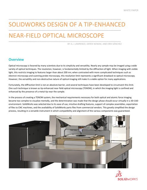
WHITE PAPER.........................................................................................................................................................................................SOLIDWORKS DESIGN OF A TIP-ENHANCED.........................................................................................................................................................................................NEAR-FIELD OPTICAL MICROSCOPE.........................................................................................................................................................................................BY A.J. LAWRENCE, DEREK NOWAK, AND ERIK SÁNCHEZOverviewOptical microscopy is favored by many scientists due to its simplicity and versatility. Nearly any sample may be imaged using a widevariety <strong>of</strong> optical techniques. <strong>The</strong> resolution, however, is fundamentally limited by the diffraction <strong>of</strong> light. When imaging with visiblelight, this restricts imaging to features larger than about 200 nm; when contrasted with more complicated techniques such aselectron microscopy and scanning probe microscopy, this resolution limit represents a significant drawback to optical microscopy.However, the versatility and non-destructive nature <strong>of</strong> optical imaging still make it a viable option for many applications.Fortunately, the diffraction limit is not an absolute barrier, and several techniques have been developed to circumvent this limit.One such technique is known as tip-enhanced near-field optical microscopy (<strong>TENOM</strong>), in which the imaging light is confined andenhanced by the presence <strong>of</strong> a metal tip near the sample.In the process <strong>of</strong> creating a <strong>TENOM</strong> system, the mechanical requirements necessary for both optical and atomic force imagingbecame too complex to visualize mentally, and the determination was made that the design phase should occur virtually in a 3D CADenvironment. <strong>SolidWorks</strong> was selected due to its ease <strong>of</strong> use, intuitive drafting features, support <strong>of</strong> complex assemblies, exportation<strong>of</strong> files to CNC machines, and the availability <strong>of</strong> <strong>SolidWorks</strong> parts files from commercial vendors. This greatly simplified the designprocess, resulting in a versatile instrument in which compatibility and alignment <strong>of</strong> the various components was guaranteed.
1. Beating the diffraction limit <strong>of</strong> optical microscopyOptical microscopy is fundamentally limited by diffraction. When a lens is used to focuslight, the size <strong>of</strong> the focused spot corresponds to the maximum obtainable resolution.Its value is given by 1dλ2 sin= ,( n α )where λ is the wavelength <strong>of</strong> the light, n is the refractive index (a measure <strong>of</strong> the effect<strong>of</strong> the lens material on the speed <strong>of</strong> light), and α is the half-angle <strong>of</strong> the cone <strong>of</strong> lightthat propagates through the lens.<strong>The</strong> quantity (n sin α) is known as the numerical aperture and generally serves as a goodindicator <strong>of</strong> the resolving power <strong>of</strong> a lens. Typical values <strong>of</strong> numerical aperture forobjective lenses range from 0.1 to 1.4, corresponding to a maximum resolution <strong>of</strong> ≈λ/2,or roughly 250 nm, in optical microscopy....................................................<strong>The</strong> diffraction <strong>of</strong> light limitsresolution in optical microscopyto roughly λ/2.In 1928, a technique was proposed 2 to beat the diffraction limit by point scanningthrough a sufficiently small aperture such that light would not propagate. Within onewavelength <strong>of</strong> the source, there exists an evanescent (that is, stagnant) field, the socalled“near-field”, which is non-propagating and thus not subject to diffraction.This technique remained experimentally impossible until the invention <strong>of</strong> atomic forcemicroscopy (AFM) 3 . Replacement <strong>of</strong> the AFM probe tip with a tapered optical fiber 4,5resulted in a resolution <strong>of</strong> 25 nm, or ≈λ/20. This technique is known as near-fieldscanning optical microscopy (NSOM).In 1985, a technique was proposed 6 to further improve resolution while simultaneouslyeliminating the need for an aperture probe. By illuminating a sharp metallic tip with anexternal laser, an enhanced field is generated at the end <strong>of</strong> the probe. As the tip scansthe sample surface, the enhanced field generates a spectroscopic response from thesample. This technique is known as tip-enhanced near-field optical microscopy (<strong>TENOM</strong>)and has shown spatial resolution on the order <strong>of</strong> 20 nm 7 ....................................................Resolution in near-fieldtechniques is limited only by thegeometry <strong>of</strong> the probe.Conceptual drawing <strong>of</strong> <strong>TENOM</strong> probe. “A” is the diffraction limited illumination sourceand “a” is the effective imaging probe 8 .<strong>SolidWorks</strong> <strong>Design</strong> <strong>of</strong> a Tip-Enhanced Near-Field Optical Microscope 2
2. MotivationThis design was originally conceived as a replacement for a heavily modified commercialmicroscope being converted into a <strong>TENOM</strong> system. As the project continued to progressand further modification became necessary, it grew increasingly apparent thatadaptation <strong>of</strong> an existing system would not afford the necessary flexibility. It wastherefore decided to design a system from the ground up with an emphasis on stability,simplicity, and versatility.It soon became apparent that, despite the intended simplicity, it would be nearlyimpossible to mentally visualize each <strong>of</strong> the various components <strong>of</strong> such a complexinstrument and have any confidence in their placement, compatibility, or alignment. Asan alternative, it was decided that the microscope should be constructed in a virtualenvironment using <strong>SolidWorks</strong>. Each individual component was drafted and thenbrought together into one comprehensive assembly, providing a fast and free designphase in which all <strong>of</strong> the parts were guaranteed to fit together exactly as they wereintended to....................................................<strong>The</strong> design phase wasundertaken entirely in a virtual3D CAD environment using<strong>SolidWorks</strong>.3. <strong>Design</strong> <strong>of</strong> optical microscope<strong>The</strong> critical components <strong>of</strong> an optical microscope are the illumination source, thecondenser lens which focuses the illumination light, the objective lens which magnifiesthe image, and the detector. In near-field microscopy, the most practical arrangement isan inverted microscope with epi-illumination, allowing the objective lens to double asthe condenser. <strong>The</strong> physical design <strong>of</strong> the optical microscope provides the opticalpathways necessary for excitation and collection in this system, emulating the function<strong>of</strong> a commercial system at a fraction <strong>of</strong> the price.<strong>The</strong> CAD phase was greatly simplified due to the availability <strong>of</strong> <strong>SolidWorks</strong> parts filesfrom multiple vendors. <strong>The</strong>se files were downloaded and mated with custom parts. <strong>The</strong>first step was construction <strong>of</strong> a stable base. Four 1.5" diameter posts (Thorlabs P8) weremounted to an optical breadboard (Thorlabs MB1824) to support the custom designedbase plate. <strong>The</strong> base plate supports the scan bed, a two axis nanopositioning stage(Physik Instrumente 733.2CL) on which the sample is mounted....................................................<strong>The</strong> part file for the base platewas converted to .dxf format fordirect upload into a CNC mill.3D CAD model <strong>of</strong> optical microscope base plate<strong>The</strong> illumination source, an external laser, is brought into a cube-mounted beam splitter(Thorlabs CM1-BS013) by a periscope consisting <strong>of</strong> two kinematic mirror mounts(Thorlabs KM100) attached to single axis translation stages (Melles Griot 148-103)mounted to the optical breadboard and the bottom <strong>of</strong> the base plate.<strong>SolidWorks</strong> <strong>Design</strong> <strong>of</strong> a Tip-Enhanced Near-Field Optical Microscope 3
<strong>The</strong> beam splitter reflects the light to the objective lens (Olympus 1.4 NA, 60x), which ismounted in a z translation stage (Thorlabs SM1Z). This translator controls the distancebetween the objective and the sample, providing focusing capabilities. <strong>The</strong> light isreflected back down through the objective and beam splitter to a 90° kinematic mirrormount (Thorlabs KCB1), which redirects the light to the detector (Thorlabs APD110A).Two-dimensional cross section view <strong>of</strong> optical pathways in inverted optical microscopedesign. a) Objective lens b) X-Y scanner c) Base plate d) Periscope assemblye) Beam splitter f) Avalanche photodiode<strong>The</strong> implementation <strong>of</strong> point-scanning capabilities allows imaging <strong>of</strong> a much larger areaat increased resolution by measuring the light intensity at each pixel. <strong>The</strong> algorithmsnecessary for scanning and collection are written in LabVIEW and controlled through aNational Instruments data acquisition (DAQ) card (PCIe-7852R) with a fieldprogrammable gate array (FPGA) microprocessor.Fluorescence image <strong>of</strong> bovine pulmonary artery endothelial (BPAE) cells 8<strong>SolidWorks</strong> <strong>Design</strong> <strong>of</strong> a Tip-Enhanced Near-Field Optical Microscope 4
4. Atomic Force Microscopy<strong>The</strong> optical microscope was designed with forethought given to the necessity <strong>of</strong>integration <strong>of</strong> AFM capabilities. <strong>The</strong> custom base plate, which serves as the ceiling andsample holder <strong>of</strong> the optical microscope, functions as the base <strong>of</strong> the AFM, leaving thetwo systems integrated yet independent. A pocket milled into the base plateaccommodates the x-y piezo scan stage....................................................In some cases, parts had to bereverse engineered from twodimensionaldrawings providedby the manufacturer. This wasthe case with the lead screw.3D CAD model <strong>of</strong> AFM backplaneMounted on the base plate is a stable backplane assembly, consisting <strong>of</strong> a thick plateand three braces, all custom designed in <strong>SolidWorks</strong> and machined from cast iron. <strong>The</strong>sole function <strong>of</strong> the backplane assembly is to position the AFM scan head such that thetip is suspended over the sample surface. Mounted to the back <strong>of</strong> the scan head is adovetail (Thorlabs XT66D3) which nests in custom rails mounted to a 50 mm translationstage (Thorlabs LNR50M with drive removed). <strong>The</strong> translation stage is mounted to thebackplane, and the z height is controlled by a stepper motor (Oriental MotorsPK243B1A-SG36) and lead screw (Universal Thread) assembly.<strong>SolidWorks</strong> <strong>Design</strong> <strong>of</strong> a Tip-Enhanced Near-Field Optical Microscope 5
Engineering drawing <strong>of</strong> scan head shell<strong>The</strong> primary design complication <strong>of</strong> the backplane was the three-dimensionalpositioning <strong>of</strong> the AFM tip. <strong>The</strong> x and y dimensions were constrained by the necessityfor the tip, and therefore the center <strong>of</strong> the scan head, to be perfectly centered over theobjective lens, thereby making simultaneous optical and AFM imaging possible. <strong>The</strong> zdimension was less critical due to the inherent flexibility afforded by the 50 mmtranslation stage, but in general, it was desirable that the tip be near the surface whenthe stage was positioned midway through its range <strong>of</strong> travel.Mates between subassemblies ensured compatibility and alignment <strong>of</strong> components.<strong>The</strong> realization <strong>of</strong> these requirements was greatly simplified by the CAD design processundertaken in <strong>SolidWorks</strong>. Separate subassemblies were constructed for the scan head,backplane, and optical microscope. By making the necessary mates within the assembly,such as constraining the dovetail to the dovetail rails, the bottom <strong>of</strong> the backplane tothe top surface <strong>of</strong> the base plate, etc., all but three degrees <strong>of</strong> freedom were<strong>SolidWorks</strong> <strong>Design</strong> <strong>of</strong> a Tip-Enhanced Near-Field Optical Microscope 6
eliminated---the x and y positions <strong>of</strong> the backplane and the z position <strong>of</strong> the scan head.<strong>The</strong> subassemblies were then moved to appropriate locations, revealing the optimalpositions for the mounting holes. For added flexibility, slots were machined in thebackplane braces, allowing 1/4" <strong>of</strong> travel in the y position <strong>of</strong> the backplane.3D CAD model <strong>of</strong> inverted optical microscope with AFM capabilities<strong>The</strong> custom parts were outlined in <strong>SolidWorks</strong> drawing files and fabricated from castiron, aluminum, and MACOR. Once assembled, the microscope was placed in a lightpro<strong>of</strong> enclosure on a floating optical table to shield it from external fields and vibration.<strong>The</strong> end result is a functional atomic force inverted optical microscope....................................................<strong>The</strong> final design is a highlyadaptable, low-cost instrumentwith potential capabilitiesbeyond those <strong>of</strong> anycommercially available system.Topographic AFM image <strong>of</strong> pits on the surface <strong>of</strong> a DVD 8<strong>SolidWorks</strong> <strong>Design</strong> <strong>of</strong> a Tip-Enhanced Near-Field Optical Microscope 7
5. Tip-Enhanced Near-Field Optical MicroscopyWith the optical and AFM systems functional, integration <strong>of</strong> a specialized probe tip,created via electrochemical etching and focused ion beam milling, added near-fieldimaging capabilities to the system 9,10 .Three images <strong>of</strong> same region <strong>of</strong> interest using different optical systems. a) Near fieldtwo-photon fluorescence image obtained with low cost near-IR diode laser. b) Near fieldtwo-photon fluorescence image obtained with a much more expensive pulsed lasersystem c) Diffraction-limited two-photon fluorescence image.<strong>SolidWorks</strong> proved to be an invaluable tool in the development <strong>of</strong> this instrument.Without the support for complex assemblies and the intuitive mating capabilities thes<strong>of</strong>tware affords, the design phase <strong>of</strong> this project would have proven unnecessarilycomplicated.1 E. Abbe, “A contribution to the theory <strong>of</strong> the microscope and the nature <strong>of</strong> microscopicvision," Archiv fur Mikroskopische Anatomie, 1874.2 E. Synge, “A suggested method for extending the microscopic resolution into theultramicroscopic region,” Phil. Mag., vol. 6, no. 356, 1928.3 G. Binnig, C. F. Quate, and C. Gerber, “Atomic force microscope," Phys. Rev. Lett., vol.56, pp. 930-933, Mar. 1986.4 A. Lewis, M. Isaacson, A. Harootunian, and A. Muray, “Development <strong>of</strong> a 500 Å spatialresolution light microscope,” Ultramicroscopy, vol. 13, no. 3, pp. 227- 231, 1984.<strong>SolidWorks</strong> <strong>Design</strong> <strong>of</strong> a Tip-Enhanced Near-Field Optical Microscope 8
5 D. W. Pohl, W. Denk, and M. Lanz, “Optical stethoscopy: Image recording with resolution λ/20,"Applied Physics Letters, vol. 44, pp. 651-653, Apr. 1984.6 J. Wessel, "Surface-enhanced optical microscopy," J. Opt. Soc. Am. B 2, 1538-1541, 1985.7 E. J. Sánchez, L. Novotny, and X. S. Xie, “Near-Field Fluorescence Microscopy Based on Two-Photon Excitation with Metal Tips,” Phys. Rev. Lett., vol. 82, pp. 4014-4017, May 1999.8 D. B. Nowak, A. J. Lawrence, and E. J. Sánchez, "A low cost non-linear fluorescence near-field/farfieldmicroscope," Nanotechnology (IEEE-NANO), 2011 11th IEEE Conference on , vol., no., pp.576-581, 15-18 Aug 2011.9 D. B. Nowak, A. J. Lawrence, and E. J. Sánchez, “Apertureless near-field/far-field cw two-photonmicroscope for biological and material imaging and spectroscopic applications," Appl. Opt., vol.49, pp. 6766-6771, Dec 2010.10 D. B. Nowak, A. J. Lawrence, Z. K. Dzegede, J. C. Hiester, C. Kim, and E. J. Sánchez, “Fieldprogrammable gate array based reconfigurable scanning probe/optical microscope," Rev. Sci.Instrum., vol. 82, p. 103701, Oct 2011.......................................................................................................................This project is being disseminated an as open system design. For moreinformation and relevant documentation, please visit the ANSOM Projectwebpage at ansom.research.pdx.edu.......................................................................................................................……………………………………………………………………………………………………………………………………………………………………………………………………………………Dassault Systèmes<strong>SolidWorks</strong> Corp.300 Baker AvenueConcord, MA 01742 USAPhone: 1 800 693 9000Outside the US: +1 978 371 5011Email: info@solidworks.comwww.solidworks.com<strong>SolidWorks</strong> is a registered trademark <strong>of</strong> Dassault Systèmes <strong>SolidWorks</strong> Corp. All other company and product names are trademarksor registered trademarks <strong>of</strong> their respective owners. ©2010 Dassault Systèmes. All rights reserved. MKCADWPENG1210