PDF of Aug. Issue - IEEE Photonics Society
PDF of Aug. Issue - IEEE Photonics Society
PDF of Aug. Issue - IEEE Photonics Society
- No tags were found...

Create successful ePaper yourself
Turn your PDF publications into a flip-book with our unique Google optimized e-Paper software.
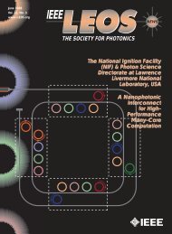
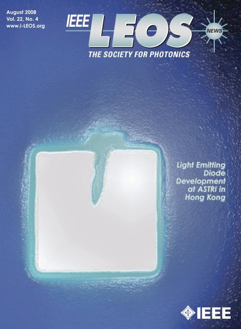
<strong>Aug</strong>ust 2008Vol. 22, No. 4www.i-LEOS.org<strong>IEEE</strong>NEWSTHE SOCIETY FOR PHOTONICSLight EmittingDiodeDevelopmentat ASTRI inHong Kong
President’sColumnJohn H. MarshIn previous columns I have described new activities in membershipand in conferences. This month I will focus on exciting developmentsin publications, which involve cross society collaboration,coverage <strong>of</strong> more application areas and a major move toon-line publication. These developments, moreover, have grownout <strong>of</strong> the long range strategic plan.When the LEOS Board <strong>of</strong> Governors met during CLEO inMay, it approved two new journals. I am delighted to report thatboth these proposals have passed all the necessary approvalstages within <strong>IEEE</strong> and will be launched next year.Journal <strong>of</strong> Optical Communicationsand NetworkingThe <strong>IEEE</strong>/OSA Journal <strong>of</strong> Optical Communications and Networking(JOCN) will cover advances in state-<strong>of</strong>-the-art optical communicationsand networks. In doing so, it will complement the Journal<strong>of</strong> Lightwave Technology, which is oriented towards device andhardware implementation. The new JOCN will replace both theexisting OSA Journal <strong>of</strong> Optical Networking and the Optical Communicationsand Networking Series published three times a year asPart II <strong>of</strong> the <strong>IEEE</strong> Journal on Selected Areas in Communications.The JOCN will therefore <strong>of</strong>fer comprehensive coverage <strong>of</strong> theoreticaland practical aspects <strong>of</strong> optical communication systemsand networks in one journal.The JOCN will be available on-line and in a printed version,with rapid posting <strong>of</strong> accepted papers. This initiative not onlybuilds the strong collaboration between LEOS, the <strong>IEEE</strong>Communications <strong>Society</strong> and OSA, but also replaces what areeffectively two journals with a single one.<strong>IEEE</strong> <strong>Photonics</strong> JournalThe <strong>IEEE</strong> <strong>Photonics</strong> Journal is a particularly important and excitingdevelopment for LEOS. The <strong>Photonics</strong> Journal will onlybe published on-line, and therefore represents a significant departurenot only for LEOS but also for the <strong>IEEE</strong> as a whole.Its scope is intended to include areas where LEOS membersare active, but which have not always been well represented inLEOS publications, and new interdisciplinary areas. The scopeincludes:• Fiber optics and optical communications devices, systems,and technologies• Photovoltaics• Micro Opto Electro Mechanical Systems (MOEMS)• Microwave photonics• Optical sensorsAlthough LEOS will have sole responsibility for publishing the<strong>Photonics</strong> Journal, the involvement <strong>of</strong> other societies is importantin building its interdisciplinary aspect. Three other <strong>IEEE</strong> societieshave already become technical co-sponsors:• <strong>IEEE</strong> Engineering in Medicine and Biology <strong>Society</strong>• <strong>IEEE</strong> Nanotechnology Council (subject to approval by theirCouncil)• <strong>IEEE</strong> Consumer Electronics <strong>Society</strong>Motivation and StrategyThe motivation behind both journals, but particularly the<strong>Photonics</strong> Journal, reflects the strategic priorities <strong>of</strong> the LEOSRetaininghooks tohold coildown(continued on page 27)63mm, 101mm and304mm Spool DiametersFiber Coil Stack PacksPress-fitprotectionforconnectors• Photon sources from far infrared to x-rays• Photonic materials and engineered photonic structures• Integrated optics and optoelectronics• Ultrafast, attosecond, high field and short wavelengthphotonics• Biophotonics including DNA photonics• Nanophotonics• Magnetophotonics• Fundamentals <strong>of</strong> light propagation and interaction;nonlinear effects• Optical data storage<strong>Aug</strong>ust 2008 <strong>IEEE</strong> LEOS NEWSLETTER 3
Research Highlights:Light Emitting Diode Developmentat ASTRI in Hong KongShu Yuan, Chen Jung Tsai, Ming Lu, Benson Liaw, and Enboa Wu*LED Program, Material and Packaging Technologies GroupHong Kong Applied Science and Technology Research Institute, Hong KongDr. Enboa Wu, Vice President and Group Director,e-mail: enboa@astri.orgThe Applied Science and Technology Research Institute (AS-TRI) in Hong Kong has been working on advanced technologiesin most segments <strong>of</strong> the LED technology chain: chip design andfabrication, packaging, and applications on display systems andgeneral lighting, through three divisions, namely Display SystemDivision, General Lighting Division, and LED Devices Division.Core LED technologies in ASTRI include: high dynamic rangeLCD display, large-sized thin LED backlight with local dimming,embedded and companion pico-projectors, and sapphire substrateremoval by modified chemical mechanical polishing (CMP)method for power GaN LED chips. In this article we first providean overview <strong>of</strong> some <strong>of</strong> the technologies developed at ASTRI forDisplay Systems and LEDs for backlighting and general lightingbefore discussing some <strong>of</strong> the core device technologies.Display System TechnologiesOur focus on LED applications in displays includes thefollowing areasFigure 1. 47” LCD TV with 2-D local dimming using RGB LEDsfor backlightInput ImageGraylevel Dimming RGB Dimming Adaptive Dimming1. High Dynamic Range Display SystemBy combining LED backlight with the two dimensional (2-D)local dimming image processing technology, we have establisheda technology platform for high dynamic range display systems.This platform includes LED backlight with 2-D local dimmingalgorithms, video image dynamic range expansion, adaptive colormanagement, and backlight power saving management. For localdimming, we are able to integrate gray level dimming with RGBcolor dimming to come up with a method designated as adaptiveRGB dimming. The developed HDR technology also allowsenhancement <strong>of</strong> color depth from 8 bits to higher than 10 bits,which is considered essential for HD TVs. Figure 1 and Figure2 show ASTRI prototypes with features <strong>of</strong> high brightness (500-1500 nits), high dynamic contrast (>100,000:1), power saving(30-50%), and high color gamut (>110% NTSC).Figure 2. Different 2-D dimming algorithms for LED backlights.Upper image: input image, lower images: LED Backlight imagesFigure 3. ASTRI’s 32” light strip LED backlight solution: (Left) Power LEDs to the lightguide; (Middle) Light guides for backlight; (Right) Assembled backlight.2. Novel Thin LED backlight unitfor LCD TVThrough novel second optical designs, wehave developed various thin (15-25mm)LED backlight solutions (direct emitting &side emitting types) for LCD TVs with localdimming function. This results in improvedbrightness and uniformity, along with possibilitiesto utilize fewer high power LEDsor mid-level power LEDs, at lower cost andpower consumption. A typical example is theuse <strong>of</strong> the novel light guide strip with only48 high power (2W) LEDs to construct a 32”LED backlight, it keeps the backlight thinnerthan 20 mm, as shown in Figure 3.4 <strong>IEEE</strong> LEOS NEWSLETTER <strong>Aug</strong>ust 2008
Accelerating the pace <strong>of</strong> engineering and scienceOver one million people around theworld speak MATLAB.Engineers and scientists in every fieldfrom aerospace and semiconductorsto biotech, financial services, andearth and ocean sciences use it toexpress their ideas.Do you speak MATLAB?Saturn's northern latitudesand the moon Mimas.Image from theCassini-Huygens mission.Related article atmathworks.com/ltc®PHOTO: European Space Agency ©2008 The MathWorks, Inc.The language <strong>of</strong> technical computing<strong>Aug</strong>ust 2008 <strong>IEEE</strong> LEOS NEWSLETTER 5
3. Pico-ProjectorCombining LED light source with micro-display based on liquidcrystal on silicon, ASTRI has developed a compact projection modulewhich can serve as a standalone companion projector (
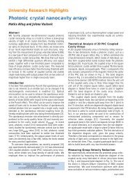
Figure 6 A two-inch wafer with sapphire thinned to about 10 micron (left). Scanning electronmicroscope image <strong>of</strong> an LED mesa after sapphire is removed by modified CMP (middle). Emission<strong>of</strong> light from an LED with sapphire removed when current is applied (right).and color tuning modules for advanced lighting control. By integratingsensor technologies into the RF-based wireless controlledlighting system, a comfortable and energy efficient lighting systemis demonstrated.LED Devices TechnologiesThe LED chip industry has enjoyed a relatively long period <strong>of</strong> prosperity.The next growth segment in LED chip industry is powerLED chips that consume 1W or more electrical power per chip (die).At ASTRI, we have developed designs and processes for makingLEDs using one-dimensional photonic crystals, indium tin oxide(ITO), and removal <strong>of</strong> sapphire by a modified chemical and mechanicalpolishing (CMP) method.One <strong>of</strong> the key technologies for power GaN LED chips is theremoval <strong>of</strong> the sapphire substrate and replacing it with a new substrateto make the so-called “Vertical LEDs”. To extract more lightout <strong>of</strong> the chip, surface texturing is needed. This process can be easilydone on the n-GaN side <strong>of</strong> the chip after the sapphire substrateis removed. For reliable operation <strong>of</strong> the power LED chips, heatgenerated during operation must be removed efficiently and quickly,which can be achieved by bringing the whole surface <strong>of</strong> the p-side<strong>of</strong> the chip into intimate contact with ametal block and remove the originalsapphire substrate. When even higherpower is needed, the area <strong>of</strong> the LEDchip may be increased. All these goalscan be achieved by removing the originalsapphire substrate and replacing itwith a new substrate such as copper orsilicon substrate.The established mainstream method<strong>of</strong> removing sapphire is laser lift<strong>of</strong>f. However, the laser lift<strong>of</strong>fmethod is a proprietary process protected by many different patentsand has some yield issues. Many companies have filed patentsin this area and it is not easy for others to use. The productionyield <strong>of</strong> laser lift<strong>of</strong>f is also relatively low compared with that <strong>of</strong>other standard LED manufacturing methods. To overcome theseproblems, we have developed a novel method for sapphire removal:the modified CMP method for power device applications. Somepreliminary results are shown in Figure 6. The CMP method doesnot have major patent issues. ASTRI is a pioneer in this technologyAs CMP is a more “conventional” method used widely insilicon integrated circuit fabrication, and most GaN LED companiesalready do sapphire thinning by mechanical polishing, thisCMP method is expected to gain wide acceptance when it isapplied to mass production.In conclusion, the LED Program at ASTRI in Hong Kong hasa strong technology platform for the LED industry in Greater Chinaarea. We have developed core technologies in LED display systems,general lighting, and GaN chip design and fabrication. Strongindustry relationships have been established for commercialization<strong>of</strong> these technologies.
8 <strong>IEEE</strong> LEOS NEWSLETTER <strong>Aug</strong>ust 2008
News2008 <strong>IEEE</strong>/LEOS Award WinnersThe <strong>IEEE</strong> Lasers & Electro-Optics <strong>Society</strong> announcedthe winners <strong>of</strong> the Aron Kressel Award and theDistinguished Service Award for 2008. The Awards willbe presented during the Awards Banquet at the LEOSAnnual Meeting:Aron Kressel Award will be presented to HenrykTemkin – “for outstanding contributions and leadership inadvancing opto-electronic materials and devices spanningfrom the infrared to the ultraviolet.”Distinguished Service Award will be presented toJames Coleman – “for contributions to and leadership inthe area <strong>of</strong> publications.”For more information on the awards, check the LEOSweb site (www.i-LEOS.org).2008 LEOS Graduate Student FellowshipWinners AnnouncementThe <strong>IEEE</strong> Lasers & Electro-Optics <strong>Society</strong> announced the winners <strong>of</strong> the LEOS Graduate Student Fellowships for 2008.The Fellowships will be presented during the Awards Banquet at the LEOS Annual Meeting to:Tomohiro Amemiya- The University <strong>of</strong> TokyoRanojoy Bose - Columbia UniversityJia Chen - Technische Universitat MunchenMehdi DaneshPanah - University <strong>of</strong> ConnecticutYoga Divayana - Nanyang Technological UniversityIvana Gasulla - Universidad Politecnica de ValenciaAlireza Hassani - Ecole Polytechnique de MontrealBas Huiszoon - Eindhoven University <strong>of</strong> TechnologyXiankai Sun - California Institute <strong>of</strong> TechnologyPhilippe Tassin - Vrije Universiteit BrusselWithawat Withayachumnankul - The University <strong>of</strong> AdelaideLin Zhang - University <strong>of</strong> Southern CaliforniaThe LEOS Graduate Student Fellowship Program was established to provide Graduate Fellowships to outstanding LEOSstudent members pursuing graduate education within the LEOS field <strong>of</strong> interest.For more information on the program, check the Student site on the LEOS Home Page (www.i-LEOS.org).Call for Nominations:The <strong>IEEE</strong> LEOS Young Investigator AwardThe <strong>IEEE</strong> LEOS Young Investigator Award was establishedto honor an individual who has made outstanding technicalcontributions to photonics (broadly defined) prior to his or her35th birthday.The award shall consist <strong>of</strong> a certificate <strong>of</strong> recognitionand an honorarium <strong>of</strong> $1,000. The funding for this awardis being sponsored by General <strong>Photonics</strong> Corporation.Nomination packages will be due at the LEOSExecutive Office by 30 September. Nominees must beunder 35 years <strong>of</strong> age on Sept. 30th <strong>of</strong> the year in whichthe nomination is made. The award may be presentedeither at the Optical Fiber Communications Conference(OFC), or the Conference on Lasers and Electro-Optics(CLEO), to be selected by the recipient.Nomination packages consist <strong>of</strong> a nomination cover page,a statement <strong>of</strong> the nominee’s research achievements in photonics,the nominee’s curriculum vitae, and three to fivereference letters (to be received at the LEOS <strong>of</strong>fice prior tothe deadline).Please consider nominating an under-age-35 colleaguefor the inaugural cycle <strong>of</strong> this award!For full information about the LEOS awards programlook under the “Awards” tab on the LEOS web site (http://www.i-leos.org/)Nomination form can be found on page 11.10 <strong>IEEE</strong> LEOS NEWSLETTER <strong>Aug</strong>ust 2008
News (cont’d)<strong>Aug</strong>ust 2008 <strong>IEEE</strong> LEOS NEWSLETTER 11
News (cont’d)LEOS Candidates for 2009-2011Board <strong>of</strong> GovernorsBallots for the election <strong>of</strong> candidates to the Board <strong>of</strong> Governors will be mailed soon to all voting members. This year’s candidates are:Jose CapmanyUniversity Politecnica de ValenciaS.-L. ChuangUniversity <strong>of</strong> IllinoisJeffrey KashIBM ResearchFumio KoyamaTokyo Institute <strong>of</strong> TechnologyEl-Hang LeeInha UniversityMichal LipsonCornell UniversityJohn O’BrienUniversity <strong>of</strong> Southern CaliforniaIan WhiteUniversity <strong>of</strong> CambridgePresident’s Column(continued from page 3)Board <strong>of</strong> Governors. Under the leadership <strong>of</strong> Carmen Menoni, ourVice President for Publications, and her predecessor Jim Coleman,LEOS has developed a robust plan for taking publications into newtopic areas and towards on-line publication. This requires a longterm vision, as practical and commercial considerations preventrapid implementation. LEOS is an integral part <strong>of</strong> <strong>IEEE</strong> and LEOSpublications are firstly and foremost <strong>IEEE</strong> journals. The LEOSjournals are among the highest rated <strong>IEEE</strong> publications, and boththe <strong>Society</strong> and the Institute will rightly only introduce changeafter a robust process <strong>of</strong> review.A fundamental aspect <strong>of</strong> the plan is that all LEOS Journalsshould be completely electronic by a fixed future date. However,<strong>IEEE</strong> has no on-line only journals, so it is not currently possibleto fix such a date. The <strong>Photonics</strong> Journal represents a first steptowards full electronic publication for the entire Institute.A second aspect <strong>of</strong> the plan is to serve LEOS members andthe LEOS community. The <strong>Photonics</strong> Journal will report researchin emerging and interdisciplinary areas <strong>of</strong> photonics science andtechnology spanning the wide spectrum <strong>of</strong> topics embraced byLEOS and represented by its Technical Committees. Authorsare, moreover, increasingly demanding short times to publicationfor reporting top quality research; however, rapid publicationis <strong>of</strong>ten accompanied by a drop in the written quality andintelligibility <strong>of</strong> the papers. The <strong>Photonics</strong> Journal will combinerapid publication with a process <strong>of</strong> ‘light copy editing’ to ensurehigh written quality.A final aspect <strong>of</strong> the plan is to <strong>of</strong>fer open access. Open accessis advancing rapidly for dissemination <strong>of</strong> research results, but itplaces the entire cost associated with publication on the author.This cost may inhibit publication or lead authors to choose ajournal where the bulk <strong>of</strong> the costs fall on the readers, as is thecase for most conventional journals. The <strong>Photonics</strong> Journal will<strong>of</strong>fer a ‘hybrid’ model where authors can choose whether or notto pay a fee for open access. All papers will be accessible throughXplore and will be displayed in single column style appropriateto viewing on a screen. In the future it will be possible toinclude figures and photographs that can be enlarged, text thatcan be highlighted, multimedia such as video and podcasts, and<strong>of</strong>fer active links to references and other papers.I would like to congratulate Carmen for her vision in definingthe scope and nature <strong>of</strong> this new journal. I would also congratulateher for piloting both proposals through LEOS and<strong>IEEE</strong>, a process which requires approval from numerous committees.Because the Journal is so fundamentally different fromother <strong>IEEE</strong> publications it also required approval from the highestcommittee concerned with publications, the <strong>IEEE</strong> PublicationServices and Products Board. The journal will also present newchallenges to Linda Matarazzo and her team in the LEOS publicationsgroup.It is also a key part <strong>of</strong> the LEOS strategic plan to work withother societies, within and outwith <strong>IEEE</strong>. I am personallydelighted that these initiatives have already brought increasedcollaboration with five different societies.So next year we will be launching these two publications –the <strong>IEEE</strong> <strong>Photonics</strong> Journal and the <strong>IEEE</strong>/OSA Journal <strong>of</strong> OpticalCommunications and Networking. Both journals are exciting developmentsfor LEOS, and I am confident they will meet importantneeds <strong>of</strong> our members and the wider LEOS community.12 <strong>IEEE</strong> LEOS NEWSLETTER <strong>Aug</strong>ust 2008
Career Section<strong>IEEE</strong>/LEOS William Streifer ScientificAchievement Award Recipient: Fumio KoyamaThe <strong>IEEE</strong>/LEOS William Streifer ScientificAchievement Award is given torecognize an exceptional single scientificcontribution, which has had a significantimpact in the field <strong>of</strong> lasers andelectro-optics in the past 10 years. Theaward is given for a relatively recent,Fumio Koyama single contribution, which has had amajor impact on the LEOS researchcommunity. It may be given to an individual or a group fora single contribution <strong>of</strong> significant work in the field.Fumio Koyama received a B.S., M.S., and Ph.D. degrees inPhysical Electronics from the Tokyo Institute <strong>of</strong> Technology,Tokyo, Japan, in 1980, 1982 and 1985, respectively. He is aPr<strong>of</strong>essor <strong>of</strong> Microsystem Research Center, P&I Lab., TokyoInstitute <strong>of</strong> Technology. Currently, he is doing research onVCSELs, photonic integrated devices, optical MEMS devices,and related semiconductor micr<strong>of</strong>abrication technologies.From 1992 to 1993 he was with AT&T Bell Labs. CrawfordHill as a visiting researcher. For more than 20 years, FumioKoyama has contributed to VCSEL photonics and singlemodelasers for broadband optical communications. In 1985,he joined the research team <strong>of</strong> Pr<strong>of</strong>. Emeritus Kenichi Iga<strong>of</strong> Tokyo Institute <strong>of</strong> Technology, who is the inventor <strong>of</strong>VCSELs. He realized the first room temperature CW operations<strong>of</strong> VCSELs in 1988. He and his co-workers have spentmuch effort and did contributions for the progress <strong>of</strong> VCSELphotonics. He also contributed to the suggestion and understandingfor frequency chirping in external modulators. Thisconcept is important for long-haul and broadband opticalcommunication networks with avoiding frequency chirping.He received the <strong>IEEE</strong> Student Paper Award in 1985 and waselected a Fellow <strong>of</strong> the <strong>IEEE</strong> in 2008.<strong>IEEE</strong>/LEOS Engineering AchievementAward Recipient: Kent D. ChoquetteThe <strong>IEEE</strong>/LEOS Engineering AchievementAward is given to recognize anexceptional engineering contributionthat has had a significant impact on thedevelopment <strong>of</strong> lasers or electro-opticstechnology or the commercial application<strong>of</strong> technology within the past 10Kent D. Choquette years. It may be given to an individualor a group for a single contribution <strong>of</strong>significant work in the field. The intention is to recognizesome significant engineering contribution which has resultedin development <strong>of</strong> a new component, a new processingtechnique, or a new engineering concept which has hada significant impact in either bringing a new technologyto the market, significantly improving the manufacturability<strong>of</strong> a component or device, or creating a new technologywhich will greatly accelerate or stimulate R&D.Kent D. Choquette received a B.S. degrees in EngineeringPhysics and Applied Mathematics from the University<strong>of</strong> Colorado-Boulder in 1984 and the M.S. andPh.D. degrees in Materials Science from the University<strong>of</strong> Wisconsin-Madison in 1985 and 1990, respectively.From 1990 to 1992 he held a postdoctoral appointment atAT&T Bell Laboratories, Murray Hill, NJ. He then joinedSandia National Laboratories in Albuquerque, NM, andfrom 1993 to 2000 was a Principal Member <strong>of</strong> TechnicalStaff. He became a Pr<strong>of</strong>essor in the Electrical and ComputerEngineering Department at the University <strong>of</strong> Illinoisat Urbana-Champaign in 2000. His Photonic DeviceResearch Group is centered around the design, fabrication,characterization, and applications <strong>of</strong> vertical cavitysurface-emitting lasers (VCSELs), photonic crystal lightsources, nan<strong>of</strong>abrication technologies, and hybrid integrationtechniques for photonic devices. He has authoredmore than 200 technical publications and three bookchapters, and has presented numerous invited talks andtutorials. From 2000 to 2002, he was an <strong>IEEE</strong>/Lasers andElectro-Optics <strong>Society</strong> (LEOS) Distinguished Lecturer.Pr<strong>of</strong>. Choquette has served as an Associate Editor <strong>of</strong> the<strong>IEEE</strong> Journal <strong>of</strong> Quantum Electronics and <strong>IEEE</strong> PhotonicTechnology Letters, and as a Guest Editor <strong>of</strong> <strong>IEEE</strong> Journal<strong>of</strong> Selected Topics in Quantum Electronics. He is a Fellow<strong>of</strong> the <strong>IEEE</strong>, a Fellow <strong>of</strong> the Optical <strong>Society</strong> <strong>of</strong> America,and a Fellow <strong>of</strong> SPIE. Kent and his wife Lori live in UrbanaIllinois, and have three teenage daughters, Amber,Kelsey, and Nicole. The Choquette family enjoys skiing,backpacking, sports, and gardening.<strong>Aug</strong>ust 2008 <strong>IEEE</strong> LEOS NEWSLETTER 13
Career Section (cont’d)2008 <strong>IEEE</strong> Eric E. Sumner Award Recipient:Thomas L. KochThe <strong>IEEE</strong> Eric E. Sumner Award wasestablished by the <strong>IEEE</strong> Board <strong>of</strong> Directorsin 1995. It may be presentedannually, to an individual or a team <strong>of</strong>not more than three, for outstandingcontributions to communications technology.Recipient selection is administeredby the Awards Board through itsThomas L. KochTechnical Field Awards Council. It isnamed in honor <strong>of</strong> Eric E. Sumner, 1991 <strong>IEEE</strong> President,who retired as Vice President, Operations Planning, AT&TBell Laboratories after a long and distinguished career.Thomas L. Koch’s work in the area <strong>of</strong> photonics has led toimproved optical fiber communication links that form thebackbone <strong>of</strong> today’s Internet and Telecommunications Networks.His broad spectrum <strong>of</strong> contributions extend fromthe design and demonstration <strong>of</strong> new concepts in semiconductorlasers to providing new approaches to modeling optoelectronicdevices and their impact on fiber communicationsystem performance. Koch’s role in the development <strong>of</strong>photonic integrated circuits, which are single microchipscontaining many microscopic photonic components, enabledthe incorporation <strong>of</strong> highly sophisticated functions atlower cost and higher reliability. An <strong>IEEE</strong> Fellow, he holds35 patents and has authored or co-authored over 300 journaland conference publications and co-edited the two-volumebook “Optical Fiber Telecommunications III” with Ivan. P.Kaminow. Dr. Koch has previously received the WilliamStreifer Award for Scientific Achievement from <strong>IEEE</strong> LEOSand is a member <strong>of</strong> the National Academy <strong>of</strong> Engineering.He holds a Bachelor’s in Physics from Princeton University,N.J., and a Doctorate in Applied Physics from CaliforniaInstitute <strong>of</strong> Technology in Pasadena.Membership SectionNanotech: Driver <strong>of</strong> Electronics, <strong>Photonics</strong>,Energy, and Bio-MedFourth Annual Symposium <strong>of</strong> the <strong>IEEE</strong> San Francisco Bay AreaNanotechnology CouncilCo-sponsored by the Santa Clara Valley chapters <strong>of</strong> <strong>IEEE</strong> LEOS,CPMT, and EDS <strong>IEEE</strong> LEOS NewsletterBrent K. WhitlockTreasurer and Past Chair, Santa Clara Valley chapter <strong>of</strong> <strong>IEEE</strong> LEOS,June 24, 2008On Tuesday May 20, 2008, the <strong>IEEE</strong> San Francisco Bay AreaNanotechnology Council’s Fourth Annual Symposium on“Nanotech: Driver <strong>of</strong> Electronics, <strong>Photonics</strong>, Energy, and Bio-Med” was held. The Santa Clara Valley chapter <strong>of</strong> the <strong>IEEE</strong>Lasers and Electro-Optics <strong>Society</strong> (LEOS) co-sponsored thesymposium, along with the Santa Clara Valley chapters <strong>of</strong> the<strong>IEEE</strong> Components, Packaging, and Manufacturing Technology<strong>Society</strong> (CPMT) and the <strong>IEEE</strong> Electron Devices <strong>Society</strong>(EDS). One hundred fifteen people attended the symposiumheld at National Semiconductor Corporation’s ConferenceCenter in Santa Clara, California. The full day symposiumbrought together leading experts in research and industry todiscuss business and technology trends in nanotechnology.<strong>Photonics</strong> was a pervasive topic in the NanotechnologySymposium this year. The symposium featured a keynotespeaker, a luncheon speaker, four sessions <strong>of</strong> invited papers,and a panel discussion entitled “Nanotechnology: Show Methe Money.” In all, there were 13 technical talks and three14 <strong>IEEE</strong> LEOS NEWSLETTER <strong>Aug</strong>ust 2008
Membership Section (cont’d)panelists in the panel discussion, in addition to the sessionchairs and panel session moderator. Further details about theevent can be found in the archive <strong>of</strong> past events at the <strong>IEEE</strong>SFBA Nanotechnology Council web site at http://www.ieee.org/nano.The program began with the keynote presentation by Dr.Paolo Gargini, an Intel Fellow, Technology and ManufacturingGroup, and Director <strong>of</strong> Technology Strategy at Intel Corporation.Dr. Gargini was elevated to <strong>IEEE</strong> Fellow in 2008. Dr. Garginispoke about nanotechnology opportunities and challenges forthe next decade. Dr. Gargini began his talk by tracing thedevelopment <strong>of</strong> the IC and CMOS technologies starting withThomas Edison through to today. Dr. Gargini stressed howlong it takes for a technology to advance from science incubationthrough to maturity. In his view, nanotechnology will playan increasingly important role in electronics to compensate forthe inability to continue to scale oxide dimensions at the 65 nmtechnology node and beyond. Dr. Gargini also spoke <strong>of</strong> carbonnanotubes, carbon nanoribbons, and spintronics as importanttechnologies for the future. The challenge is to generate another50 years <strong>of</strong> technological growth.The luncheon presentation was given by Pr<strong>of</strong>essor EliYablonovitch <strong>of</strong> the Electrical Engineering andComputer Sciences Department at theUniversity <strong>of</strong> California, Berkeley. Pr<strong>of</strong>essorYablonovitch discussed nanophotonic siliconcircuits as a commercial technology, usingLuxtera as a case study. Silicon technology canprovide many <strong>of</strong> the requirements for nanophotonicintegration, including many <strong>of</strong> the commonoptoelectronic components. Pr<strong>of</strong>.Yablonovitch pointed out that all the customarilyrequired optoelectronic components areavailable now in silicon. While silicon lasersources are not available, continuous wave opticalpower can be provided from <strong>of</strong>f-chip, just asdc power is currently provided from <strong>of</strong>f-chip.The first commercial applications <strong>of</strong> CMOSphotonics are in the form <strong>of</strong> “Optical ActiveCable,” optical cables with electrical plugs atthe ends. For example, a 40Gb/s cable for largedata-centers was recently demonstrated at theSuperComputer show.The four sessions were on the topics <strong>of</strong>Nanodevice Materials and Processes Below 32nm, <strong>Photonics</strong>, Alternative Energy and Storage,and Nano and Bio Sensors. In addition to the<strong>Photonics</strong> session, several <strong>of</strong> the other sessionsincluded some discussions <strong>of</strong> optical and photonicstechnologies, from optical lithography tophotovoltaics to optical interconnects. Opticallithography continues to be an important technology for semiconductormanufacturing. However, while the feature sizesdecrease, new techniques and technologies are needed to supplementoptical lithography to keep pace. Ken Rygler <strong>of</strong> MolecularImprints discussed imprint patterning technologies, while Dr.Kimon Michaels <strong>of</strong> <strong>PDF</strong> Solutions discussed design for manufacturability(DFM) including more complex modeling <strong>of</strong> layoutvariation performance and simplified optical proximitycorrection (OPC) and design rules. There is quite a bit <strong>of</strong> workgoing on in photovoltaics these days, with the goal <strong>of</strong> increasingefficiency. For example, Dr. Yue Wu <strong>of</strong> the Department <strong>of</strong>Chemistry at the University <strong>of</strong> California, Berkeley discussedsemiconductor nano-crystal based photovoltaics that enablehigh efficiency solar cells. As Pr<strong>of</strong>. Krishna Saraswat <strong>of</strong> theDepartment <strong>of</strong> Electrical Engineering at Stanford Universitypointed out, optical interconnect technology has been demonstrated.However, it remains to be seen whether optical interconnectswill be used on-chip in practice, due to economicconsiderations.In the <strong>Photonics</strong> session, Pr<strong>of</strong>. Cun-Zheng Ning <strong>of</strong>Arizona State University, <strong>IEEE</strong> LEOS Distinguished Lecturer,spoke about semiconductor nanowire based nanophotonics.<strong>Aug</strong>ust 2008 <strong>IEEE</strong> LEOS NEWSLETTER 15
Membership Section (cont’d)Keynote speaker Dr. Paulo Gargini beingpresented with a plaque by organizers Dr.K.R.S. Murthy and Dr. Kris Verma.Luncheon speaker Pr<strong>of</strong>. Eli Yablonovitchbeing thanked by organizer Dr. BrentWhitlockSession organizers and participants (leftto right): Chris Graham, Pallab Chatterjee,Dr. Kris Verma, Dr. KRS Murthy,Barry Epstein, and Rich HelfrichNanowires can be used for photonics including nanolasers,broadly tunable lasers, LEDs, waveguides, and full spectrumsolar cells. Pr<strong>of</strong>. Ning also discussed reducing photonicdevice sizes by using surface plasmonics. Pr<strong>of</strong>. David Atwood<strong>of</strong> the University <strong>of</strong> California, Berkeley and LawrenceBerkeley National Laboratory discussed 3D imaging using20 nm x-ray microscopy. The Advanced Light Source atLawrence Berkeley National Laboratory is used to producesynchrotron radiation for high-resolution zone plate microscopy.Other applications include extreme ultraviolet lithography.Dr. Michael O’Connell, Sr. Scientist at Unidym, spokeabout carbon nanotubes and their many applications includingmaterials, electronics, optoelectronics, medicine, andenergy. The challenge is to make a very transparent filmusing the blackest material known, having conductivitycomparable to metal, and having stability with respect totemperature.In the Panel Session moderated by Pallab Chatterjee,Senior Editor <strong>of</strong> Extension Media, the panelists addressed thetopic <strong>of</strong> “Nanotechnology: Show Me the Money.” RichHelfrich <strong>of</strong> Alameda Capital, founder <strong>of</strong> Vitesse Semiconductor,spoke about we are becoming aware <strong>of</strong> plenty <strong>of</strong> opportunitiesrelated to nanotechnology, but the big issue today is risk.He spoke about what VCs look for when considering investingin a new venture. Barry Epstein <strong>of</strong> Fitzgerald Abbott &Beardsley LLP discussed nanotechnology fitting into theworld <strong>of</strong> environmental regulations. Chris Graham <strong>of</strong> DechertLLP spoke about protecting your intellectual property in aglobal marketplace.The <strong>IEEE</strong> San Francisco Bay Area Nanotechnology Council’sFourth Annual Symposium was a successful event covering abroad range <strong>of</strong> topics relating to nanotechnology. It is clear thatphotonics and related applications benefit from nanotechnologyas do other fields such as electronics, energy, materials, andbio-med.About the <strong>IEEE</strong> San Francisco Bay AreaNanotechnology CouncilThe <strong>IEEE</strong> San Francisco Bay Area Nanotechnology Council isa multidisciplinary group including <strong>IEEE</strong> members fromthroughout the <strong>IEEE</strong> San Francisco Bay Area Council, whichincludes the Santa Clara Valley Section, the San Francisco Section,and the Oakland/East Bay Section. The 2008 Executive Committeemembers are: Kris Verma (Chair), Nick Massetti (Vice-Chair),Jack Berg (Secretary), Wei Wu (Treasurer), KRS Murthy(Symposium Chair), Dhaval Brahmbhatt, Nitin Parekh, GarrettHolthaus, Allen Amaro, Dan Donahoe, Shripal Ghandi, SlavaMach, Ram Sivaraman, and Brent Whitlock. The <strong>IEEE</strong> SFBANanotechnology Council website is http://www.ieee.org/nano.About the Santa Clara Valleychapter <strong>of</strong> <strong>IEEE</strong> LEOSThe Santa Clara Valley chapter <strong>of</strong> <strong>IEEE</strong> LEOS (SCV LEOS) ispart <strong>of</strong> the Santa Clara Valley Section <strong>of</strong> the <strong>IEEE</strong>, the largest<strong>IEEE</strong> Section in the world. SCV LEOS is organized as a jointchapter also including LEOS members in the San FranciscoSection and the Oakland/East Bay Section, the other twoSections in the San Francisco Bay Area Council. SCV LEOSwas the recipient <strong>of</strong> the 2007 <strong>IEEE</strong> LEOS Chapter <strong>of</strong> the YearAward. Prior to that, SCV LEOS was the recipient <strong>of</strong> the 1997<strong>IEEE</strong> LEOS Most Improved Chapter Award. SCV LEOS isproud to co-sponsor events with its sister <strong>IEEE</strong> society chapterswhen there is mutual interest in the topic. The 2008<strong>IEEE</strong> SCV LEOS <strong>of</strong>ficers are Robert W. Herrick (Chair),William E. Murray (Vice-Chair), Brent K. Whitlock(Treasurer), and Min Hua (Secretary). The SCV LEOS web siteis http://www.ieee.org/scv/leos.Brent K. Whitlock, PhDPatent Agent, Carr & Ferrell LLPTreasurer and Past Chair, <strong>IEEE</strong> SCV LEOS16 <strong>IEEE</strong> LEOS NEWSLETTER <strong>Aug</strong>ust 2008
Membership Section (cont’d)Benefits <strong>of</strong> <strong>IEEE</strong> Senior MembershipThere are many benefits to becoming an <strong>IEEE</strong> Senior Member:• The pr<strong>of</strong>essional recognition <strong>of</strong> your peers for technical and pr<strong>of</strong>essional excellence• An attractive fine wood and bronze engraved Senior Member plaque to proudly display.• Up to $25 gift certificate toward one new <strong>Society</strong> membership.• A letter <strong>of</strong> commendation to your employer on the achievement <strong>of</strong> Senior member grade (upon the request <strong>of</strong> the newlyelected Senior Member.)• Announcement <strong>of</strong> elevation in Section/<strong>Society</strong> and/or local newsletters, newspapers and notices.• Eligibility to hold executive <strong>IEEE</strong> volunteer positions.• Can serve as Reference for Senior Member applicants.• Invited to be on the panel to review Senior Member applications.The requirements to qualify for Senior Member elevation are a candidate shall be an engineer, scientist, educator, technicalexecutive or originator in <strong>IEEE</strong>-designated fields. The candidate shall have been in pr<strong>of</strong>essional practice for at least ten yearsand shall have shown significant performance over a period <strong>of</strong> at least five <strong>of</strong> those years.”To apply, the Senior Member application form is available in 3 formats: Online, downloadable, and electronic version. Formore information or to apply for Senior Membership, please see the <strong>IEEE</strong> Senior Member Program website:http://www.ieee.org/organizations/rab/md/smprogram.htmlNew Senior MembersThe following individuals were elevated to Senior Membership Grade thru May thru June :Sanjay KrishnaGary D. LandryXinwan LiMario C. MarconiRaghuraman RanganathanStefano SelleriAbdul Al-AzzawiJosh Pfefer“Nick” Cartoon Series by Christopher Doerr<strong>Aug</strong>ust 2008 <strong>IEEE</strong> LEOS NEWSLETTER 17
Conference SectionOFC/NFOEC’08: Conference ResearchDemonstrates Continued Industry Growth.Neal Bergano, Patrick Iannone, George Harvey, and Bruce NymanOFC/NFOEC moved to San Diego this year, a changewelcomed by many attendees. The conference presentsthe latest research and developments in fiber opticcommunications. Additional programming coversapplications, market issues, and a series <strong>of</strong> short courses.All <strong>of</strong> these events plus a trade show with over 600exhibitors is a lot to cover in just five days.The conference reflects the overall trends and state<strong>of</strong> the industry. Overall, the industry is moving back tothe development <strong>of</strong> new technologies. This year saw an18% increase in submitted papers. Key areas includedhigh speed, higher capacity systems, FTTX, andadvances in components. From the exhibit floor consolidationthroughout the industry and the growth <strong>of</strong>Asian suppliers continues. The Service Provider Summitand Market Watch sessions featured the demand forROADMs and higher capacity services to support socialnetworking and video applications.The technical issues around higher speed and highercapacity systems are always a major topic at OFC. Thisyear the focus was on the deployment <strong>of</strong> 40 Gb/s systemsinto the terrestrial market as well as the development<strong>of</strong> 100 Gb/s systems. Approaches to obtainhigher spectral efficiencies and coherent receivers werehot topics.The steady and relentless growth in IP traffic ispushing system owners to add capacity to existing fiberroutes and consider new builds. Over the past few years,this capacity has been packaged in 10Gb/s waves fortransport over long-haul networks. The active debate atOFC/NFOEC’08 related to what line rates and standardswill make sense going forward. Several carriershave publicly stated that 40G is being deployed now.Some have the perspective that 40G will be the mainrate and others see 40G as a “stepping stone” to 100G.The topic <strong>of</strong> 100G spanned many areas at the conference,from the carrier/business communities speculatingwhen 100G is needed, to the standards communitytalking about the time line for standards development,to the physical layer group discussing what form 100Gis likely to take on a fiber pair (or pairs).The discussion <strong>of</strong> capacity in the physical layer couldbe boiled down to spectral efficiency. In the past, thegrowth in capacity per fiber pair was characterized byusing more <strong>of</strong> the available bandwidth in EDFA band(s)to add channels. Today, EDFA bandwidth once consideredinfinite for practical purposes as been filled withWDM channels; thus, capacity growth requires improvementsin spectral efficiency. Many papers covered thetopics <strong>of</strong> spectrally efficient modulation formats, andthe equipment that could be used to implement them.The research community is clearly pushing a move frombinary to multi-bit per symbol modulation formats,including two polarizations and two optical phases, forexample. On the receiver side, many papers covered the“modern” approach to coherent optical receivers includinga post-deadline paper describing a system underreal operating conditions. A large selling point <strong>of</strong> thesenew coherent receivers is that once the entire incomingfield has been sampled, the accumulated chromatic dispersionand differential group delay from PMD can becompensated using a digital algorithm.In contrast to the relentless push for ultimate capacity,reach, and reconfigurability in the long-haul andultra long-haul space, progress in FTTX networks,although steady, is tempered by cost pressures typical<strong>of</strong> the network edge. Many network operators worldwideare currently deploying passive optical networks(PONs) as fiber-to-the-home (FTTH) infrastructure orare gearing up for PON deployments over the nextseveral years. Therefore, it was not surprising that opticalaccess systems, particularly those targeted for thefiber-to-the-home market, were prominently featuredthroughout the OFC/NFOEC program. The volume <strong>of</strong>PON programming was quite impressive, runningsimultaneously in two or more sessions. With so manypapers it was sometimes difficult to keep the presentationsgrouped by topic and level <strong>of</strong> presentation.The current generation <strong>of</strong> standardized commerciallyavailable PONs use TDMA to share the optical channelamong 16, 32, or 64 users with aggregate downstreamdata rates in the 1 to 2.5 Gb/s range and upstream rates<strong>of</strong> approximately 1 Gb/s. FTTH programming withinthe Service Provider Summit, Market Watch, and theNFOEC technical sessions generally focused on issuesrelated to the business cases, optimization, deployment,and upgrading <strong>of</strong> these standardized systems. Amongthe important debates still playing out are the choicebetween the <strong>IEEE</strong> standardized EPON, which leveragesthe Ethernet standard and promises low costs based onhigh production volumes and interoperability, and theITU-T standardized GPON, which has a higher down-18 <strong>IEEE</strong> LEOS NEWSLETTER <strong>Aug</strong>ust 2008
Conference Section (cont’d)stream line rate, higher bandwidth efficiency, and isdesigned with more carrier-friendly features above thephysical layer.Upgrade paths for these standardized PONs was ahot topic in both the NFOEC and OFC technical programs.An OFC workshop on Sunday and two OFCsessions explored reach extension for standardizedPONs, from 20 km today to 60 to 100 km, as a platformfor the elimination <strong>of</strong> the majority <strong>of</strong> local central<strong>of</strong>fices as well as significant powering and operationalsavings. Many papers also explored upgrades in otherdimensions such as enhancing the available wavelengthbands on the existing infrastructure and increasing thesplitting ratio well beyond the current 1:32 value. Thisexpansion is needed to support additional services ornext-generation PON deployments.The majority <strong>of</strong> PON papers in the OFC programfocused on next-generation PONs, particularly TDMPONs, for which users share 10 Gb/s on a single wavelength(the focus <strong>of</strong> the <strong>IEEE</strong> next-generation PONstandard), and WDM PONs (which employ multiplewavelengths to increase capacity). TDM PON papersincluded developments in low-cost, high-sensitivity,10-Gb/s burst-mode receivers for the upstream path, aswell as 10-Gb/s PON transceivers with higher launchpowers, improved sensitivities, and the use <strong>of</strong> FEC. All<strong>of</strong> these changes are geared toward closing the 6-dB gapin link budget associated with the 4-fold increase inline rate. On the WDM PON front, most papers continuedto explore systems based on “colorless” WDMtransceivers, which replace costly wavelength-specificlaser transmitters at the user’s network terminal (themost cost-sensitive PON subsystem) with inexpensiveFabry-Perot laser diodes or semiconductor opticalamplifiers, which can be locked to specific wavelengthssourced by the network.All <strong>of</strong> the advances in systems depend on the development<strong>of</strong> advanced components. The move to 40 Gb/ssystems has also helped drive the performance <strong>of</strong> modulatorsand the required system electronics. Multiplevendors had devices and circuits for operation at 40Gb/s and beyond. All-optical techniques were discussedfor use at 100 Gb/s.This year saw continued emphasis on ROADMs.These devices are now being deployed in networks toincrease flexibility and reduce operating costs. At OFC,the focus was on reducing component size and costs aswell as increasing the level <strong>of</strong> functionality. The development<strong>of</strong> both higher degree ROADMs as well as edgeROADMs were key topics.Steady progress was demonstrated in photonic integratedcircuits (PICs) for both transmitters and receivers.Silicon photonics remains a hot topic. Steady progresshas continued on integrating additional functionsand improving device performance. This year has seenthe introduction <strong>of</strong> the first commercial devices foractive link cables. An interesting post deadline paperdemonstrated a PIC for erbium doped fiber amplifiers.The design included tunable pump power dividers.This capability <strong>of</strong>fers new options for the design <strong>of</strong>reconfigurable amplifiers.Another hot topic was the development <strong>of</strong> low bendloss fibers for FTTX and MDU applications. In a postdeadline paper, a fiber with bending loss <strong>of</strong> less than0.1 dB/turn at a bend radius <strong>of</strong> 5 mm was presented.In conclusion, OFC/NFOEC continues to be theleading conference for optical fiber communications.The commercially focused conference programs demonstratedthe need for higher capacities and lower costsystems. The technical program showed the directionsforward to obtain them. Next year the conferenceremains in San Diego – see you there!Program Officer,Electro-Optics/InfraredThe Office <strong>of</strong> Naval Research is seeking a qualified individual tomanage sponsored basic/applied research, and advanced technologydevelopment programs and projects in the broad areas <strong>of</strong> ElectroOptic/InfraRed (EO/IR) components, systems, and image analysis.The sponsored efforts are conducted principally at U.S. universitiesand industry or Federal laboratories. This is a Federal Civil Serviceposition at the GS-13/14/15 level ($82,961 – $149,000) dependingon individual qualifications.The position requires knowledge and experience in the fundamentaltheories, concepts, and current-state-<strong>of</strong>-the art research and/ortechnology development in the broad areas <strong>of</strong> Electro Optic/InfraRed(EO/IR), including but not limited to, multispectral image and signalanalysis, and statistical techniques for the detection, localization, andclassification <strong>of</strong> both dim and resolved targets in clutter and noise.Position requires specific knowledge in Naval EO/IR systems andintegration <strong>of</strong> new techniques and technologies within naval systems.For information on qualifications and how to apply, see the JobAnnouncement at http://www.onr.navy.mil/careers/. Applicationsmust be submitted by close <strong>of</strong> business or postmarked as <strong>of</strong>the closing date noted in the job announcement. For technicalinformation contact us at hrdeptjobs@onr.navy.mil. <strong>Aug</strong>ust 2008 <strong>IEEE</strong> LEOS NEWSLETTER 19ONR_Electro_LEOS.indd 17/7/08 12:17:52 PM
Conference Section (cont’d)Recognition at CLEO 2008John H.. Marsh, LEOS President, recognized four LEOS members who have been elevated to the grade <strong>of</strong> <strong>IEEE</strong> Fellows: (From leftto right) Fumio Koyama, Eric Van Stryland, John Marsh, Peter Blood, and Hiroki Hamda.Jose Azana received the 2008 <strong>IEEE</strong>/LEOS Young InvestigatorAward, “for pioneering contributions on innovative ultra-fastoptical pulse processing techniques, particularly temporal self-imaging(Talbot) effects, using all-fiber grating technologies.” Theaward is given to honor an individual who has made outstandingtechnical contributions to photonics prior to his or her 35th birthday.Funding is provided by General <strong>Photonics</strong> Corporation.The Quantum Electronics Award was presented to Jeffrey H.Shapiro and Horace P. Yuen, “for pioneering and seminal contributionsto the theory <strong>of</strong> the generation, detection, and applications<strong>of</strong> novel states <strong>of</strong> light.” The award is given to honor anindividual (or group <strong>of</strong> individuals) for outstanding technicalcontributions to quantum electronics, either in fundamentalsor application or both.20 <strong>IEEE</strong> LEOS NEWSLETTER <strong>Aug</strong>ust 2008
Conference Section (cont’d)by Ron Ho and David Plant, General Conference co-chairsOn May 18-21, 2008, sixty engineers, pr<strong>of</strong>essors, and studentsfrom around the world attended the LEOS- and <strong>IEEE</strong>-sponsored19th Annual Workshop on Interconnections within High SpeedDigital Systems, held annually in Santa Fe, New Mexico. Themain part <strong>of</strong> the workshop featured 16 invited speakers fromacademia and industry and three plenary speakers, and focusedon optical and electrical, and wired and wireless interconnectchallenges at the component, package, and system levels.In addition, the workshop featured a tutorial session withfour additional invited speakers, and a working problem basedon the tutorial topics. The participants broke into smallergroups to discuss solutions to the problem, and presented theirfindings at the close <strong>of</strong> the workshop. This year, the tutorial andworking problem centered around the bandwidth, power, andrealtime constraints <strong>of</strong> a robot designed to conduct a typicalmajor symphony orchestra. Tutorial speakers included RogerMelone from the New Mexico Symphony Orchestra andGregory Starr from the University <strong>of</strong> New Mexico, who talkedabout robotics.A sampling <strong>of</strong> the speakers in the main session includes:Keren Bergmann from Columbia University, on nano-photonicinterconnections for chip multi-processors; Lukas Chrostowskifrom the University <strong>of</strong> British Columbia, on optically injectionlockedlasers; Mike Watts from Sandia Labs on silicon microphotonics;Azita Emami from CalTech on low-power electricalDFE receivers; Paul Prucnal from Princeton on optical CDMAand network security; Barmak Mansoorian from Forza Silicon,on high-resolution CMOS image sensors; Ashok Krishnamoorthyfrom Sun Microsystems, on integrating photonics and electronics;and William Green from IBM, on ultra-compact siliconmodulators and switches for on-chip optical networks.In the plenary session, the workshop heard from DavidMiller <strong>of</strong> Stanford on challenges and opportunities for denseoptical interconnect devices; David Selviah from UniversityCollege London, on integrated opto-electronic PCB manufacturing;and Rick Lytel from First Degree Innovation, on computersystem scaling.In addition, a number <strong>of</strong> students showed posters <strong>of</strong> theirwork, and all <strong>of</strong> the workshop participants had ample opportunitiesto talk and get to know each other through a social eveningevent. The workshop was held at a stately landmark indowntown Santa Fe, the Eldorado Hotel and Spa.<strong>Aug</strong>ust 2008 <strong>IEEE</strong> LEOS NEWSLETTER 21
Conference Section (cont’d)22 <strong>IEEE</strong> LEOS NEWSLETTER <strong>Aug</strong>ust 2008
Conference Section (cont’d)<strong>Aug</strong>ust 2008 <strong>IEEE</strong> LEOS NEWSLETTER 23
Conference Section (cont’d)24 <strong>IEEE</strong> LEOS NEWSLETTER <strong>Aug</strong>ust 2008
Conference Section (cont’d)<strong>Aug</strong>ust 2008 <strong>IEEE</strong> LEOS NEWSLETTER 25
Conference Section (cont’d)26 <strong>IEEE</strong> LEOS NEWSLETTER <strong>Aug</strong>ust 2008
Publication SectionCall for PapersJOURNAL OF SELECTED TOPICS INQUANTUM ELECTRONICS ON LASER BEAMCOMBINATION AND FIBER LASER SYSTEMSSubmission Deadline: October 1, 2008<strong>IEEE</strong> Journal <strong>of</strong> Selected Topics in Quantum Electronicsinvites manuscript submissions in the area <strong>of</strong> solid statephotonics. The purpose <strong>of</strong> this issue <strong>of</strong> JSTQE is to documentrecent advances in the areas <strong>of</strong> beam combination andhigh power fiber laser systems and applications. Beamcombining topics are solicited from all types <strong>of</strong> laser systems(fiber, semiconductor, etc.) and can utilize both coherentand incoherent techniques. Broad technical areasinclude (but are not limited to):• Coherent Laser Beam Combination–– Passive and active coherent beam combination–– Theory <strong>of</strong> coherent supermode coupling–– Scaling limitations both in number <strong>of</strong> elementsand power–– Architectures and components for coherent beamcombination–– Methods <strong>of</strong> far-field enhancement and coherentmode shaping–– Phase sensing methods and architectures–– Active phase control methods–– Nonlinear beam cleanup• Spectral Beam Combining–– SBC architectures–– SBC components (blazed gratings, volume Braggelements, etc.)–– Theoretical limits and considerations• Fiber Laser Systems–– Adaptive optics systems using fiber lasersor phased arrays–– Frequency-converted fiber lasers–– Advanced amplifier based fiber sources (“masteroscillator – power amplifiers”)–– High power fiber delivery• Hybrid Fiber Systems–– Fiber pumped solid state lasers–– Solid state laser pumped fiber lasers• Fiber Laser Applications–– Free-space laser communications–– LIDAR and LADAR–– Materials processing–– MedicineThe Guest Editors for this issue are James Leger, University<strong>of</strong> Minnesota, Johan Nilsson, University <strong>of</strong> Southampton– Optoelectronics Research Center, Southampton, UK;Thomas Shay, Air Force Research Labs – RDLO, KirtlandAFB, Albuquerque, NM, USA, and Akira Shirakawa,University <strong>of</strong> Electro-Communications – Institute for LaserScience, Tokyo, Japan; Anatoly Napartovich. Troitsk InstituteInnovation and Thermonuclear Research, TRINITI,Troitsk, Russia; Jean-Pierre Huignard, Thales Research &Technology, Cedex, France.The deadline for submission <strong>of</strong> manuscripts is October 1,2008; publication is scheduled for March/April <strong>of</strong> 2009.Online Submission is Mandatory at: http://mc.manuscriptcentral.com/leos-ieee Please select the Journal<strong>of</strong> Selected Topics Of Quantum Electronics Journalfrom the drop down menu. Contributed papers shouldbe up to eight pages in length, and invited up to 12pages. Beyond that, a charge <strong>of</strong> $220 per page apply.All submissions will be reviewed in accordance withthe normal procedures <strong>of</strong> the Journal. You may findthe Tools for Authors link useful: http://www.ieee.org/web/publications/authors/transjnl/index.html.For inquiries please contact:JSTQE Editorial Office - Chin Tan-yan<strong>IEEE</strong>/LEOS445 Hoes LanePiscataway, NJ 08854 USAPhone: 732-465-5813Email: c.tan-yan@ieee.orgContact c.tan-yan@ieee.org for any questions about this issue.For all papers published in JSTQE, there are voluntary pagecharges <strong>of</strong> $110.00 per page for each page up to eight pages.Invited papers can be twelve pages and Contributed papersshould be 8 pages in length before overlength page charges <strong>of</strong>$220.00 per page are levied. The length <strong>of</strong> each paper is estimatedwhen it is received. Authors <strong>of</strong> papers that appear to beoverlength are notified and given the option to shorten the paper.Additional charges will apply if color figures are required.The following supporting documents are required duringmanuscript submission:1) .doc manuscript (double columned, 12 pages for anInvited Paper. Contributed paper should be doublecolumned, 8 pages in length.) Bios <strong>of</strong> ALL authors aremandatory, photos are optional. You may find the Toolsfor Authors link useful:http://www.ieee.org/web/publications/authors/transjnl/index.html<strong>Aug</strong>ust 2008 <strong>IEEE</strong> LEOS NEWSLETTER 27
Publication Section (cont’d)2) Completed the <strong>IEEE</strong> Copyright Form. Copy and paste thelink below: http:// www.ieee.org/web/publications/ rights/copyrightmain.html3) Completed Color Agreement/decline form.If your paper is accepted, you may have it in color, onlinein our <strong>IEEE</strong> Explore site for free. However, if youwish for color in print, please check <strong>of</strong> the appropriateAgree/decline box. (Please email c.tan-yan@ieee.org torequest for this form.)4) .doc list <strong>of</strong> ALL Authors FULL Contact information asstated below:Last name (Family name):First name: Suffix (Dr/Pr<strong>of</strong>./Ms./Mr):Affiliation:Dept:Address:Telephone:Fax:Email:Alternative Email:JOURNAL OF LIGHTWAVE TECHNOLOGYSPECIAL ISSUE ON MICROSTRUCTURED FIBERSSubmission Deadline: October 30th, 2008The <strong>IEEE</strong>/OSA Journal <strong>of</strong> Lightwave Technology invitesmanuscript submissions in the area <strong>of</strong> Microstructured Fibersincluding photonic crystal fibers, photonic band-gapfibers, nanostructured fibers, and hole assisted fibers.SCOPE: Original contributions on design, fabrication andapplications <strong>of</strong> microstructured fibers including:New fiber designs <strong>of</strong>fering unique optical properties; Advancedmodeling techniques; Low cost and innovative fabricationmethods; Microstructured fibers from differentmaterials; Passive and active microstructured fibers; Postprocessing<strong>of</strong> microstructured fibers, including surfacefunctionalisation and tapering; Transmission losses; Fiberstrength and reliability; Splicing and connectorization;Nonlinear fibers and effects including wavelength conversion,supercontinuum generation and soliton propagation;Optical effects in hollow-core fibers; Bend insensitive fibersfor access; Large effective area fibers; Devices based on microstructuredfibers; Applications <strong>of</strong> microstructured fibersfor transmission, fiber lasers, sensors, etc,The Guest Editors for this issue are: Ming-Jun Li, CorningInc., Tanya Monro, University <strong>of</strong> Adeleide, KunimasaSaitoh, Hokkaido Univ., Jonathan Knight, Univ. <strong>of</strong> Bath.**The deadline for submission <strong>of</strong> manuscripts is October30th, 2008 and publication is scheduled for the April2009 issue. Please upload your paper to Manuscript Centraland choose the *2009 Fibers* special issue. All submissionswill be reviewed in time for the special issue and inaccordance with the normal procedures <strong>of</strong> the Journal.All copyrights may be completed online or mailed to:<strong>IEEE</strong>/LEOS, Doug Hargis445 Hoes LanePiscataway, NJ 08854 USAFor all papers published in JLT, there are voluntary pagecharges <strong>of</strong> $110.00 per page for each page up to eight pages.Invited papers can be twelve pages in length before overlengthpage charges <strong>of</strong> $260.00 per page are levied. Thelength <strong>of</strong> each paper is estimated when it is received in theEditorial Office and it must undergo peer review, so pleasehelp us by submitting it in two-column format as one <strong>PDF</strong>file. Authors <strong>of</strong> papers that appear to be overlength are notifiedand given the option to shorten the paper; otherwisemandatory overlength charges will be assessed. Additionalcharges will apply if color figures are required. ContactDoug Hargis, d.hargis@ieee.org for any questions or helpwith JLT. The <strong>IEEE</strong> Copyright Form can be found on ManuscriptCentral in your Author-Center or at: http://www.ieee.org/about/documentation/copyright/cfrmlink.htmJOURNAL ON LIGHTWAVE TECHNOLOGYSPECIAL ISSUE ON CONVERGED OPTICALNETWORK INFRASTRUCTURES iN SUPPORTOF FUTURE INTERNET AND GRID SERVICESSubmission Deadline: December 1, 2008The <strong>IEEE</strong>/OSA Journal <strong>of</strong> Lightwave Technology invitesmanuscript submissions in the area <strong>of</strong> convergedoptical network infrastructures in support <strong>of</strong> future internetand grid services. Various solutions have been proposedso far for the discrete parts <strong>of</strong> the optical networkinfrastructure, however the most fundamental challengeat this point <strong>of</strong> optical networking evolution, apart fromenhancing these solutions and inventing novel ones, isto combine these parts under a unified control and managementframework and achieve convergence in multiplelevels (access/metro/core, optical/wireless, opticalnetwork/services), reaching thus an integrated opticalplatform that will enable efficient end-to-end servicedelivery with performance guarantees. This special issuewill address the challenges in converged optical networkinfrastructures in order to support future internet andgrid service deployments in a sustainable, reliable, andenergy efficient way.28 <strong>IEEE</strong> LEOS NEWSLETTER <strong>Aug</strong>ust 2008
Publication Section (cont’d)SCOPE:• end-to-ed optical network services (home, <strong>of</strong>fice, access,aggregation, core)• hybrid optical/wireless networks (supporting highbitrates, high mobility)• optical networks integrating computing and storagegrid services• virtualization <strong>of</strong> optical network resources• service-oriented (single and multi-domain) opticalnetworks• Integration <strong>of</strong> control plane for multi-granular opticalswitching techniques• converged control and management in multilayernetworks• customer-controlled/owned networks• application-aware multi-QoS optical transport layertechnology• optical networks enabling energy efficient ICT applications• secure optical networking• multi-criterium planning and optimization for convergedoptical network infrastructuresThe Guest Editors for this issue are: Ioannis Tomkos, AthensInformation Technology Center, Biswanath Mukherjee,University <strong>of</strong> California – Davis, Ken-Ichi Kitayama,Osaka University, Piet Demeester, University <strong>of</strong> Ghent- IBBT**The deadline for submission <strong>of</strong> manuscripts is December1, 2008 and publication is scheduled for the June2009 issue. Please upload your paper to Manuscript Centraland choose the *2009 Future Optical Networks* specialissue. All submissions will be reviewed in time for the specialissue and in accordance with the normal procedures <strong>of</strong>the Journal.For all papers published in JLT, there are voluntary pagecharges <strong>of</strong> $110.00 per page for each page up to eightpages. Invited papers can be twelve pages in length beforeoverlength page charges <strong>of</strong> $260.00 per page are levied.The length <strong>of</strong> each paper is estimated when it isreceived in the Editorial Office and it must undergo peerreview, so please help us by submitting it in two-columnformat as one <strong>PDF</strong> file. Authors <strong>of</strong> papers that appear tobe overlength are notified and given the option to shortenthe paper; otherwise mandatory overlength charges willbe assessed. Additional charges will apply if color figuresare required. Contact Publications AdministratorDoug Hargis, d.hargis@ieee.org for any questions or helpwith JLT. The <strong>IEEE</strong> Copyright Form can be completedon Manuscript Central in your Author-Center, or contactDoug Hargis.JOURNAL OF SELECTED TOPICSIN QUANTUM ELECTRONICS onSolid State LightingSubmission Deadline: December 1, 2008<strong>IEEE</strong> Journal <strong>of</strong> Selected Topics in Quantum Electronicsinvites manuscript submissions in the area <strong>of</strong> solid statelighting. The purpose <strong>of</strong> this issue <strong>of</strong> JSTQE is to documentrecent advances in the physics, simulation, material, and devicephysics <strong>of</strong> high efficiency solid state lighting technology.Broad technical areas include (but are not limited to):• Material physics, material growth and processing, andnovel substrates for solid state lighting–– new materials for high efficiency light-emittingdiodes in visible regimes–– novel substrate and growth techniques for reducedcost in material synthesis, and reduced dislocationdensity–– new materials and processing technology for highefficiencylight-emitting diodes–– fundamental physics <strong>of</strong> new materials applicable insolid state lighting• Physics and simulation <strong>of</strong> solid state lighting devicetechnology–– device physics <strong>of</strong> nanostructures for high radiativeefficiency in visible-spectrum light-emitting diodes–– physics <strong>of</strong> the efficiency droop in light-emitting diodes–– high power light-emitting diodes–– novel concept for enhancing light extraction inlight-emitting diodes–– physics and simulation <strong>of</strong> nanostructures and devices–– physics <strong>of</strong> high performance visible-spectrum diodelasers and light-emitting diodes for solid state lighting–– device reliability for light-emitting diodes–– quality <strong>of</strong> white light emitted by solid-state lightingdevices including color rendition, color renderingindex, and color temperature–– drive electronics for solid-state lighting devices–– phosphor distributions for uniform emission• Novel device concepts–– new device concepts for high efficiency light-emittingdiodes–– novel device concepts in visible-spectrum lightemittingdiodes–– surface plasmon and photonic crystal light-emittingdiodes–– new approaches for high efficiency white light-emittingdiodes: phosphors and multi-device configurations–– novel device cooling techniques for high powerlight-emitting diodes and laser devices–– thermal management and modeling in visible lightemittingdiodes and laser devices<strong>Aug</strong>ust 2008 <strong>IEEE</strong> LEOS NEWSLETTER 29
Publication Section (cont’d)The Guest Editors for this issue are Pr<strong>of</strong>. Nelson Tansu, LehighUniversity (Bethlehem, PA, USA); and Pr<strong>of</strong>. E. FredSchubert, Rensselaer Polytechnic Institute (Troy, NY, USA).The deadline for submission <strong>of</strong> manuscripts is December 1,2008; publication is scheduled for July/<strong>Aug</strong>ust <strong>of</strong> 2009.Online Submission is Mandatory at: http://mc.manuscriptcentral.com/leos-ieee Please select the Journal <strong>of</strong> Selected Topics OfQuantum Electronics Journal from the drop down menu. Allsubmissions will be reviewed in accordance with the normalprocedures <strong>of</strong> the Journal.For inquiries please contact:JSTQE Editorial Office - Chin Tan-yan<strong>IEEE</strong>/LEOS445 Hoes LanePiscataway, NJ 08854 USAPhone: 732-465-5813Email: c.tan-yan@ieee.orgContact c.tan-yan@ieee.org for any questions about this issue.For all papers published in JSTQE, there are voluntarypage charges <strong>of</strong> $110.00 per page for each page up to eightpages. Invited papers can be twelve pages and Contributedpapers should be 8 pages in length before overlength pagecharges <strong>of</strong> $220.00 per page are levied. The length <strong>of</strong> eachpaper is estimated when it is received. Authors <strong>of</strong> papersthat appear to be overlength are notified and given the optionto shorten the paper. Additional charges will apply ifcolor figures are required.The following supporting documents are required duringmanuscript submission:1) Manuscript should be submitted in MS-Word format(.doc format) with double columned. The pagelimit for Invited Paper is 12 pages, and the contributedpaper should be limited to 8 pages in length.The biographies <strong>of</strong> ALL authors are mandatory,while the photographs are optional. You may findthe Tools for Authors link useful: http://www.ieee.org/web/publications/authors/transjnl/index.html2) Completed the <strong>IEEE</strong> Copyright Form. Copy and pastethe link below: http://www.ieee.org/web/publications/rights/copyrightmain.html3) Completed Color Agreement/decline form.If your paper is accepted, you may have it in color,online in our <strong>IEEE</strong> Explore site for free.However, if you wish for color in print, please check<strong>of</strong> the appropriate Agree/decline box. (Please emailc.tan-yan@ieee.org to request for this form.)4) The contact information for ALL authors should also beincluded, with the following format:Full name, including the salutation:Affiliation / Institution:Department:Mailing Address:Email address:Telephone & Fax:Visit the LEOS web site formore information:www.i-LEOS.org30 <strong>IEEE</strong> LEOS NEWSLETTER <strong>Aug</strong>ust 2008
IntroducingBETAExclusive programming fortechnology pr<strong>of</strong>essionals.FEATURING:Conference HighlightsAuthor Pr<strong>of</strong>ilesCareers in TechnologyReports from <strong>IEEE</strong> SpectrumSpecial Featuresand more!New programs every month!Tune in.www.ieee.org/ieeetvaccess via<strong>IEEE</strong>.tv is made possible by the members <strong>of</strong> <strong>IEEE</strong>887-Qa <strong>IEEE</strong>tv 7x10.indd 1 8/16/06 11:15:16
ADVERTISER’S INDEXThe Advertiser’s Index contained in this issue iscompiled as a service to our readers and advertisers.The publisher is not liable for errors or omissionsalthough every effort is made to ensure itsaccuracy. Be sure to let our advertisers know youfound them through the <strong>IEEE</strong> LEOS Newsletter.Advertiser .Page #R S<strong>of</strong>t ...................... CVR2Tempo Plastics .................. 3Mathworks ..................... 5OEpic Semiconductor ............ 7Optical <strong>Society</strong> <strong>of</strong> America ........... 9Third Millenium .................. 15Office <strong>of</strong> Naval Research ............ 19Optiwave ...................... CVR3General <strong>Photonics</strong>. ........... CVR4LEOS Mission StatementLEOS shall advance the interests <strong>of</strong> its membersand the laser, optoelectronics, and photonicspr<strong>of</strong>essional community by:• providing opportunities for informationexchange, continuing education,and pr<strong>of</strong>essional growth;• publishing journals, sponsoring conferences,and supporting local chapterand student activities;• formally recognizing the pr<strong>of</strong>essionalcontributions <strong>of</strong> members;• representing the laser, optoelectronics,and photonics community and servingas its advocate within the <strong>IEEE</strong>, thebroader scientific and technical community,and society at large.LEOS Field <strong>of</strong> InterestThe Field <strong>of</strong> Interest <strong>of</strong> the <strong>Society</strong> shall belasers, optical devices, optical fibers, andassociated lightwave technology and theirapplications in systems and subsystems inwhich quantum electronic devices are keyelements. The <strong>Society</strong> is concerned with theresearch, development, design, manufacture,and applications <strong>of</strong> materials, devicesand systems, and with the various scientificand technological activities which contributeto the useful expansion <strong>of</strong> the field <strong>of</strong>quantum electronics and applications.The <strong>Society</strong> shall aid in promoting closecooperation with other <strong>IEEE</strong> groups andsocieties in the form <strong>of</strong> joint publications,sponsorship <strong>of</strong> meetings, and other forms<strong>of</strong> information exchange. Appropriate cooperativeefforts will also be undertaken withnon-<strong>IEEE</strong> societies.<strong>IEEE</strong> Lasers and Electro-Optics<strong>Society</strong> NewsletterAdvertising Sales Offices445 Hoes Lane, Piscataway NJ 08854www.ieee.org/ieeemediaImpact this hard-to-reach audience in their own <strong>Society</strong>publication. For further information on product andrecruitment advertising, call your local sales <strong>of</strong>fice.MANAGEMENTJames A. VickStaff Director, AdvertisingPhone: 212-419-7767Fax: 212-419-7589jv.ieeemedia@ieee.orgSusan E. SchneidermanBusiness DevelopmentManagerPhone: 732-562-3946Fax: 732-981-1855ss.ieeemedia@ieee.orgMarion DelaneyAdvertising Sales DirectorPhone: 415-863-4717Fax: 415-863-4717md.ieeemedia@ieee.orgPRODUCTADVERTISINGMidatlanticLisa RinaldoPhone: 732-772-0160Fax: 732-772-0161lr.ieeemedia@ieee.orgNY, NJ, PA, DE, MD, DC,KY, WVNew England/ConnecticutStan GreenfieldPhone: 203-938-2418Fax: 203-938-3211sag.ieeemedia@ieee.orgCTNew England/Eastern CanadaJody EstabrookPhone: 978-244-0192Fax: 978-244-0103je.ieeemedia@ieee.orgME, VT, NH, MA, RICanada: Quebec, Nova Scotia,Newfoundland, Prince EdwardIsland, New BrunswickSoutheastBill HollandPhone: 770-436-6549Fax: 770-435-0243bh.ieeemedia@ieee.orgVA, NC, SC, GA, FL, AL,MS, TNMidwest/Central CanadaDave JonesPhone: 708-442-5633Fax: 708-442-7620dj.ieeemedia@ieee.orgIL, IA, KS, MN, MO, NE,ND, SD, WICanada: Manitoba,Saskatchewan, AlbertaMidwest/Ontario, CanadaWill HamiltonPhone: 269-381-2156Fax: 269-381-2556wh.ieeemedia@ieee.orgIN, MI. Canada: OntarioOhioJoe DiNardoPhone: 330-626-5412Fax: 330-626-5412jd.ieeemedia@ieee.orgOHSouthwestShaun MehrPhone: 949-923-1660Fax: 775-908-2104shaun@shaunmehr.comAR, LA, TX, OKSo. California/Mountain StatesMarshall RubinPhone: 818-888-2407Fax: 818-888-4907mr.ieeemedia@ieee.orgHI, AZ, NM, CO, UT, NV,CA 93400 & belowNorthern California/Northwest/ Western CanadaLori KehoePhone: 650-458-3051Fax: 650-458-3052l.kehoe@ieee.orgAK, ID, MT, WY, OR, WA,CA 93401 & aboveCanada: British ColumbiaEurope/Africa/Middle EastHeleen VodegelPhone: +44-1875-825-700Fax: +44-1875-825-701hv.ieeemedia@ieee.orgEurope, Africa, Middle EastAsia/Far East/Pacific RimSusan SchneidermanPhone: 732-562-3946Fax: 732-981-1855ss.ieeemedia@ieee.orgAsia, Far East, Pacific Rim,Australia, New ZealandRECRUITMENTADVERTISINGMidatlanticLisa RinaldoPhone: 732-772-0160Fax: 732-772-0161lr.ieeemedia@ieee.orgNY, NJ, CT, PA, DE, MD,DC, KY, WVNew England/Eastern CanadaJohn RestchackPhone: 212-419-7578Fax: 212-419-7589j.restchack@ieee.orgME, VT, NH, MA, RICanada: Quebec, Nova Scotia,Prince Edward Island,Newfoundland, NewBrunswickSoutheastThomas FlynnPhone: 770-645-2944Fax: 770-993-4423ft.ieeemedia@ieee.orgVA, NC, SC, GA, FL, AL,MS, TNMidwest/Texas/Central CanadaDarcy GiovingoPhone: 847-498-4520Fax: 847-498-5911dg.ieeemedia@ieee.org;AR, IL, IN, IA, KS, LA, MI,MN, MO, NE, ND, SD, OH,OK, TX, WI. Canada:Ontario, Manitoba,Saskatchewan, AlbertaWest Coast/Southwest/Mountain StatesTim MattesonPhone: 310-836-4064Fax: 310-836-4067tm.ieeemedia@ieee.orgAZ, CO, HI, NV, NM, UT,CA, AK, ID, MT, WY, OR,WA. Canada: BritishColumbiaEurope/Africa/Middle EastHeleen VodegelPhone: +44-1875-825-700Fax: +44-1875-825-701hv.ieeemedia@ieee.orgEurope, Africa, Middle East32 <strong>IEEE</strong> LEOS NEWSLETTER <strong>Aug</strong>ust 2008