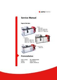
- Page 1 and 2: Service InstructionsDigital Minilab
- Page 3 and 4: List of RegistersEditionRegisterSca
- Page 5 and 6: d-lab.1 family: Circuit DiagramsCon
- Page 7 and 8: d-lab.1 family: Circuit DiagramsCon
- Page 9 and 10: d-lab.1 family: Circuit DiagramsPri
- Page 11: d-lab.1 family
- Page 16 and 17: AGFAPHOTOd-lab.1 family
- Page 18 and 19: AGFAPHOTOd-lab.1 family
- Page 20 and 21: AGFAPHOTOd-lab.1 family
- Page 22 and 23: AGFAPHOTOd-lab.1 family
- Page 24 and 25: AGFAPHOTOd-lab.1 family
- Page 26 and 27: AGFAPHOTOd-lab.1 family
- Page 28 and 29: AGFAPHOTOd-lab.1 family
- Page 30 and 31: AGFAPHOTOd-lab.1 family
- Page 32 and 33: AGFAPHOTOd-lab.1 family
- Page 34 and 35: AGFAPHOTOd-lab.1 family
- Page 36 and 37: AGFAPHOTOd-lab.1 family
- Page 38 and 39: AGFAPHOTOd-lab.1 family
- Page 40 and 41: AE-Z AE-NR DATUM NAMENORMGEPRBEARBD
- Page 42 and 43: AGFAPHOTOd-lab.1 family
- Page 44 and 45: AGFAPHOTOd-lab.1 family
- Page 46 and 47: AGFAPHOTOd-lab.1 family
- Page 48 and 49: d-lab.1 family
- Page 50 and 51: AGFAPHOTOd-lab.1 family
- Page 52 and 53: AGFAPHOTOd-lab.1 family
- Page 54 and 55: AE-Z AE-NR DATUM NAMENORMGEPRBEARBD
- Page 56 and 57: 1.6IIO-BUS+5AR2430R0/1.6IAD-BUS+15A
- Page 58 and 59: AE-Z AE-NR DATUM NAMENORMGEPRBEARBD
- Page 60 and 61: 1.6I/1.6I/1.6IST_BUSAD-BUSIO-BUSR33
- Page 62 and 63:
d-lab.1 family
- Page 64 and 65:
AE-Z AE-NR DATUM NAMENORMGEPRBEARBD
- Page 66 and 67:
AE-Z AE-NR DATUM NAMENORMGEPRBEARBD
- Page 68 and 69:
AGFAPHOTOd-lab.1 family
- Page 70 and 71:
Printed Circuit Boards: Film Proces
- Page 72 and 73:
CN16XASK90F05N249101112345678X65123
- Page 74 and 75:
onmlkjihgTO CPU PCBFCPUCN4123456789
- Page 76 and 77:
CPUFCPU CN1212345678910111290F05N22
- Page 78 and 79:
TO CPUCN10+5VTO SENSERCN11mlk123456
- Page 80 and 81:
mlkjihgfedCN31234567891011121314151
- Page 82 and 83:
R76mlkjihgfedcbaPL+5V/VBTVBTG/PWRFA
- Page 84 and 85:
+5Vmlkjihgfedcba(SHT1)(SHT1)(SHT1)(
- Page 86 and 87:
CN1CN5m5VG/FS1FDRS+5V5VG/MS1FDYS123
- Page 88 and 89:
LS5FLDS/MS3FLDS/LS1FDRS/MS1FLDS/LS8
- Page 90 and 91:
CN1+5V123456R1750S1+5VA+C10.1u/50VA
- Page 92 and 93:
d-lab.1 familyFP 12/MS1FLDS(/MS3FLD
- Page 94 and 95:
CN1LA1FLDLO(LS3FLDLO)LA2FLDLO(LS4FL
- Page 96 and 97:
CS2A-A1AA X 2O1COMSW1NOO2COMSW2NOGS
- Page 98 and 99:
Printed Circuit Boards: Paper Advan
- Page 100 and 101:
BK RD432onmlkjihgfedcbaCS-TIMER1X72
- Page 102 and 103:
4321+24V+24V+5V+5V+5V+5V+5V+5V+5V+5
- Page 104 and 105:
4321PAGE 1PAGE 1SYM. DATE EXCH.No.
- Page 106 and 107:
+3.3V+3.3V+3.3VP+8VGND2P+8VGND2P+8V
- Page 108 and 109:
CD+5VmlkjihgfedcbaCN7SG(AA-15V) 1CN
- Page 110 and 111:
PL+8VTR141R312204CNT(AA+6.5V)(sheet
- Page 112 and 113:
C10.01uF/50V+24V1FS2RXE040GND2+5V4m
- Page 114 and 115:
4MO1ALDPD+5VR7810KTR2R740MO1ALD_AMO
- Page 116 and 117:
+24V4mlkjihg3fedcbaPAVCMO1 APAVCMO1
- Page 118 and 119:
4321+5VGND2+5V+36V+5VGND2+24V+5V+5V
- Page 120 and 121:
abcdfeghjiklmabcdfeghjiklmabcdfeghj
- Page 122 and 123:
DB10DB11DB12DB13DB14DB15DB9DB8+5VGN
- Page 124 and 125:
DB9DB10DB13DB11DB15DB9DB15DB15DB14D
- Page 126 and 127:
d-lab.1 familyAP 205V(Cont.)OUT85VG
- Page 128 and 129:
OUT+5V5VGCN1231+5VR1200 1/8W+S1C1AO
- Page 130 and 131:
OUT2OUT1+5V5VGCN12341+5VR2150R1150R
- Page 132 and 133:
WDTCN4213UL1007 AWG24 OGUL1007 AWG2
- Page 134 and 135:
Printed Circuit Boards: Paper Proce
- Page 136 and 137:
4MEASURING HEADDENSCONTROLPCBCN3CN3
- Page 138 and 139:
YWYWSMP-02V-BCDRY SW12PRO SW1290P16
- Page 140 and 141:
A4mlkjihg3fCN1321B3B-XH-AGU+5VOUT34
- Page 142 and 143:
4mlkjihg32fedcbaCN2CN41-178314-3123
- Page 144 and 145:
2These parts aren't mounted with a
- Page 146 and 147:
+8V-8V-8V+8V+8V-8V+8V-8V+3.3V+8VAN0
- Page 148 and 149:
+5V+5V+3.3V+5V+3.3V+5V+3.3V+5V+5V+3
- Page 150 and 151:
1These parts aren't mounted with a
- Page 152 and 153:
+5VR55R5610K10KCN712345678910HIF3FC
- Page 154 and 155:
24VGNC+24VCN11231-178313-32D113D8LC
- Page 156 and 157:
mlkjihgfedcbTO FPRR1680STB. HTD1TLR
- Page 158 and 159:
onmlkjihgfedcbaN5284 90A-TB2 (P4-44
- Page 160 and 161:
d-lab.1 family: Circuit DiagramsPri
- Page 162 and 163:
4onmlkjihg3fedcba2EXPOSURE TABLE UN
- Page 164 and 165:
43215VCON5VCON+5V+24VGND2+36VGND2+5
- Page 166 and 167:
43onmlkjihgf90A05N1990A05N20CPUCN12
- Page 168 and 169:
4onmlkjihg3fedcba2PROCESSING BLOCKP
- Page 170 and 171:
43onmlkjihgfedcbaDRY INTER LOCKPPDH
- Page 172 and 173:
TB1-1PPCTHT01PPCTHT02PPCTHT05WTWTWT
- Page 174 and 175:
4MEASURING HEADDENSCONTROLPCBCN3CN3
- Page 176 and 177:
YWYWSMP-02V-BCDRY SW12PRO SW1290P16