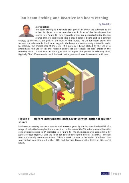
Ion beam Etching and Reactive Ion beam etching
Ion beam Etching and Reactive Ion beam etching
Ion beam Etching and Reactive Ion beam etching
- No tags were found...

You also want an ePaper? Increase the reach of your titles
YUMPU automatically turns print PDFs into web optimized ePapers that Google loves.
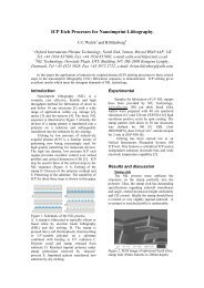
<strong>Ion</strong> <strong>beam</strong> <strong>Etching</strong> <strong>and</strong> <strong>Reactive</strong> <strong>Ion</strong> <strong>beam</strong> <strong>etching</strong>By Tim JollyIntroduction<strong>Ion</strong> <strong>beam</strong> <strong>etching</strong> is a versatile etch process in which the substrate to beetched is placed in a vacuum chamber in front of the broad-<strong>beam</strong> ionsource (see Figure 1). <strong>Ion</strong>s (typically argon) are generated inside the ionsource <strong>and</strong> are accelerated into a broad parallel <strong>beam</strong>, <strong>and</strong> to a definedenergy, by the extraction grids on the front of the source. As the ion <strong>beam</strong> etches thesurface, the substrate is tilted to an angle in the <strong>beam</strong> <strong>and</strong> continuously rotated in orderto optimize the smoothness of the etch. If a pattern is being etched by the use of aphotomask, the use of tilt <strong>and</strong> rotation allows the user adjust the wall angles in theresulting etch. If one uses an inert gas such as argon, the process is relatively slow,(typically 50 - 100nm/minute,) <strong>and</strong> the heat that is generated must be removed with care.Figure 1sourceOxford Instruments <strong>Ion</strong>fab300Plus with optional sputter<strong>Ion</strong> <strong>beam</strong> processing has been transformed in recent years by the introduction by OIPT of arange of inductively-coupled ion sources that in the case of the 35cm ion source allows theetch of substrates up to 8” diameter (see Figure 2). The 35cm ion source uses a 2MHz RFgenerator (see Figure 3) <strong>and</strong> the 15cm ion source (see Figure 4) uses 13.56MHz. The ionsource is virtually maintenance-free. This is in stark contrast to the earlier “Kaufman” ionsources that were first used in the 1970s <strong>and</strong> that had filaments that lasted as little as 10hours.October 2003 ⏐ Page 1
Figure 2Typical etch uniformity with 30cm ion <strong>beam</strong>Figure 3Oxford Instruments 35cm ion sourceOctober 2003 ⏐ Page 2
Figure 4Oxford Instruments 15cm ion source<strong>Ion</strong>fab300PlusThe Oxford Instruments <strong>Ion</strong>fab300Plus represents the state of the art for ion <strong>beam</strong> <strong>etching</strong>.It takes the 15cm or 35cm ion source, <strong>and</strong> has a loadlock so that throughput is greatlyincreased, <strong>and</strong> processing can be cassette-to-cassette if necessary, see Figure 5. Theloadlock is to st<strong>and</strong>ard “MESC” specification, so that this system can be built into clusterswith other process chambers from Oxford Instruments or other vendors.Figure 5Oxford Instruments <strong>Ion</strong>fab300Plus with loadlockAs an argon ion <strong>beam</strong> <strong>etching</strong> system, the 300Plus is used for <strong>etching</strong> materials such asgold or platinum, cadmium mercury telluride (CMT), indium phosphide (InP) or aluminiumgallium arsenide (AlGaAs) The chief advantage of the process is that it will etch throughall materials. A typical example of its advantage is when <strong>etching</strong> a multilayer stack ofalternate layers of GaAs <strong>and</strong> AlGaAs. The ion <strong>beam</strong> process will etch through all of thelayers with minimum deviation in the wall angle.October 2003 ⏐ Page 3
In an argon ion <strong>beam</strong> etch, it is inevitable that heat will be generated in the substrate bythe ion <strong>beam</strong>, as a high energy of ion is needed. In fact, in many materials, the minimumheat is generated by the use of ions with an energy of around 600V. The 300Plus useshelium cooling of the wafer backside to remove the heat.<strong>Reactive</strong> <strong>Ion</strong> Beam <strong>Etching</strong>A major advantage of the RF ion source, is that you can perform reactive etches by feedinggases such as Cl2, F2, CF4, O2 directly into the ion source. This process is known as <strong>Reactive</strong><strong>Ion</strong> Beam <strong>Etching</strong> (RIBE). The gases are cracked in the ion source, <strong>and</strong> the positive speciesare extracted into the ion <strong>beam</strong>, see Figure 6. Again, unlike the older Kaufman ion source,source reliability is not affected by the use of such gases. The process that results will bepartially chemical, as the ions react with the surface, <strong>and</strong> partially physical, as the reactionproducts are sputtered away by the energy of the ion flux. An evident advantage of RIBEis that the relative importance of these processes can be changed by adjusting the ionenergy. Typical RIBE processes include CMT, GaAs, InP, see Figure 7.Figure 6 Cracking pattern of SF6 gas in Oxford Instruments ionsource courtesy of Stefan SchneiderFigure 7<strong>Ion</strong> <strong>beam</strong> <strong>etching</strong> a substrateOctober 2003 ⏐ Page 4
Flexibility<strong>Ion</strong> <strong>beam</strong> <strong>etching</strong> systems are uniquely capable of developing new processes, since all ofthe parameters are directly <strong>and</strong> independently controlled: ion energy; ion flux density;angle of incidence; process chamber pressure; substrate temperature. It is fair to note thatfor high volume production, the process will generally need to be transferred to anothertechnology - generally a plasma system -- in order to reduce the production costs. Hence,for example, almost no mainstream silicon production steps are performed with ion <strong>beam</strong>.However, for a number of complex processes, where it is too difficult or simply not costeffectiveto attempt to transfer the process to another technology, ion <strong>beam</strong> <strong>etching</strong> orRIBE will remain the process of choice.OIPT supply both ion <strong>beam</strong> systems <strong>and</strong> plasma etch systems. Our ICP plasma etch systemshave similar capabilities. In the ICP380, for example, a plasma is generated in a chamberabove the substrate that is to be etched, <strong>and</strong> ions are accelerated down onto the substrateby applying RF power onto the table that holds the substrate. The process is known as<strong>Reactive</strong> <strong>Ion</strong> <strong>Etching</strong> (RIE) although in fact it is possible to use argon for an inert etch. Thefollowing table highlights some of the differences between ion <strong>beam</strong> <strong>etching</strong>, RIBE <strong>and</strong>plasma <strong>etching</strong>.Process ResearchAdvantages of <strong>Ion</strong>Beam <strong>Etching</strong>Advantages of ICP EtchApplications<strong>Ion</strong> Beam Etch <strong>and</strong> RIBEFundamental reseach into processphysics <strong>and</strong> chemistry in ion <strong>beam</strong>systems helps us to underst<strong>and</strong> ICP aswell as ion <strong>beam</strong> processes. <strong>Ion</strong> <strong>beam</strong>remains an important productionprocess in its own right.All parameters can be setindependently for rapid processoptimization.Inert <strong>etching</strong> with variable incidence tooptimize the etch process. <strong>Ion</strong> enegycan be adjusted 20eV – 1500eV.Etch process is face-down, which canimprove process cleanliness.Mainstream production of specialist III-V devicies. Mainstream <strong>etching</strong> ofmaterials such as CMT <strong>and</strong> V2O5.Production <strong>etching</strong> of Au <strong>and</strong> Ptstructures <strong>and</strong> multilayer devices.ICP EtchProcess developmentproceeds by empiricalresearch <strong>and</strong> processmodellingProcess parameters areadjustable but cannot beset independently. Forexample, increasing gasflow will affect chamberpressure, plasma density,bias voltage etc.Inert <strong>etching</strong> possible, butresults limited by the useof normal incidence.Etch process is face-up<strong>Reactive</strong> processing canetch most materials atlower energy <strong>and</strong>(sometimes) with lowerdamage. Faster speedsAt great expense, certainICP processes have beendeveloped that allowunmatchable results; forexample in the case of the“Bosh” process, deepstructures with verticalwalls.Mainstream processing ofSi for semiconductor <strong>and</strong>MEMS markets.Mainstream processing ofGaAs etcOctober 2003 ⏐ Page 5