Electrical characterisation of Transistors - Stallinga.org
Electrical characterisation of Transistors - Stallinga.org
Electrical characterisation of Transistors - Stallinga.org
- No tags were found...

Create successful ePaper yourself
Turn your PDF publications into a flip-book with our unique Google optimized e-Paper software.
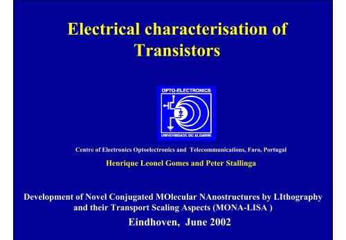
<strong>Electrical</strong> <strong>characterisation</strong> <strong>of</strong><strong>Transistors</strong>Centre <strong>of</strong> Electronics Optoelectronics and Telecommunications, Faro, PortugalHenrique Leonel Gomes and Peter <strong>Stallinga</strong>Development <strong>of</strong> Novel Conjugated MOlecular NAnostructures by LIthographyand their Transport Scaling Aspects (MONA-LISA )Eindhoven, June 2002
Areas <strong>of</strong> research• Semiconductor and device assessment.We mainly consider a wide range <strong>of</strong> experiments designedto measure essential parameters such as:– Free carrier density– Field effect mobility– Donor and acceptor densities.– Deep level and interface state densities.
• Device performance.Outline• Charge transport mechanisms.• Stability and reability issues(effects <strong>of</strong> traps and interfacial problems).
Interactions with MONA-LISA PartnersPhilipsElectronicsBolonhaFaroWurzburg
DLTS ExperimentsVg=-20 V0.8Vg=0V-Ids(A)0.60.4VDS=-0.5Vn-Si0.21 x 10-6 -Vds (V)Bulk traps N bs(E)Interface traps N is(E)00 2 4 6 8S( t)= A0−A1−NNTD1[ 1−exp( −t/ τ )]S( t)= A0 − A 1−exp( −t/ τ )The transient has not anexponential decayOverlap <strong>of</strong> responses times from several close traps.Large density <strong>of</strong> traps.Different traps in different regions <strong>of</strong> the device.20
DLTS Experiments4.5 x 10-11 Temperature (K)4DLTS Signal (Arb. Unit)3.532.52t1/t2 (sec)5/25Vds=-0.5 VVg=from -20 V to 0 V1.51190 200 210 220 230 240 250 260 270 280 290DLTS spectra <strong>of</strong> drain-current transients due to gate biaspulse from –20V to 0 V.
The effect on the device characteristcsAnnealed stateStressed stateMobility (cm 2 V -1 s -1)Threshold voltage (V)1.1x10 -3 8.9x10 -50.6 18.2
The effect on the device characteristcs35A G4.M1Mobility=2.7x10-21.2 x 10-5 Applied gate voltage (V)cm2V-1 s-10.8Drain current (A)0.60.4Annealed0.2As received0-10 -5 0 5 10 15 20
Negative VgWhat we knowHigher threshold voltage.Causes degradation. Lower mobility.Decrease in the drain current.Positive VgTends to restore devicedegradation.Annealingunder positive VgInduces a high Drain Leakage Current(GIDL current).Repairs device degradation caused by thenegative gate stress.
Where are located (in the device geometry ) the stress inducedcharges ?Organic Layer+/- +/- +/- +/- +/-+ + + + +SiO 2Induced interface states ?Oxide Charges ?Both ?The degradation in conventionaln-MOS can be described by apower-law over time, with theexponent usually being in therange <strong>of</strong> 2/3.Log Im=2/3Log (Time)
Device relaxation (time constants)Annealed stateτ 1 =20 sτ 2 =40 min.cNormal state
Device relaxation (time constants)Normal stateτ 1 =10 sτ 2 =2.8 HoursVg=-3VStressed state
Relaxation from an annealed state to a normal state.120100Vds= - 0.5 VInitial stage- Drain-Source Current (nA)806040cafter 4 hoursafter 15.5 hoursafter 25 hoursafter 62 hours2000 5 10 15 20 25 30- Gate Voltage Vg (V)
Relaxation from an annealed state to a normal state.120- Drain-Source Current (nA)1101009080706050Vds= - 0.5 VVg= - 20 V40300 10 20 30 40 50 60Time(Hours)
Temperature dependence <strong>of</strong> the drain current under anapplied gate voltage <strong>of</strong> –20 V454035Vds = -0.5 VVg = -20 V30Current (nA)2520151050100 150 200 250 300 350Temperature (K)
Characterization <strong>of</strong> stress-induced traps by using asubthreshold current techniqueS =kT ⎛S ln10.⎜1+q ⎝STdVGln10.d ln I= ACi=SO1+.D( CA1+C+CA⎞⎟⎠Cit/ C) / CiiWhere:C A is the capaciatnce <strong>of</strong> theaccumulation layerCi is the oxide capacitanceCit is the capacitance due to interfacestate density.Nit=7x10 -11 cm -2 J.H. Schön and B. Batlogg (J. Appl. Phys., Vol 89, 336 (2001))
-16Nit=1.4x10 -11 cm -2 .FT17.MLn (Drain current) (A)-18-20-22-24Vst= -1 VVst= -18 V-26-280 5 10 15Gate Voltage (v)
Stress induced interface state density6Interface state density (cm-2)543211012 0-10 5 10 15 20 257 x Abs (stress voltage) (V)
FT21.M1.2 x 10-7 Gate Voltage (V)Vst = -22 VDrain Current (A)10.80.60.4The mobilityremains constant !Vst = -21 VVst = -19 VVst = -18 VVst = -16 VVst = -15 V0.200 5 10 15 20
Carrier scattering within the grain boundary region can be lumpedinto the effective mobility modelPseudo-Subthreshold CharacteristicsGrain Boundry regionGrain barrierlowering effectsSiO 2In poly-Si TFTThe exponential dependence <strong>of</strong> the drian current on the gate voltage isdue to the gate induced grain barrier lowering effects, and not due tothe accumulation charge density modulated by the gate as the singleSi-MOSFET does
Mechanisms for the GIDL current‣ Oxide charges shifts the flat-band voltage andresults in an enchanced <strong>of</strong> the GIDL current.‣ Generation <strong>of</strong> interface states may introduceadditional band-trap-band leakage mechanisms
Frequency dependent transfer curves(evidences for fast interface states!)9 x 10⁻⁸ -Vg (V)81000 mV/s76-Ids (A)5433 mV/s321Increasing scanningspeed00 2 4 6 8 10 12 14
Thermally Stimulated Currents (TSC)2.2 x 10⁻¹² Temperature (K)21.8Vg=+ 20 V1.6Current (A)1.41.210.80.60.4100 150 200 250 300 350
ConclusionsDegradation is a very complex problem and depends on many(possibly not a priori know) technology-sensitive parameters, s<strong>of</strong>urther experimental material has to be collected to determine themodel parameters.