Electrical characterisation of Transistors - Stallinga.org
Electrical characterisation of Transistors - Stallinga.org
Electrical characterisation of Transistors - Stallinga.org
SHOW LESS
- No tags were found...

You also want an ePaper? Increase the reach of your titles
YUMPU automatically turns print PDFs into web optimized ePapers that Google loves.
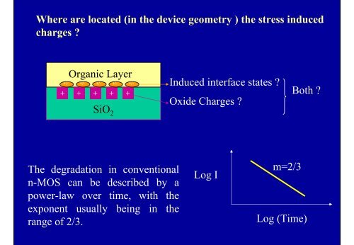
Where are located (in the device geometry ) the stress inducedcharges ?Organic Layer+/- +/- +/- +/- +/-+ + + + +SiO 2Induced interface states ?Oxide Charges ?Both ?The degradation in conventionaln-MOS can be described by apower-law over time, with theexponent usually being in therange <strong>of</strong> 2/3.Log Im=2/3Log (Time)