Optoisolator triac driver output - todopic
Optoisolator triac driver output - todopic
Optoisolator triac driver output - todopic
- No tags were found...

Create successful ePaper yourself
Turn your PDF publications into a flip-book with our unique Google optimized e-Paper software.
I ELECTRICAL CHARACTERISTICS (TA = 25°C unless otherwise noted)INPUT LEDReverse Leakage Current(VR = 6 V)Forward Voltage(IF = 30 mA)OUTPUT DETECTOR (IF = 0 unless otherwise noted)Leakage with LED Off, Either Direction(Rated VDRM (1) )Peak On–State Voltage, Either Direction(ITM = 100 mA Peak)Characteristic Symbol Min Typ Max UnitIR — 0.05 100 µAVF — 1.3 1.5 VoltsIDRM1 — 2 100 nAVTM — 1.8 3 VoltsCritical Rate of Rise of Off–State Voltage(3) dv/dt 1000 2000 — V/µsCOUPLEDLED Trigger Current, Current Required to Latch Output(Main Terminal Voltage = 3 V(2))MOC3041MOC3042MOC3043Holding Current, Either Direction IH — 250 — µAIsolation Voltage (f = 60 Hz, t = 1 sec) VISO 7500 — — Vac(pk)ZERO CROSSINGInhibit Voltage(IF = Rated IFT, MT1–MT2 Voltage above which device willnot trigger.)Leakage in Inhibited State(IF = Rated IFT, Rated VDRM, Off State)IFT——————15105mAVIH — 5 20 VoltsIDRM2 — — 500 µA1. Test voltage must be applied within dv/dt rating.2. All devices are guaranteed to trigger at an IF value less than or equal to max IFT. Therefore, recommended operating IF lies between IFT2. (15 mA for MOC3041, 10 mA for MOC3042, 5 mA for MOC3043) and absolute max IF (60 mA).3. This is static dv/dt. See Figure 7 for test circuit. Commutating dv/dt is a function of the load–driving thyristor(s) only.TYPICAL ELECTRICAL CHARACTERISTICSTA = 25°CTM, ON-STATE CURRENT (mA)+800+600+400+2000–200–400–600–800OUTPUT PULSE WIDTH – 80 µsIF = 30 mAf = 60 HzTA = 25°CNORMALIZED IFT1.51.41.31.21.110.90.80.7NORMALIZED TOTA = 25°C–4–3–2 –1 0 1 2 3VTM, ON–STATE VOLTAGE (VOLTS)45–40–20 0 20 40 60 80TA, AMBIENT TEMPERATURE (°C)Figure 1. On–State CharacteristicsFigure 2. Trigger Current versus Temperature2 Motorola Optoelectronics Device Data
VCCRin 123MOC3041/3042/3043654330360 Ω390.01LOADHOT240 VacNEUTRAL* For highly inductive loads (power factor < 0.5), change this value to360 ohms.Typical circuit for use when hot line switching is required.In this circuit the “hot” side of the line is switched and theload connected to the cold or neutral side. The load may beconnected to either the neutral or hot line.Rin is calculated so that IF is equal to the rated IFT of thepart, 5 mA for the MOC3043, 10 mA for the MOC3042, or15 mA for the MOC3041. The 39 ohm resistor and 0.01 µFcapacitor are for snubbing of the <strong>triac</strong> and may or may notbe necessary depending upon the particular <strong>triac</strong> and loadused.Figure 8. Hot–Line Switching Application Circuit240 VacVCCRin123MOC3041/3042/3043R1654D1360 ΩSCRSCRSuggested method of firing two, back–to–back SCR’s,with a Motorola <strong>triac</strong> <strong>driver</strong>. Diodes can be 1N4001; resistors,R1 and R2, are optional 330 ohms.NOTE: This optoisolator should not be used to drive a load directly.It is intended to be a trigger device only.R2D2LOADFigure 9. Inverse–Parallel SCR Driver Circuit4 Motorola Optoelectronics Device Data
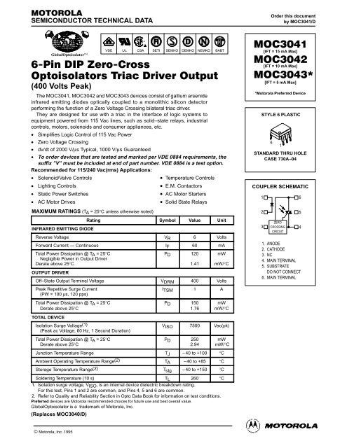
PACKAGE DIMENSIONS –A–6 41 3–B–NOTES:1. DIMENSIONING AND TOLERANCING PER ANSIY14.5M, 1982.2. CONTROLLING DIMENSION: INCH.3. DIMENSION L TO CENTER OF LEAD WHENFORMED PARALLEL.–T–SEATINGPLANEF 4 PLE 6 PLNC LKGMD 6 PL0.13 (0.005) M T A M B MJ 6 PL0.13 (0.005) M T B M A MINCHES MILLIMETERSDIM MIN MAX MIN MAXA 0.320 0.350 8.13 8.89B 0.240 0.260 6.10 6.60C 0.115 0.200 2.93 5.08D 0.016 0.020 0.41 0.50E 0.040 0.070 1.02 1.77F 0.010 0.014 0.25 0.36G 0.100 BSC 2.54 BSCJ 0.008 0.012 0.21 0.30K 0.100 0.150 2.54 3.81L 0.300 BSC 7.62 BSCM 0 15 0 15N 0.015 0.100 0.38 2.54STYLE 6:PIN 1. ANODE2. CATHODE3. NC4. MAIN TERMINAL5. SUBSTRATE6. MAIN TERMINALCASE 730A–04ISSUE G–A–6143–B–NOTES:1. DIMENSIONING AND TOLERANCING PER ANSIY14.5M, 1982.2. CONTROLLING DIMENSION: INCH.F 4 PLE 6 PLGHD 6 PLCLK 6 PL0.13 (0.005) M T A M B MJ–T–SEATINGPLANE0.13 (0.005) M T B M A MCASE 730C–04ISSUE DINCHES MILLIMETERSDIM MIN MAX MIN MAXA 0.320 0.350 8.13 8.89B 0.240 0.260 6.10 6.60C 0.115 0.200 2.93 5.08D 0.016 0.020 0.41 0.50E 0.040 0.070 1.02 1.77F 0.010 0.014 0.25 0.36G 0.100 BSC 2.54 BSCH 0.020 0.025 0.51 0.63J 0.008 0.012 0.20 0.30K 0.006 0.035 0.16 0.88L 0.320 BSC 8.13 BSCS 0.332 0.390 8.43 9.90*Consult factory for leadformoption availabilityMotorola Optoelectronics Device Data5
F 4 PL–T–SEATINGPLANE–A–6 4–B–1 3NLCG KD 6 PLJNOTES:1. DIMENSIONING AND TOLERANCING PER ANSIY14.5M, 1982.2. CONTROLLING DIMENSION: INCH.3. DIMENSION L TO CENTER OF LEAD WHENFORMED PARALLEL.INCHES MILLIMETERSDIM MIN MAX MIN MAXA 0.320 0.350 8.13 8.89B 0.240 0.260 6.10 6.60C 0.115 0.200 2.93 5.08D 0.016 0.020 0.41 0.50E 0.040 0.070 1.02 1.77F 0.010 0.014 0.25 0.36G 0.100 BSC 2.54 BSCJ 0.008 0.012 0.21 0.30K 0.100 0.150 2.54 3.81L 0.400 0.425 10.16 10.80N 0.015 0.040 0.38 1.02E 6 PL0.13 (0.005) M T A M B M*Consult factory for leadformoption availabilityCASE 730D–05ISSUE DMotorola reserves the right to make changes without further notice to any products herein. Motorola makes no warranty, representation or guarantee regardingthe suitability of its products for any particular purpose, nor does Motorola assume any liability arising out of the application or use of any product or circuit,and specifically disclaims any and all liability, including without limitation consequential or incidental damages. “Typical” parameters can and do vary in differentapplications. All operating parameters, including “Typicals” must be validated for each customer application by customer’s technical experts. Motorola doesnot convey any license under its patent rights nor the rights of others. Motorola products are not designed, intended, or authorized for use as components insystems intended for surgical implant into the body, or other applications intended to support or sustain life, or for any other application in which the failure ofthe Motorola product could create a situation where personal injury or death may occur. Should Buyer purchase or use Motorola products for any suchunintended or unauthorized application, Buyer shall indemnify and hold Motorola and its officers, employees, subsidiaries, affiliates, and distributors harmlessagainst all claims, costs, damages, and expenses, and reasonable attorney fees arising out of, directly or indirectly, any claim of personal injury or deathassociated with such unintended or unauthorized use, even if such claim alleges that Motorola was negligent regarding the design or manufacture of the part.Motorola and are registered trademarks of Motorola, Inc. Motorola, Inc. is an Equal Opportunity/Affirmative Action Employer.How to reach us:USA / EUROPE: Motorola Literature Distribution;JAPAN: Nippon Motorola Ltd.; Tatsumi–SPD–JLDC, Toshikatsu Otsuki,P.O. Box 20912; Phoenix, Arizona 85036. 1–800–441–2447 6F Seibu–Butsuryu–Center, 3–14–2 Tatsumi Koto–Ku, Tokyo 135, Japan. 03–3521–8315MFAX: RMFAX0@email.sps.mot.com – TOUCHTONE (602) 244–6609 HONG KONG: Motorola Semiconductors H.K. Ltd.; 8B Tai Ping Industrial Park,INTERNET: http://Design–NET.com 51 Ting Kok Road, Tai Po, N.T., Hong Kong. 852–266292986 ◊Motorola Optoelectronics MOC3041/D Device Data