LM1815 Adaptive Variable Reluctance Sensor Amplifier - Not2Fast
LM1815 Adaptive Variable Reluctance Sensor Amplifier - Not2Fast
LM1815 Adaptive Variable Reluctance Sensor Amplifier - Not2Fast
- No tags were found...

Create successful ePaper yourself
Turn your PDF publications into a flip-book with our unique Google optimized e-Paper software.
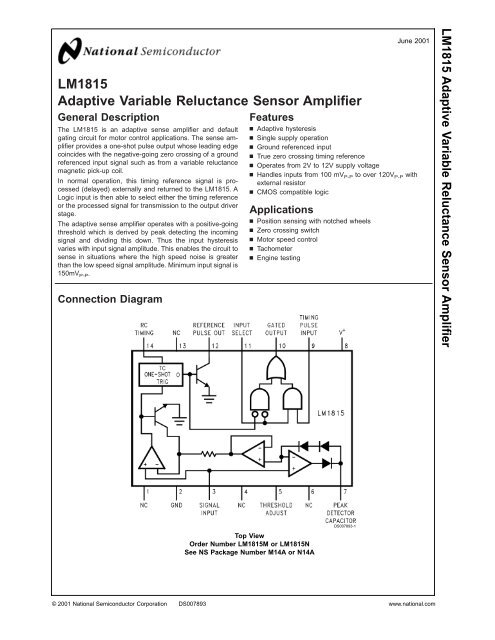
<strong>LM1815</strong><strong>Adaptive</strong> <strong>Variable</strong> <strong>Reluctance</strong> <strong>Sensor</strong> <strong>Amplifier</strong>General DescriptionThe <strong>LM1815</strong> is an adaptive sense amplifier and defaultgating circuit for motor control applications. The sense amplifierprovides a one-shot pulse output whose leading edgecoincides with the negative-going zero crossing of a groundreferenced input signal such as from a variable reluctancemagnetic pick-up coil.In normal operation, this timing reference signal is processed(delayed) externally and returned to the <strong>LM1815</strong>. ALogic input is then able to select either the timing referenceor the processed signal for transmission to the output driverstage.The adaptive sense amplifier operates with a positive-goingthreshold which is derived by peak detecting the incomingsignal and dividing this down. Thus the input hysteresisvaries with input signal amplitude. This enables the circuit tosense in situations where the high speed noise is greaterthan the low speed signal amplitude. Minimum input signal is150mV P-P .Connection DiagramFeaturesn <strong>Adaptive</strong> hysteresisn Single supply operationn Ground referenced inputn True zero crossing timing referencen Operates from 2V to 12V supply voltagen Handles inputs from 100 mV P-P to over 120V P-P withexternal resistorn CMOS compatible logicApplicationsn Position sensing with notched wheelsn Zero crossing switchn Motor speed controln Tachometern Engine testingJune 2001<strong>LM1815</strong> <strong>Adaptive</strong> <strong>Variable</strong> <strong>Reluctance</strong> <strong>Sensor</strong> <strong>Amplifier</strong>Top ViewOrder Number <strong>LM1815</strong>M or <strong>LM1815</strong>NSee NS Package Number M14A or N14ADS007893-1© 2001 National Semiconductor Corporation DS007893 www.national.com
<strong>LM1815</strong>Absolute Maximum Ratings (Note 1)If Military/Aerospace specified devices are required,please contact the National Semiconductor Sales Office/Distributors for availability and specifications.Supply VoltagePower Dissipation (Note 2)12V1250 mWOperating Temperature RangeStorage Temperature RangeJunction TemperatureInput CurrentLead Temperature(Soldering, 10 sec.)−40˚C ≤ T A ≤ +125˚C−65˚C ≤ T J ≤ +150˚C+150˚C±30 mA260˚CElectrical Characteristics (T A = 25˚C, V CC = 10V, unless otherwise specified, see Figure 1)Parameter Conditions Min Typ Max UnitsOperating Supply Voltage 2.5 10 12 VSupply Current f IN = 500 Hz, Pin 9 = 2V, Pin 11 = 0.8V 3.6 6 mAReference Pulse Width f IN = 1 Hz to 2 kHz, R = 150kΩ, C=0.00µF70 100 130 µsLogic Input Bias Current V IN = 2V, (Pin 9 and Pin 11) 5 µASignal Input Bias Current V IN = 0V dc, (Pin 3) 200 nAInput Impedance V IN = 5 Vrms, (Note 3) 12 20 28 kΩZero Crossing Threshold V IN = 100 mV P-P , (Pin 3) 25 mVLogic Threshold (Pin 9 and Pin 11) 0.8 1.1 2.0 VV OUT High R L =1kΩ, (Pin 10) 7.5 8.6 VV OUT Low I SINK = 0.1 mA, (Pin 10) 0.3 0.4 VInput Arming Threshold Pin 5 Open, V IN = 135 mV P-P (Mode 1) 30 45 60 mVPin 5 Open, V IN ≥ 230 mV P-P (Mode 1) 40 80 90 % of V 3 +P KPin5toV + ,V IN ≥ 1V P-P (Mode 2) 200 300 450 mVPin 5 to Gnd, V IN ≥ 100mV P-P (Mode 3) −25 0 25 mVOutput Leakage Pin 12 V 12 = 11V 0.01 10 µASaturation Voltage P12 I 12 = 2 mA 0.2 0.4 VNote 1: “Absolute Maximum Ratings” are those values beyond which the safety of the device cannot be guaranteed. They are not meant to imply that the devicesshould be operated at these limits. The table of “Electrical Characteristics” specifies conditions of device operation.Note 2: For operation at elevated temperatures, the device must be derated based on a 150˚C maximum junction temperature and a thermal resistance of 80˚C/W(DIP), 120˚C/W (SO-14) junction to ambient.Note 3: Measured at input to external 18 kΩ resistor. IC contains 1 kΩ in series with diode to attenuate the input signal.Truth TableSignalInputPin 3RCTimingPin 14InputSelectPin 11TimingInputPin 9GatedOutputPin 10± Pulses RC L X Pulses = RCX X H H HX X H L L± Pulses L L L ZeroCrossingwww.national.com 2
Truth Table (Continued)<strong>LM1815</strong>FIGURE 1. <strong>LM1815</strong> <strong>Adaptive</strong> Sense <strong>Amplifier</strong>DS007893-23www.national.com
<strong>LM1815</strong>Schematic DiagramDS007893-4www.national.com 4
Application Hints<strong>LM1815</strong>FIGURE 2. <strong>LM1815</strong> OscillogramsDS007893-3Input Voltage ClampThe signal input voltage at pin 3 is internally clamped. Currentlimit for the Input pin is provided by an external resistorwhich should be selected to allow a peak current of ±3mAinnormal operation. Positive inputs are clamped by a 1 kohmresistor and series diode (see R4 and Q12 in the internalschematic diagram), while an active clamp limits pin 3 totypically 350mV below Ground for negative inputs (see R2,R3, Q10, and Q11 in the internal schematic diagram). Thusfor input signal transitions that are more than 350mV belowGround, the input pin current (up to 3mA) will be pulled fromthe V+ supply. If the V+ pin is not adequately bypassed theresulting voltage ripple at the V+ pin will disrupt normaldevice operation. Likewise, for input signal transitions thatare more than 500mV above Ground, the input pin currentwill be dumped to Ground through device pin 2. Slight shiftsin the Ground potential at device pin 2, due to poor groundingtechniques relative to the input signal ground, can causeunreliable operation. As always, adequate device grounding,and V+ bypassing, needs to be considered across the entireinput voltage and frequency range for the intended application.Input Current LimitingAs stated earlier, current limiting for the Input pin is providedby a user supplied external resistor. For purposes of selectingthe appropriate resistor value the Input pin should beconsidered to be a zero ohm connection to ground. Forapplications where the input voltage signal is not symmetricalwith relationship to Ground the worst case voltage peakshould be used.Minimum Rext = ((Vin peak)/3mA)In the application example shown in figure 1(Rext=18kohms) the recommended maximum input signalvoltage is ±54V (i.e. 108Vp-p).Operation of Zero Crossing DetectorThe <strong>LM1815</strong> is designed to operate as a zero crossingdetector, triggering an internal one shot on thenegative-going edge of the input signal. Unlike other zerocrossing detectors, the <strong>LM1815</strong> cannot be triggered until theinput signal has crossed an ’arming’ threshold on thepositive-going portion of the waveform. The arming circuit isreset when the chip is triggered, and subsequent zero crossingsare ignored until the arming threshold is exceededagain. This threshold varies depending on the connection atpin 5. Three different modes of operation are possible:MODE 1, Pin 5 openThe adaptive mode is selected by leaving device pin 5 opencircuit. For input signals of less than ±135mV (i.e. 270mVp-p) and greater than typically ±75mV (i.e. 150mVp-p),the input arming threshold is typically at 45mV. Under theseconditions the input signal must first cross the 45mV thresholdin the positive direction to arm the zero crossing detector,and then cross zero in the negative direction to trigger it.If the signal is less than 30mV peak (minimum rating inElectrical Characteristics), the one shot is guaranteed to nottrigger.Input signals of greater than ±230mV (i.e. 460 mVp-p) willcause the arming threshold to track at 80% of the peak inputvoltage. A peak detector capacitor at device pin 7 stores avalue relative to the positive input peaks to establish thearming threshold. Input signals must exceed this threshold inthe positive direction to arm the zero crossing detector,which can then be triggered by a negative-going zero crossing.The peak detector tracks rapidly as the input signal amplitudeincreases, and decays by virtue of the resistor connectedexternally at pin 7 track decreases in the input signal.If the input signal amplitude falls faster than the voltagestored on the peak detector capacitor there may be a loss ofoutput signal until the capacitor voltage has decayed to anappropriate level.Note that since the input voltage is clamped, the waveformobserved at pin 3 is not identical to the waveform observedat the variable reluctance sensor. Similarly, the voltagestored at pin 7 is not identical to the peak voltage appearingat pin 3.MODE 2, Pin 5 connected to V+.The input arming threshold is fixed at 200mV minimum whendevice pin 5 is connected to the positive supply. The chip has5www.national.com
<strong>LM1815</strong>Application Hints (Continued)no output for signals of less than ±200 mV (i.e. 400mVp-p)and triggers on the next negative-going zero crossing whenthe arming threshold is has been exceeded.MODE 3, Pin 5 grounded.With pin 5 grounded, the input arming threshold is set to 0V,±25mV maximum. Positive-going zero crossings arm thechip, and the next negative-going zero crossing triggers it.This is the very basic form of zero-crossing detection.One Shot TimingThe one shot timing is set by a resistor and capacitor connectedto pin 14. The recommended maximum resistor valueis 150kohms. The capacitor value can be changed asneeded, as long as the capacitor type does not present anysignfigant leakage that would adversely affect the RC timeconstant.The output pulse width is:pulse width = 0.673 xRxC (1)For a given One Shot pulse width, the recommended maximuminput signal frequency is:Fin(max) = 1/(1.346 xRxC) (2)In the application example shown in figure 1 (R=150kohms,C=0.001µF) the recommended maximum input frequencywill typically be 5kHz. Operating with input frequenciesabove the recommended Fin (max) value may result inunreliable performance of the One Shot circuitry. For thoseapplications where the One Shot circuit is not required,device pin 14 can be tied directly to Ground.Logic InputsIn some systems it is necessary to externally generatepulses, such as during stall conditions when the variablereluctance sensor has no output. External pulse inputs at pin9 are gated through to pin 10 when Input Select (pin 11) ispulled high. Pin 12 is a direct output for the one shot and isunaffected by the status of pin 11.Input/output pins 9, 11, 10, and 12 are all CMOS logiccompatible. In addition, pins 9, 11, and 12 are TTL compatible.Pin 10 is not guaranteed to drive a TTL load.Pins 1, 4, 6 and 13 have no internal connections and can begrounded.www.national.com 6
Physical Dimensions inches (millimeters) unless otherwise noted<strong>LM1815</strong>14-Lead Small Outline Circuit (M)Order Number <strong>LM1815</strong>MNS Package Number M14AMolded Dual-In-Line Package (N)Order Number <strong>LM1815</strong>NNS Package Number N14A7www.national.com
<strong>LM1815</strong> <strong>Adaptive</strong> <strong>Variable</strong> <strong>Reluctance</strong> <strong>Sensor</strong> <strong>Amplifier</strong>NotesLIFE SUPPORT POLICYNATIONAL’S PRODUCTS ARE NOT AUTHORIZED FOR USE AS CRITICAL COMPONENTS IN LIFE SUPPORTDEVICES OR SYSTEMS WITHOUT THE EXPRESS WRITTEN APPROVAL OF THE PRESIDENT AND GENERALCOUNSEL OF NATIONAL SEMICONDUCTOR CORPORATION. As used herein:1. Life support devices or systems are devices orsystems which, (a) are intended for surgical implantinto the body, or (b) support or sustain life, andwhose failure to perform when properly used inaccordance with instructions for use provided in thelabeling, can be reasonably expected to result in asignificant injury to the user.2. A critical component is any component of a lifesupport device or system whose failure to performcan be reasonably expected to cause the failure ofthe life support device or system, or to affect itssafety or effectiveness.National SemiconductorCorporationAmericasEmail: support@nsc.comwww.national.comNational SemiconductorEuropeFax: +49 (0) 180-530 85 86Email: europe.support@nsc.comDeutsch Tel: +49 (0) 69 9508 6208English Tel: +44 (0) 870 24 0 2171Français Tel: +33 (0) 1 41 91 8790National SemiconductorAsia Pacific CustomerResponse GroupTel: 65-2544466Fax: 65-2504466Email: ap.support@nsc.comNational SemiconductorJapan Ltd.Tel: 81-3-5639-7560Fax: 81-3-5639-7507National does not assume any responsibility for use of any circuitry described, no circuit patent licenses are implied and National reserves the right at any time without notice to change said circuitry and specifications.