PLL (phase locked loop) or DLL(delay locked loop) for clockmultiplication and de-skew<strong>in</strong>g. The useof all-digital delay locked loop(ADDLL), with expanded tun<strong>in</strong>grange, and low jitter, enables useful<strong>in</strong>ternal clock frequency of >400MHz.S<strong>in</strong>ce the control data is stored <strong>in</strong>digital flip-flops, the operation of theseDLLs can start and stop at any time,with no latency for re-lock<strong>in</strong>g.High performance processorsrequires advanced and high capacityexternal memories. For <strong>in</strong>terfac<strong>in</strong>gwith DDR2 memories, and completeDDR2 <strong>in</strong>terface is under development.The use of multi-IO buffers will enabledual use of the buffers, for otherapplications as well.Transferr<strong>in</strong>g high data rate withlimited number of signals and packagep<strong>in</strong>s requires the use of SerDes. The<strong>RadSafe</strong> TM SerDes is currently underdevelopment, which exceeds 2.5Gbps,is compatible with several standard<strong>in</strong>terfac<strong>in</strong>g protocols, <strong>in</strong>clud<strong>in</strong>gSpaceFiber. It is immune to allradiation effects. To enable the use ofhigh <strong>in</strong>ductance packages, it <strong>in</strong>cludesconfigurable equalizers.The DDR2 PHY requires SSTL18bi-directional and differential unidirectionalbuffers, powered byisolated 1.8V supply. These buffers<strong>in</strong>cludes switchable on die term<strong>in</strong>ation(ODT) with adjustable impedance of50/75/150Ω. The reference voltage forthe resistive term<strong>in</strong>ation, VTT, isdriven by external p<strong>in</strong>, typicallyconnected to 1.2V. This ODTtechnique consumes much less DCpower than the conventional technique,where the term<strong>in</strong>ation is implementedby resistors to VDD and GND (Figure1). Same ODT can be used for SSTL18and LVDS, enabl<strong>in</strong>g wider range ofimpedances, that enables powerreduction <strong>in</strong> some applications.(a)<strong>Advanced</strong> I/O cellsThe I/O library is powered by 2.5Vsupply. It provides ~30% fasterresponse due to smaller voltage sw<strong>in</strong>gand faster devices. The standard buffercells are tolerant to 3.3V signals, andcan <strong>in</strong>terface any 3.3V device withTTL signal levels. In addition, thesecells are compatible with cold spare.LVDS buffers, with cold spare andfail safe capabilities had beendeveloped. These buffers enables>400MHz speed (800Mbps @DDR) atextreme temperatures. The outputcurrent is referenced externally,enabl<strong>in</strong>g tun<strong>in</strong>g the drive strength foroptimal speed and power performance.(b)Figure 1: Conventional (a) and<strong>RadSafe</strong> TM (b) term<strong>in</strong>ation methodsTo enable configur<strong>in</strong>g the use of thesame p<strong>in</strong>s for either LVDS, poweredby 2.5V, or SSTL18, powered by 1.8Vsupply, <strong>in</strong> either directions, wedeveloped a fast multi-IO cell,presented <strong>in</strong> Figure 2.Several applications, such as fastmulti-IO cells, require isolated powerdoma<strong>in</strong>s. A complementary librarycells and methodology enables thatcapability, while support<strong>in</strong>g high ESDimmunity and low resistance of supplytraces.2
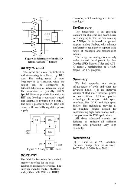
doutpd<strong>in</strong>pd<strong>in</strong>ndoutnsenbobuflvdsoobufienblvdsoensenbienb-lvdsi+-lvdsi+lvdsienlvdsienFigure 2: Schematic of multi-IOcell <strong>in</strong> <strong>RadSafe</strong> TM libraryAll digital DLLsThe need for clock multiplicationand de-skew<strong>in</strong>g is achieved by DLLcore. The tun<strong>in</strong>g range of <strong>in</strong>putfrequency is 25÷125MHz, while theoutput can be configured to1X/2X/4X/bypass of reference <strong>in</strong>put.The resolution is typically