Stress and Diffusion Resistance of Low Temperature ... - Sematech
Stress and Diffusion Resistance of Low Temperature ... - Sematech
Stress and Diffusion Resistance of Low Temperature ... - Sematech
- No tags were found...
You also want an ePaper? Increase the reach of your titles
YUMPU automatically turns print PDFs into web optimized ePapers that Google loves.
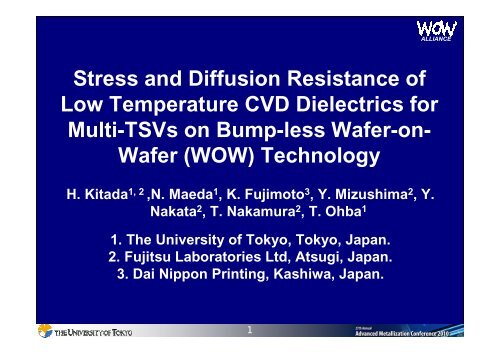
ALLIANCE<strong>Stress</strong> <strong>and</strong> <strong>Diffusion</strong> <strong>Resistance</strong> <strong>of</strong><strong>Low</strong> <strong>Temperature</strong> CVD Dielectrics forMulti-TSVs on Bump-less Wafer-on-Wafer (WOW) TechnologyH. Kitada 1, 2 ,N. Maeda 1 , K. Fujimoto 3 , Y. Mizushima 2 , Y.Nakata 2 , T. Nakamura 2 , T. Ohba 11. The University <strong>of</strong> Tokyo, Tokyo, Japan.2. Fujitsu Laboratories Ltd, Atsugi, Japan.3. Dai Nippon Printing, Kashiwa, Japan.1
Cu TSV process in Bump less WOW processALLIANCE1) Wafer level bonding2) TSV PR & Si DRIE3) PECVDSi #2M2 RDL TrenchPRTSV HoleSiN(This work)AdhesiveM1 RDLSi #14) SiN Self-alignEtchingPECVD-SINSi #2Si #15) PVD metal barrier& Copper ECDECD-CopperTi LinerSi #2Si #16) PlanarizationM2 RDLSi #2Si #2Si #2TSVM1 RDLSi #1Si #1Si #1‣ The temperature less than 200 deg C is needed due to usingorganic bonding materials in our TSV process.4
Advantage <strong>of</strong> Bump-less technologyALLIANCE1000Trend <strong>of</strong> Bump pitch <strong>and</strong> heightFBGAHeight (µm)10010WOW-TSVµ-BUMPThis work
Advantage <strong>of</strong> Bump-less technology Cont’d<strong>Resistance</strong> (Ohm/pin)1.0E+011.0E+001.0E-011.0E-02TSV <strong>and</strong> Bump resistance1/30Res.WOW-TSV(FtoB)0 10 20 30 40Via diameter (µm)6µ-Bump(FtoF)12.3 timespins numberALLIANCE‣ The via resistance <strong>of</strong> Copper TSV is 10 times smaller than that <strong>of</strong> Lead freeBump connection, <strong>and</strong> It’s 12 times the number <strong>of</strong> pins are installed in thesame chip area.
Advantage <strong>of</strong> Bump-less technology Cont’d<strong>Stress</strong> (MPa)8006004002000-200Adhesive thickness dependenceWOWBump-lessYield stress (Cu 30umT)(a) Under TSV (Bulk)(c) Cu/<strong>Low</strong>-k area(b) Side <strong>of</strong> TSV0 10 20Adhesive thickness (µm)7µ Bump3 stacked TSV structure(a) (c)Via diameter : 30µmAdhesive CTE : 40ppmSi thickness : 40µmALLIANCE‣ Residual stress on the <strong>Low</strong>-k/Cu layer at underneath <strong>of</strong> TSV isbigger than the another region <strong>of</strong> around TSV.(b)T ad.Kitada. et. al. IITC2009
Cu thermal diffusion in PECVD Si(O)N filmsALLIANCECu concentration (atms/cm 3 )1.0E+231.0E+211.0E+191.0E+17CuSiOND/D 0 =0.601.0E+150 200 400Si400 deg C x 10h agingD/D 0 =0.63D/D 0 =0.65Depth (nm)9Deposited CuSiNSiSIMSBack grinding tonear the interface‣ Cu diffusion pr<strong>of</strong>ile is measured using backside SIMS.
Cu diffusion depth into SiON filmALLIANCEThickness <strong>of</strong> Si(O)N (t: nm)100001000100101Si(O)N/Si TSVCuLT SiON (low dense)CuLT SiON (high dense)HT SiN10 15 atms/cm 310 10 atms/cm 3LT = <strong>Low</strong> <strong>Temperature</strong> PECVD (~150 ˚C)HT = High <strong>Temperature</strong> PECVD (~350 ˚C)0.2 0.4 0.6 0.8 1.0Relative Density <strong>of</strong> Si(O)N10after 400 ˚C/10hr agingatms/cm 3t10 2210 1510 10CuSi(O)NDiffused Cu‣ Critical thickness <strong>of</strong> SiON films has been defined to obtainenough thickness for preventing Cu diffusion.Si
Comparison <strong>of</strong> leakage currentALLIANCECurrent (A/cm 2 )1.0E-031.0E-061.0E-091.0E-12Deposition : 150 deg CSiO 2 D/D 0 =0.63SiON(3)D/D 0 =0.59SiON(4)D/D 0 =0.630 2 4E (MV/cm)‣ Leakage current is varied with density <strong>of</strong> SiON film.11
Multi-TSV structure in bump-less TSVALLIANCEFIB-SEM image <strong>of</strong> Bird's-eye viewCu-Multiple TSV12µm10µmBEOLSi(2)AdhesiveSi(1)10µm‣ Multiple TSV design using small via is provided with lower stress,lower via resistance <strong>and</strong> multi-functionally.12
Leakage current between TSVs blocksALLIANCE1.0E-06I (A)1.0E-1040µm1.0E-140 1 2 3 4 5V (V)‣ The low temperature SiON film with controlled propertiessatisfy leakage current performance.13
Yield <strong>of</strong> BEOL interconnects with TSVALLIANCEProbability (%)99.9999.9999050101.1.0131k Sparse ChainWith TSVW/o TSV251k Dense ChainW/o TSVWith TSV0 4E10 4 8E10 4 1.2E10 5<strong>Resistance</strong> (Ohm)14BEOL: W0.4µm Dense Chain+ TSV: 10µm Multi-ViaW/o TSVWith TSV0.21mOhm/blocks‣ There is no open failure <strong>and</strong> the resistance changes are smallenough.
Thermal cycle testing resultALLIANCEw/oTSV processwithTSV processAfterTC 1000cycle0.4µm dense chain (Ω)1.04E+051.00E+051.01E+053µm single line(Ω)10.02 10.04 9.97Thermal cycle testing: -55 to 125 deg C, 1000 cyclesBEOL resistance connected with TSV0.4um densechain3um singleLine‣ No resistance change was observed both BEOL interconnectbetween before TSV process <strong>and</strong> after TC testing.15
Example <strong>of</strong> residual stress distributionALLIANCECompressiveTensileSi200MPa-600 -400 -200 0 200 400 600 900(Mpa)BEOLSi100 µmCu525MPaCu(16.6ppm)SiNSi(2.3ppm)Adhesive (52ppm)BEOLSi sub.BEOL Cu/<strong>Low</strong>-k-100MPa900MPaSi sub.Kitada. et. al. IITC2009‣ Tensile stress at Cu/<strong>Low</strong>-k area was generated due to compressivestress occurred underneath <strong>of</strong> TSVs during TSV process.16
Cu-TSV deformation as a function <strong>of</strong> temperatureALLIANCEHeight (µm)0.40-0.4This work100-µmφ50-µmφ10-µmφConventionalPumping heightSiO2SiCu-0.80 200 400 600<strong>Temperature</strong> (deg C)‣ Pumping volume at the dielectric films on TSV is decreasing withsmaller via diameter <strong>and</strong> lower process temperature variation.17
SummaryALLIANCEWe demonstrated LT-PECVD SiON technology can usefor high yield <strong>and</strong> reliability via structure by the WOW’sbump-less TSV process.1. FEM simulation existed low temperature process isvery important for thermal stress near the Cu-TSV.2. Copper thermal diffusion <strong>and</strong> leakage current dependon LT-PECVD film density.3. For TSV process, lower leakage current, highbreakdown voltage, lower contact resistance <strong>and</strong> noresistance change after TC testing were realized byLT-PECVD SiON with film properties; D/D 0 <strong>of</strong> 0.63formed at 150 deg C.18
AcknowledgeALLIANCEALLIANCEThis work is carried out at 3D development program in the WOWalliance <strong>and</strong> the WOW Research Center Corporation.We would like to thank DISCO Corporation, Nissan Chemical,FEI Company, <strong>and</strong> Fujitsu semiconductor for wafer thinning,bonding, high throughput dual beam FIB-SEM samplepreparation, <strong>and</strong> device wafer preparation.19
Cu diffusion rate as a function <strong>of</strong> density <strong>of</strong> SiNALLIANCECu diffusion rate (cm 2 /s)1.E-081.E-091.E-10SiO 2SiON400 deg C x 10h aging<strong>Low</strong>1.E-110.2 0.6 1.0Relative density <strong>of</strong> SiON‣ The film with lower density shows higher diffusion rate.20NitrideratioHighKitada. et. al. IITC2010


