Reliability Studies of SnAgCu BGA Solder Joints on Ni/Cu/Au ...
Reliability Studies of SnAgCu BGA Solder Joints on Ni/Cu/Au ...
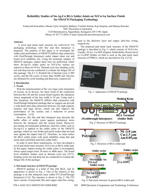
Reliability Studies of SnAgCu BGA Solder Joints on Ni/Cu/Au ...
- No tags were found...

Create successful ePaper yourself
Turn your PDF publications into a flip-book with our unique Google optimized e-Paper software.
II. Experimental procedures1. Prototype designThe prototype design and specificati<strong>on</strong>s are shown inTable 1. The logic-TEG chips have 400 electrodes for interchipc<strong>on</strong>necti<strong>on</strong>s with a 50 µm pitch in an area array at thecenter <str<strong>on</strong>g>of</str<strong>on</strong>g> each chip and 500 external electrodes with a 35 µmpitch with a staggered layout at the periphery <str<strong>on</strong>g>of</str<strong>on</strong>g> the chip. Thememory-TEG chips have 400 electrodes for inter-chipc<strong>on</strong>necti<strong>on</strong>s corresp<strong>on</strong>ding to the logic electrode layout. Twochips are encapsulated in a fine-pitch <str<strong>on</strong>g>BGA</str<strong>on</strong>g> type package thatmeasures 15 mm × 15 mm and 500 solder balls with a 0.5 mmpitch next to the logic chip. The thickness <str<strong>on</strong>g>of</str<strong>on</strong>g> <strong>Ni</strong>, <strong>Cu</strong> and <strong>Au</strong>is 3.0, 1.5 and 0.05 µm, respectively. 0.300 mm solder ballswere attached to solder pads. The total thickness <str<strong>on</strong>g>of</str<strong>on</strong>g> thepackage including the solder balls is less than 1.0 mm. Thisprototype <str<strong>on</strong>g>of</str<strong>on</strong>g> SMAFTI package and system board wasdesigned to form daisy chain, by which the resistance <str<strong>on</strong>g>of</str<strong>on</strong>g> acomplete circuit can be m<strong>on</strong>itored and recorded.2. Fabricati<strong>on</strong> <str<strong>on</strong>g>of</str<strong>on</strong>g> the prototype <str<strong>on</strong>g>of</str<strong>on</strong>g> SMAFTI packageThe process flow is shown in Fig. 5; a photosensitivepolyimide layer was deposited <strong>on</strong> a support substrate, and<str<strong>on</strong>g>BGA</str<strong>on</strong>g> pad vias were patterned using photolithography process,in which <strong>Cu</strong>/<strong>Ni</strong> <str<strong>on</strong>g>BGA</str<strong>on</strong>g> pad layer was filled. The memory-TEGchips with Sn-Ag electroplated bumps were aligned andb<strong>on</strong>ded to the FTI formed substrate using a flip chip b<strong>on</strong>der.After reflowing, epoxy based underfill resin which wasdefined as “1 st level underfill resin”, was injected into the gapusing the capillary flow effect, and this resin was cured in anoven. A compressi<strong>on</strong> molding process was carried out for theFTI formed silic<strong>on</strong> wafer. An epoxy based moldingcompound with silica filler was used to encapsulate thememory-TEG chips and FTI surface. After removal <str<strong>on</strong>g>of</str<strong>on</strong>g> thesupport substrate, the surface <str<strong>on</strong>g>of</str<strong>on</strong>g> <strong>Cu</strong> layer appeared andelectoroless <strong>Au</strong> was plated <strong>on</strong> the exposed <strong>Cu</strong> layer. Thelogic-TEG chips with bumps were aligned and b<strong>on</strong>ded to theFTI. The same type <str<strong>on</strong>g>of</str<strong>on</strong>g> underfill resin used memory-TEGc<strong>on</strong>necti<strong>on</strong> was injected under the logic-TEG chips and cured.Table 1: Specificati<strong>on</strong>s <str<strong>on</strong>g>of</str<strong>on</strong>g> the prototype <str<strong>on</strong>g>of</str<strong>on</strong>g> SMAFTI packageDie sizeLogic 5.31 mm x 5.31 mmMemory 7.35 mm x 12.7 mmInter-chip50 µm (area array)c<strong>on</strong>necti<strong>on</strong>400 pinExternal electrode 35µm staggered (peripheral)<strong>on</strong> logic-TEG500 pinPackage typeFine pitch <str<strong>on</strong>g>BGA</str<strong>on</strong>g>Package size15 mm x 15 mm1 st levelunderfill resinType: A, Type: BPin500 pinPitch0.50 mm<str<strong>on</strong>g>BGA</str<strong>on</strong>g> solder SizeΦ0.300 mmjoints Compositi<strong>on</strong> Sn-3.0Ag-0.5<strong>Cu</strong>FluxWater solubleType: A, Type: BFig. 5: Fabricati<strong>on</strong> process flowFig. 6: Reflow c<strong>on</strong>diti<strong>on</strong> for solder ball attachmentFig. 7: Appearance <str<strong>on</strong>g>of</str<strong>on</strong>g> SMAFTI resin wafer with solder ballsWater soluble flux was printed by screen printer <strong>on</strong> the<strong>Ni</strong>/<strong>Cu</strong>/<strong>Au</strong> <str<strong>on</strong>g>BGA</str<strong>on</strong>g> pad, and Sn-Ag-<strong>Cu</strong> solder balls were attachedby wafer level solder ball mounter (Athlete FA BM-1000). Amodified screen printing mask was used to place the solderball <strong>on</strong> the pad. 42,604 balls were attached at <strong>on</strong>e time. Thenthe resin wafer was reflowed in a 7-z<strong>on</strong>e reflow gas-forcedc<strong>on</strong>vecti<strong>on</strong>oven. During reflowing, nitrogen was provided inthe oven to keep the c<strong>on</strong>centrati<strong>on</strong> <str<strong>on</strong>g>of</str<strong>on</strong>g> oxygen less than 100ppm. As shown in Fig. 6, reflow peak temperature was 240 ℃and dwell time over 220 ℃ was 58 sec<strong>on</strong>d. The rate <str<strong>on</strong>g>of</str<strong>on</strong>g>284 2008 Electr<strong>on</strong>ic Comp<strong>on</strong>ents and Technology C<strong>on</strong>ference
defects such as missing balls was 170 ppm. The appearance <str<strong>on</strong>g>of</str<strong>on</strong>g>SMAFTI resin wafer with solder balls attached is shown inFig. 7. Water soluble flux was cleaned by de-i<strong>on</strong>ized waterwhile the resin wafer was cut into the single pieces by theautomatic dicing saw.3. Board level assembly and reliability testBefore board level assembly, SMAFTI packages wereaged at 125 ℃ for 10 hours, and stored at 30 ℃/ 70 % for 168hours. Then they were mounted <strong>on</strong> FR-4 printed circuit boardafter printing <str<strong>on</strong>g>of</str<strong>on</strong>g> no-clean Sn-Ag-<strong>Cu</strong> solder paste and werereflowed twice in a 12-z<strong>on</strong>e c<strong>on</strong>vecti<strong>on</strong> oven. As shown inFig. 8, reflow peak temperature was 250 ℃ and dwell timeover 220 ℃ was 46 sec<strong>on</strong>d. After reflowing, epoxy basedunderfill resin that was defined as “2 nd level underfill resin”was injected between SMAFTI package printed circuit board,and cured in an oven.Board level reliability tests such as thermal cyclic test(TCT), cyclic bending test, and drop test were performed. Inorder to obtain the fatigue life <str<strong>on</strong>g>of</str<strong>on</strong>g> the solder joints, SMAFTIpackage and the printed circuit board were designed to formdaisy chain, by which the resistance <str<strong>on</strong>g>of</str<strong>on</strong>g> a complete circuit canbe m<strong>on</strong>itored and recorded.TCT temperature ranged from -40 °C to 125 °C, and both<str<strong>on</strong>g>of</str<strong>on</strong>g> the soak time at -40 ℃and 125 °C were 10 minuets. Bothramp up and ramp down rates were about 15 °C /min. Thecyclic bending test was under the c<strong>on</strong>diti<strong>on</strong> <str<strong>on</strong>g>of</str<strong>on</strong>g> 20 mmdeflecti<strong>on</strong>and 1 sec<strong>on</strong>d /cycle frequency. Drop height used inthis test was 1,000 mm.Table 2: Board level assembly c<strong>on</strong>diti<strong>on</strong>LayerFR-4 6layerSystemPad structure<strong>Cu</strong> OSP/ N<strong>on</strong> soldermask definedboardSize 40mm x 110 mmThicknesst = 1.00 mm<str<strong>on</strong>g>Solder</str<strong>on</strong>g> paste<str<strong>on</strong>g>SnAg<strong>Cu</strong></str<strong>on</strong>g> (no-clean)t = 0.12 mmPre c<strong>on</strong>diti<strong>on</strong> 125 0 C/10h+30 0 C/70%RH/168h2 nd levelunderfill resinType:A,Type:BIII. Results and discussi<strong>on</strong>Fig. 9: SEM image <str<strong>on</strong>g>of</str<strong>on</strong>g> <str<strong>on</strong>g>BGA</str<strong>on</strong>g> ball joint (×300)<strong>Cu</strong>Sn<strong>Au</strong>AgFig. 10: EPMA image <str<strong>on</strong>g>of</str<strong>on</strong>g> <str<strong>on</strong>g>BGA</str<strong>on</strong>g> ball joint (×300)No.3 <str<strong>on</strong>g>Solder</str<strong>on</strong>g>No.2 (<strong>Cu</strong>,<strong>Ni</strong>) 6Sn 5No.1 <strong>Cu</strong> 6Sn 5Fig. 8: Reflow c<strong>on</strong>diti<strong>on</strong> for board level assembly2µmNo.4 <strong>Ni</strong> layerFig. 11: SEM image <str<strong>on</strong>g>of</str<strong>on</strong>g> IMC layer (×5000)285 2008 Electr<strong>on</strong>ic Comp<strong>on</strong>ents and Technology C<strong>on</strong>ference
<strong>Cu</strong> Sn No.1 <strong>Ni</strong>,<strong>Cu</strong>SnNo.3Fig. 12: Results <str<strong>on</strong>g>of</str<strong>on</strong>g> EDX analysis (×5000)No.2No.41. Cross secti<strong>on</strong> <str<strong>on</strong>g>of</str<strong>on</strong>g> solder jointsCross secti<strong>on</strong>ing analysis was performed <strong>on</strong> the solderjoint <str<strong>on</strong>g>of</str<strong>on</strong>g> SMAFTI package. Sn-Ag-<strong>Cu</strong> solder was attached <strong>on</strong>the <strong>Ni</strong>/<strong>Cu</strong>/<strong>Au</strong> pad shown in Fig. 3. Fig. 9 shows a SEM image<str<strong>on</strong>g>of</str<strong>on</strong>g> a cross-secti<strong>on</strong> <str<strong>on</strong>g>of</str<strong>on</strong>g> a <str<strong>on</strong>g>BGA</str<strong>on</strong>g> solder joint <str<strong>on</strong>g>of</str<strong>on</strong>g> SMAFTI packageafter fabricati<strong>on</strong>. The distributi<strong>on</strong>s <str<strong>on</strong>g>of</str<strong>on</strong>g> <strong>Cu</strong>, Sn, <strong>Au</strong> and Agobserved by EPMA can be seen in Fig. 10. The SEM image<str<strong>on</strong>g>of</str<strong>on</strong>g> IMC (Intermetallic compound) layer is shown in Fig. 11,whose EDX analysis results are described in Fig. 12.There was <strong>on</strong>ly <strong>Ni</strong> detected as shown in No.4 <str<strong>on</strong>g>of</str<strong>on</strong>g> Fig. 12, sothis layer in No.4 <str<strong>on</strong>g>of</str<strong>on</strong>g> Fig. 11 was the <strong>Ni</strong> layer <str<strong>on</strong>g>of</str<strong>on</strong>g> the <strong>Ni</strong>/<strong>Cu</strong>/<strong>Au</strong>pad. There was <strong>on</strong>ly Sn detected as shown in Fig. 12, whichshowed No.3 in Fig. 11to be the solder.During reflowing, almost all <strong>Au</strong> whose thickness was 0.5µm was dissolved into the solder uniformly as shown in Fig.10. The thickness <str<strong>on</strong>g>of</str<strong>on</strong>g> <strong>Cu</strong> layer was about1.5 µm, and wasc<strong>on</strong>sumed entirely to form <strong>Cu</strong> 6 Sn 5 layer, whose meanthickness became 2.1µm after reflowing. And there was no <strong>Ni</strong>or <strong>Au</strong> detected in this IMC layer as shown in No.1 <str<strong>on</strong>g>of</str<strong>on</strong>g> Fig. 12.There was another IMC layer between <strong>Cu</strong> 6 Sn 5 and <strong>Ni</strong>layer, which c<strong>on</strong>sisted <str<strong>on</strong>g>of</str<strong>on</strong>g> <strong>Cu</strong>, <strong>Ni</strong> and Sn as shown in No.2 <str<strong>on</strong>g>of</str<strong>on</strong>g>Fig .12. During reflowing, after the c<strong>on</strong>sumpti<strong>on</strong> <str<strong>on</strong>g>of</str<strong>on</strong>g> <strong>Au</strong> and<strong>Cu</strong>, <strong>Ni</strong> layer below <strong>Cu</strong> formed thin (<strong>Cu</strong>,<strong>Ni</strong>) 6 Sn 5 layer[8,10,11]. Since <strong>Cu</strong> layer was situated between solder and <strong>Ni</strong>,this layer decreased the degradati<strong>on</strong> <str<strong>on</strong>g>of</str<strong>on</strong>g> <strong>Ni</strong> layer during liquidphase reacti<strong>on</strong> with the solder.When the Sn-Ag-<strong>Cu</strong> solder is attached <strong>on</strong> the <strong>Ni</strong>/<strong>Au</strong> padas shown in Fig. 4, (<strong>Cu</strong>,<strong>Ni</strong>,<strong>Au</strong>) 6 Sn 5 forms as IMC layer.When the solder is attached <strong>on</strong> the <strong>Cu</strong>-OSP or the <strong>Cu</strong>-SOPpad, <strong>Cu</strong> 6 Sn 5 forms. In this study, the IMC layer between theSn-Ag-<strong>Cu</strong> solder and the <strong>Ni</strong>/<strong>Cu</strong>/<strong>Au</strong> pad was investigated, andfound to be form <strong>Cu</strong> 6 Sn 5 and thin (<strong>Cu</strong>,<strong>Ni</strong>) 6 Sn 5 .2. The results <str<strong>on</strong>g>of</str<strong>on</strong>g> impact shear studyThe solder joint integrity <str<strong>on</strong>g>of</str<strong>on</strong>g> SMAFTI against impact loadwas investigated by way <str<strong>on</strong>g>of</str<strong>on</strong>g> the impact shear testing. Theresults were compared with those <str<strong>on</strong>g>of</str<strong>on</strong>g> FP<str<strong>on</strong>g>BGA</str<strong>on</strong>g> whose pad metalstructure was <strong>Ni</strong>/<strong>Au</strong>, <strong>Cu</strong>-OSP and <strong>Cu</strong>-SOP. At the shearspeed <str<strong>on</strong>g>of</str<strong>on</strong>g> 0.1 mm/s, the b<strong>on</strong>d tester (Dage Series 4000) wasused, and the impact shear tester (Dage 4000-HS) wasintroduced to quantify the solder joint integrity for impactload as shown in Fig. 13, whose test speed ranged from 10mm/s to 4000 mm/s [7]. Not <strong>on</strong>ly shear load but also solderjoint energy was plotted, and discussed which was superior topresent the solder joint integrity. 30 points <str<strong>on</strong>g>of</str<strong>on</strong>g> solder jointswith <strong>Ni</strong>/<strong>Au</strong> and <strong>Ni</strong>/<strong>Cu</strong>/<strong>Au</strong> pad were tested for impact shear<strong>Ni</strong>Snstudy in each c<strong>on</strong>diti<strong>on</strong>, while 20 points <str<strong>on</strong>g>of</str<strong>on</strong>g> solder joints with<strong>Cu</strong>-SOP and <strong>Cu</strong>-SOP pad were testedThe results <str<strong>on</strong>g>of</str<strong>on</strong>g> the impact shear load as a functi<strong>on</strong> <str<strong>on</strong>g>of</str<strong>on</strong>g> shearspeed are plotted in Fig. 14. The horiz<strong>on</strong>tal axis is the shearspeed that is showed in logarithm, and the vertical axis is theshear load. Although the test c<strong>on</strong>diti<strong>on</strong>s were the same am<strong>on</strong>gthe pad surface finishes, the plots in horiz<strong>on</strong>tal axis arestaggered intenti<strong>on</strong>ally so that they can be seen clearly. Thetop <str<strong>on</strong>g>of</str<strong>on</strong>g> the error bar means the maximum value, while thebottom means the minimum.The shear strength change <str<strong>on</strong>g>of</str<strong>on</strong>g> solder joints with <strong>Ni</strong>/<strong>Au</strong>against the shear speed was different from those with <strong>Cu</strong>-OSP, <strong>Cu</strong>-SOP and <strong>Ni</strong>/<strong>Cu</strong>/<strong>Au</strong>. The mean strengths <str<strong>on</strong>g>of</str<strong>on</strong>g> solderjoints with <strong>Ni</strong>/<strong>Au</strong> were about 4 N at all speeds, while thehigher the shear rate became, the higher the shear strengthwith <strong>Cu</strong>-OSP, <strong>Cu</strong>-SOP and <strong>Ni</strong>/<strong>Cu</strong>/<strong>Au</strong> grew. The defecti<strong>on</strong> <str<strong>on</strong>g>of</str<strong>on</strong>g>shear strength with <strong>Ni</strong>/<strong>Au</strong> was the largest <str<strong>on</strong>g>of</str<strong>on</strong>g> all <str<strong>on</strong>g>of</str<strong>on</strong>g> these padmetal surface finishes, and the minimum shear strength with<strong>Ni</strong>/<strong>Au</strong> was the weakest <str<strong>on</strong>g>of</str<strong>on</strong>g> all at the speed <str<strong>on</strong>g>of</str<strong>on</strong>g> 10 mm/s and100mm/s. On the other hand, although the mean shear loadswith <strong>Ni</strong>/<strong>Cu</strong>/<strong>Au</strong> seemed to be lower than those <str<strong>on</strong>g>of</str<strong>on</strong>g> the otherpads, the deflecti<strong>on</strong>s were the smallest <str<strong>on</strong>g>of</str<strong>on</strong>g> all, which indicatesthat solder joints with <strong>Ni</strong>/<strong>Cu</strong>/<strong>Au</strong> have good durability againstimpact loads.The changes <str<strong>on</strong>g>of</str<strong>on</strong>g> the solder joint energy against the shearspeed are plotted in Fig. 15, where the horiz<strong>on</strong>tal axis is theshear speed showed in logarithm, and the vertical axis is theshear load. The plots in horiz<strong>on</strong>tal axis are staggered, too.As the shear speed grew faster, the solder joint energieswith <strong>Ni</strong>/<strong>Au</strong>, <strong>Cu</strong>-SOP and <strong>Cu</strong>-SOP decreased gradually. Andthe solder joint energies with <strong>Ni</strong>/<strong>Cu</strong>/<strong>Au</strong> showed the sameinclinati<strong>on</strong>s as the others. On the whole, the mean solder jointenergies with <strong>Ni</strong>/<strong>Au</strong> seemed to be the smallest <str<strong>on</strong>g>of</str<strong>on</strong>g> all.However, the defecti<strong>on</strong>s were the smallest and the minimumsolder joint energies seemed to be the highest <str<strong>on</strong>g>of</str<strong>on</strong>g> all the padmetal surface finishes, which indicates the solder joints with<strong>Ni</strong>/<strong>Cu</strong>/<strong>Au</strong> have good durability against impact loads.From the results shown in Fig. 14 and Fig. 15, it seems thatthe solder joints with <strong>Cu</strong> 6 Sn 5 IMC layer have better jointreliabilities against the impact load than those with(<strong>Cu</strong>,<strong>Ni</strong>,<strong>Au</strong>) 6 Sn 5 . It indicates that the c<strong>on</strong>centrati<strong>on</strong> <str<strong>on</strong>g>of</str<strong>on</strong>g> <strong>Cu</strong> thatdiffuses into the solder changes the hardness <str<strong>on</strong>g>of</str<strong>on</strong>g> the solderbulk, and the solder joint integrity <str<strong>on</strong>g>of</str<strong>on</strong>g> IMC layer is better thanthat <str<strong>on</strong>g>of</str<strong>on</strong>g> (<strong>Cu</strong>,<strong>Ni</strong>,<strong>Au</strong>) 6 Sn 5 . And the small amount <str<strong>on</strong>g>of</str<strong>on</strong>g> <strong>Au</strong> into thesolder may change the solder joint integrity <str<strong>on</strong>g>of</str<strong>on</strong>g> <strong>Ni</strong>/<strong>Cu</strong>/<strong>Au</strong>better than <strong>Cu</strong>-OSP and <strong>Cu</strong>-SOP.The relati<strong>on</strong>ship between the shear load and the solder jointenergy is c<strong>on</strong>sidered and described in Fig. 16, where thehoriz<strong>on</strong>tal axis is the displacement <str<strong>on</strong>g>of</str<strong>on</strong>g> the shear tool, and thevertical axis is the shear load. F bulk and F interfacial is defined asthe shear loads <str<strong>on</strong>g>of</str<strong>on</strong>g> bulk solder failure mode and interfacialfailure mode, respectively. E bulk and E interfacial are defined asthe solder joint energies which were the integrals <str<strong>on</strong>g>of</str<strong>on</strong>g> shearload at the length, l.E = ∫F(l) dl286 2008 Electr<strong>on</strong>ic Comp<strong>on</strong>ents and Technology C<strong>on</strong>ference
In Fig. 16, F interfacial is as high as F bulk , while E interfacial ismuch smaller than E bulk . It indicates that solder joint energycan describe the solder joint integrity more clearly than shearload.15F interfacialF bulkHeight:50µmShear Speed:10 – 4000mm/sDisplacementImpact shear load [N]105E interfacialF(l):Shearload at lFig. 13: The image <str<strong>on</strong>g>of</str<strong>on</strong>g> impact shear testingE bulkShear Load [N]<str<strong>on</strong>g>Solder</str<strong>on</strong>g> Joint Energy [mJ]8765432102.52.01.51.00.50.1mm/s10mm/s100mm/s1000mm/s<strong>Ni</strong>/<strong>Au</strong><strong>Cu</strong>-OSP<strong>Cu</strong>-SOP<strong>Ni</strong>/<strong>Cu</strong>/<strong>Au</strong>10 -1 10 0 10 1 10 2 10 3 10 4Shear Speed [mm/s]Fig. 14: Shear load versus shear speed<strong>Ni</strong>/<strong>Au</strong><strong>Cu</strong>-OSP<strong>Cu</strong>-SOP4000mm/s<strong>Ni</strong>/<strong>Cu</strong>/<strong>Au</strong>10 mm/s 100 mm/s 1000 mm/s 4000 mm/s0.010 1 10 2 10 3 10 4Shear Speed [mm/s]Fig. 15: <str<strong>on</strong>g>Solder</str<strong>on</strong>g> joint energy versus shear speed00 200 400 l600 800 1000 1200Displacement <str<strong>on</strong>g>of</str<strong>on</strong>g> the shear tool [um]Fig. 16: The relati<strong>on</strong>ship between shear loadand solder joint energy3. Thermal warpage and solder surface c<strong>on</strong>diti<strong>on</strong><str<strong>on</strong>g>BGA</str<strong>on</strong>g> type package sometimes causes de-wetting issue <str<strong>on</strong>g>of</str<strong>on</strong>g>solder joints at board level assembly process. There are someroot causes <str<strong>on</strong>g>of</str<strong>on</strong>g> this failure induced by the design <str<strong>on</strong>g>of</str<strong>on</strong>g> thepackage. One is the thermal warpage change <str<strong>on</strong>g>of</str<strong>on</strong>g> <str<strong>on</strong>g>BGA</str<strong>on</strong>g> packageduring reflowing. Another <strong>on</strong>e is the oxidati<strong>on</strong> or thepolluti<strong>on</strong> <str<strong>on</strong>g>of</str<strong>on</strong>g> solder ball surface [12]. In order to care thisfailure, thermal warpage and solder surface c<strong>on</strong>diti<strong>on</strong> wereevaluated.As SMAFTI package shown in Fig. 2 c<strong>on</strong>sists <str<strong>on</strong>g>of</str<strong>on</strong>g> Si dice,molded resin, and very thin FTI layer, the main factor thatrules the warpage is the thermal characteristic caused by thesematerials. Fig. 17 shows the thermal warpage change againstthe temperature <str<strong>on</strong>g>of</str<strong>on</strong>g> SMAFTI package, which was measuredusing Shadow moiré method. According to the result, thewarpage change during reflowing was less than 20 µm, andthe maximum warpage was 47µm, which are small enoughcompared with the height <str<strong>on</strong>g>of</str<strong>on</strong>g> solder ball. Higher volume <str<strong>on</strong>g>of</str<strong>on</strong>g> theSi and lower volumes <str<strong>on</strong>g>of</str<strong>on</strong>g> interposer and molded resin thanthose <str<strong>on</strong>g>of</str<strong>on</strong>g> standard FP<str<strong>on</strong>g>BGA</str<strong>on</strong>g> seems to make the warpage smaller.245 0 CTemperature [K]38 0 C160 0 C29μm220 0 CDefiniti<strong>on</strong> <str<strong>on</strong>g>of</str<strong>on</strong>g> warpage41μm60 0 C47μm40μm47μmReflow time [s]Fig. 17: Thermal warpage change <str<strong>on</strong>g>of</str<strong>on</strong>g> SMAFTI package-+287 2008 Electr<strong>on</strong>ic Comp<strong>on</strong>ents and Technology C<strong>on</strong>ference
Relative C<strong>on</strong>centrati<strong>on</strong> [%]Thickness <str<strong>on</strong>g>of</str<strong>on</strong>g> Oxidati<strong>on</strong> Layer [nm]CPeak <str<strong>on</strong>g>of</str<strong>on</strong>g> OOSnThickness <str<strong>on</strong>g>of</str<strong>on</strong>g> Oxidizati<strong>on</strong> Layer½peak <str<strong>on</strong>g>of</str<strong>on</strong>g> OSputtering Time [min]Fig. 18: Depth pr<str<strong>on</strong>g>of</str<strong>on</strong>g>ile <str<strong>on</strong>g>of</str<strong>on</strong>g> <strong>Au</strong>ger electr<strong>on</strong> microscopy15105Flux AFlux BN = 3 points00 48 96 144 192 240 288 336Exposure Time at 30 o /70%RH [h]Fig. 19: Thickness change <str<strong>on</strong>g>of</str<strong>on</strong>g> oxidati<strong>on</strong> layer at 30°C /70 %2. Board level reliability testAs menti<strong>on</strong>ed in previous secti<strong>on</strong>, 1 st level underfill resintype “a” and “b” were used to encapsulate flip chip solderjoints in the SMAFTI package. Another underfill resin type“A” and “B” were used to encapsulate the <str<strong>on</strong>g>BGA</str<strong>on</strong>g> solder jointsbetween the package and the printed circuit board. Wedefined this underfill resin as “2 nd level underfill resin”.Therefore, there were 4 types <str<strong>on</strong>g>of</str<strong>on</strong>g> specimens evaluated in thisstudy changing underfill resins. The results <str<strong>on</strong>g>of</str<strong>on</strong>g> the board levelreliability test are shown in Table 3.The results <str<strong>on</strong>g>of</str<strong>on</strong>g> thermal cyclic test are described in Fig. 19.For the test vehicle with 1 st level underfill resin “a”, and 2 ndlevel underfill resin “A”, the first failure occurred at 1006cycles, and 0.1 % Weibull life <str<strong>on</strong>g>of</str<strong>on</strong>g> thermal cycle was 296cycles. For the vehicle with 1 st level underfill resin “a” and 2 ndlevel underfill resin “B”, the first failure occurred at 955cycles, and 0.1% Weiblull life was 51 cycles. For the vehiclewith 1 st level underfill resin “b” and 2 nd level underfill resin“A”, the first failure and 0.1 % life was 931 and 306 cycles,respectively, while for the vehicle with 1 st level underfill resin“b” and 2 nd level underfill resin “B”, 1406 and 989 cycles,respectively. These results indicate that the material properties<str<strong>on</strong>g>of</str<strong>on</strong>g> both <str<strong>on</strong>g>of</str<strong>on</strong>g> 1 st level underfill resin and 2 nd level underfill resinare very important for thermal cycle reliability, and thatoptimized resins can ensure sufficient reliability for this newinterc<strong>on</strong>necti<strong>on</strong> technology.Table 3: Results <str<strong>on</strong>g>of</str<strong>on</strong>g> board level reliability test <str<strong>on</strong>g>of</str<strong>on</strong>g> SMAFTIUnderfillTCT Cyclic DropResin[cycle] Bending TestYield1 st 2 nd FirstTest (Min) (Min)Ffailure (0.1%) [cycle] [cycle]a A Initial 1006 296 >20000 >10a B failure 955 51 >20000 >10b A 0/108 931 306 >20000 >10b B pcs 1406 989 >20000 >10The surface <str<strong>on</strong>g>of</str<strong>on</strong>g> the solder balls were c<strong>on</strong>trolled by flux andwashing c<strong>on</strong>diti<strong>on</strong>. To prevent the solder surface polluti<strong>on</strong>,the water used in the washing machine was not recycled, butdrained directly.The water soluble flux was chosen to reduce the thickness<str<strong>on</strong>g>of</str<strong>on</strong>g> oxidati<strong>on</strong> layer. The informati<strong>on</strong> <str<strong>on</strong>g>of</str<strong>on</strong>g> the solder surface wasobtained by <strong>Au</strong>ger electr<strong>on</strong> microscope. Fig. 18 shows thedepth pr<str<strong>on</strong>g>of</str<strong>on</strong>g>ile <str<strong>on</strong>g>of</str<strong>on</strong>g> the solder surface, where the horiz<strong>on</strong>tal axisis the sputtering time and the vertical axis is the relativec<strong>on</strong>centrati<strong>on</strong> <str<strong>on</strong>g>of</str<strong>on</strong>g> each element. The sputtering rate c<strong>on</strong>vertedto SiO 2 was 11nm/min. As shown in Fig. 18, 1/2 peak methodwas applied to quantify the thickness <str<strong>on</strong>g>of</str<strong>on</strong>g> oxidati<strong>on</strong> layer. Theevaluati<strong>on</strong> result was described in Fig. 19, where thehoriz<strong>on</strong>tal axis is the exposure time c<strong>on</strong>diti<strong>on</strong>ed at 30 °C and70 %RH humidity in a humidity chamber. Using flux type: B,the thickness <str<strong>on</strong>g>of</str<strong>on</strong>g> oxidati<strong>on</strong> layer could be kept thinner, andthere was no initial failure during assembly, which is shownin Table 3.F(t)99%95%90%60%50%40%10%5%1%0.1%Weibull Plot1stUF:type"a"/2ndUF:type"A"1stUF:type"a"/2ndUF:type"B"1stUF:type"b"/2ndUF:type"A"1stUF:type"b"/2ndUF:type"B"1 10 100 1000 10000cycleFig. 20: Weibull distributi<strong>on</strong>s for temperature cycledcomp<strong>on</strong>ents288 2008 Electr<strong>on</strong>ic Comp<strong>on</strong>ents and Technology C<strong>on</strong>ference
OpenMemory-TEGLogic-TEGPackage SideBoard Side100µmFig. 21: Failure locati<strong>on</strong> and mode <str<strong>on</strong>g>of</str<strong>on</strong>g> solder jointsThe failure mode was a crack in solder joints. The locati<strong>on</strong><str<strong>on</strong>g>of</str<strong>on</strong>g> the solder joint failure is shown in Fig. 20, where the redpins in the Figure show the cracks. All <str<strong>on</strong>g>of</str<strong>on</strong>g> the cracks occurredwithin the area <str<strong>on</strong>g>of</str<strong>on</strong>g> memory-TEG. It is obvious that duringTCT test, solder joints under the memory chip have muchstress.The results <str<strong>on</strong>g>of</str<strong>on</strong>g> cyclic bending and drop tests were shown inTable 3. The minimum life <str<strong>on</strong>g>of</str<strong>on</strong>g> cyclic bending test and droptest were more than 20,000 cycle and 10 cycles, respectively,whatever the type <str<strong>on</strong>g>of</str<strong>on</strong>g> the underfill resin was used.Accordingly, if the suitable underfill resins are chosen, thefeasibility <str<strong>on</strong>g>of</str<strong>on</strong>g> the fundamental reliability <str<strong>on</strong>g>of</str<strong>on</strong>g> the structure issuccessfully dem<strong>on</strong>strated to meet producti<strong>on</strong> qualityrequirements.IV. C<strong>on</strong>clusi<strong>on</strong>sA novel <str<strong>on</strong>g>BGA</str<strong>on</strong>g> pad metal structure, <strong>Ni</strong>/<strong>Cu</strong>/<strong>Au</strong> for waferlevel3-D packaging technology, SMAFTI was proposed andits reliability was investigated.The IMC layer between the Sn-Ag-<strong>Cu</strong> solder ball and the<strong>Ni</strong>/<strong>Cu</strong>/<strong>Au</strong> pad formed <strong>Cu</strong> 6 Sn 5 and thin (<strong>Cu</strong>,<strong>Ni</strong>) 6 Sn 5 , where <strong>Au</strong>dissolved into the solder entirely.The solder joint integrity <str<strong>on</strong>g>of</str<strong>on</strong>g> SMAFTI against impact loadwas investigated by way <str<strong>on</strong>g>of</str<strong>on</strong>g> the impact shear testing. Theresults were compared with those <str<strong>on</strong>g>of</str<strong>on</strong>g> FP<str<strong>on</strong>g>BGA</str<strong>on</strong>g> whose pad metalstructure was <strong>Ni</strong>/<strong>Au</strong>, <strong>Cu</strong>-OSP and <strong>Cu</strong>-SOP. On the whole, thesolder joints with <strong>Ni</strong>/<strong>Cu</strong>/<strong>Au</strong> have good durability againstimpact loads.The warpage change during reflowing was less than 20µm, and the maximum warpage was 47µm, which are smallenough compared with the height <str<strong>on</strong>g>of</str<strong>on</strong>g> solder ball. Usingsuitable flux, the thickness <str<strong>on</strong>g>of</str<strong>on</strong>g> oxidati<strong>on</strong> layer could be keptthinner, and there was no initial failure during assembly.Board level reliability tests such as thermal cyclic test(TCT), bending cyclic test, and drop test were performed. The0.1 % Weibull life <str<strong>on</strong>g>of</str<strong>on</strong>g> thermal cycle was 989 cycles, and thelife cycles <str<strong>on</strong>g>of</str<strong>on</strong>g> more than 20,000 and 10cycles were obtainedfor cyclic bending and drop tests, respectively.AcknowledgmentsThe authors would like to thank Katsuyuki Abe, HajimeYanase, and Junko Yamaki who helped this study. Specialthanks to Yukihiko Kato and Yoshiharu Fujimori for supportin wafer level assembly.References1. Kurita, Y., Soejima, K., et al, “A Novel “SMAFTI”Package for Inter-Chip Wide-Band Data Transfer ”, Proc56 th Electr<strong>on</strong>ic Comp<strong>on</strong>ents and Technology C<strong>on</strong>f, pp.170-179.2. Kurita, Y., Soejima, K., et al, “A Novel “SMAFTI”Package for Inter-Chip Wide-Band Data Transfer ”, Proc57 th Electr<strong>on</strong>ic Comp<strong>on</strong>ents and Technology C<strong>on</strong>f, pp.821-829.3. Ezaki, T., K<strong>on</strong>do, K., et al, “A 160Gb/s Interface DesignC<strong>on</strong>figurati<strong>on</strong> for Multichip LSI,” Proc. <str<strong>on</strong>g>of</str<strong>on</strong>g> IEEEInternati<strong>on</strong>al Solid-State Circuits C<strong>on</strong>ference (ISSCC2004), San Francisco, CA, Feb. 2004, pp.140–141, Vol.1.4. Kurita, Y., Maeda, M., et al, “Development <str<strong>on</strong>g>of</str<strong>on</strong>g> COC(Chip-On-Chip) Interc<strong>on</strong>necti<strong>on</strong> Technology,” Proc. <str<strong>on</strong>g>of</str<strong>on</strong>g>12 th Micro Electr<strong>on</strong>ics Symposium (MES 2002), Osaka,Japan, Oct. 2002, pp. 51–54.5. Kurita, Y., Soejima, K., et al, “Development <str<strong>on</strong>g>of</str<strong>on</strong>g> High-Density Inter-Chip-C<strong>on</strong>necti<strong>on</strong> Structure Package,” Proc.<str<strong>on</strong>g>of</str<strong>on</strong>g> 15 th Micro Electr<strong>on</strong>ics Symposium (MES 2005), Osaka,Japan, Oct. 2005, pp. 189–192.6. Kawashiro, F., Kurita, Y., et al, “Development <str<strong>on</strong>g>of</str<strong>on</strong>g> <str<strong>on</strong>g>BGA</str<strong>on</strong>g>Attach Process with High Density SiP Technology“SMAFTI”,” 13 th Symposium <strong>on</strong> Micro jointing andAssembly Technology in Electr<strong>on</strong>ics (MATE 2007),Yokohama, Japan, Feb. 2007, pp. 49–54.7. Newman, K., “<str<strong>on</strong>g>BGA</str<strong>on</strong>g> Brittle Fracture – Alternative <str<strong>on</strong>g>Solder</str<strong>on</strong>g>Joint Integrity Test Methods”, Proc 55 th Electr<strong>on</strong>icComp<strong>on</strong>ents and Technology C<strong>on</strong>f, pp. 170-179.8. Zeng, K., and Tu, K. N., “Six cases <str<strong>on</strong>g>of</str<strong>on</strong>g> reliability study <str<strong>on</strong>g>of</str<strong>on</strong>g>Pb-free solder joints in electr<strong>on</strong>ic packaging technology,”Materials Science and Engineering, R38 (2002), pp.55-105.9. Amagai, M., Toyoda, Y., et al, “High Drop Test<str<strong>on</strong>g>Reliability</str<strong>on</strong>g> : Lead-free <str<strong>on</strong>g>Solder</str<strong>on</strong>g>s ”, Proc 54 th Electr<strong>on</strong>icComp<strong>on</strong>ents and Technology C<strong>on</strong>f, pp. 1304-1309.10. Snugovsky, L., Snugovsky, P., et al, “Phase equilibria inSn rich corner <str<strong>on</strong>g>of</str<strong>on</strong>g> <strong>Cu</strong>-<strong>Ni</strong>-Sn system,” Material science andtechnology, vol. 22, No. 8(2006), pp.899-90211. Jurenka, C., Kim, J.Y. et al., “Effect <str<strong>on</strong>g>of</str<strong>on</strong>g> the <strong>Cu</strong> Thickness<strong>on</strong> the Stability <str<strong>on</strong>g>of</str<strong>on</strong>g> a <strong>Ni</strong>/<strong>Cu</strong> Bilayer UBM <str<strong>on</strong>g>of</str<strong>on</strong>g> Lead FreeMicrobumps During Liquid and Solid State Aging”, 2005Electr<strong>on</strong>ic Comp<strong>on</strong>ents and Technology C<strong>on</strong>ference,pp.89-93.12. Grigoriev, A. et al, “Surface oxidati<strong>on</strong> <str<strong>on</strong>g>of</str<strong>on</strong>g> liquid Sn,”Surface Science , Vol. 575 (2005), pp.223-232289 2008 Electr<strong>on</strong>ic Comp<strong>on</strong>ents and Technology C<strong>on</strong>ference