Thermal Stress Analysis of a Flip-Chip Parallel VCSEL - ECA Digital ...
Thermal Stress Analysis of a Flip-Chip Parallel VCSEL - ECA Digital ...
Thermal Stress Analysis of a Flip-Chip Parallel VCSEL - ECA Digital ...

Create successful ePaper yourself
Turn your PDF publications into a flip-book with our unique Google optimized e-Paper software.
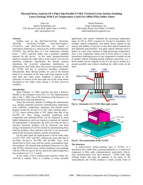
<strong>Thermal</strong> <strong>Stress</strong> <strong>Analysis</strong> Of A <strong>Flip</strong>-<strong>Chip</strong> <strong>Parallel</strong> <strong>VCSEL</strong> (Vertical-Cavity Surface-EmittingLaser) Package With Low-Temperature Lead-Free (48Sn-52In) Solder JointsJohn LauAgilent Technologies, Inc.5301 Stevens Creek Blvd, Santa Clara, CA 95052,john_lau@agilent.comWalter DauksherAvago Technologies, Inc.4380 Ziegler Road, Fort Collins, CO 80525,walter.dauksher@avagotech.comAbstractSolders such as the 48wt%Sn-52wt%In, 42wt%Sn-58wt%Bi, 63wt%Sn-37wt%Pb, Sn(3-4)wt%Ag(0.5-0.7)wt%Cu, and 80wt%Au-20wt%Sn, are studied asinterconnect materials in a vertical-cavity surface-emitting laser(<strong>VCSEL</strong>). The Sn52In alloy is a low temperature (meltingpoint = 118 o C) lead-free solder and a potential candidatematerial for this device. In this study, thermal-structuralanalysis evaluates the solder alloys in the context <strong>of</strong> in-serviceoperating conditions. Specifically, the thermal analysisdetermines the in-service temperature distributions, asinfluenced by each solder alloy, due to power generation withinthe <strong>VCSEL</strong> and due to convective boundary conditions.Subsequently, these thermal pr<strong>of</strong>iles are used as the thermalloads in an evaluation <strong>of</strong> the stress and creep response in thelaser pads and solder joints. Emphasis is placed on therelaxation <strong>of</strong> stresses at the laser pads and on the creep strainsdeveloped at the solder joints during a 24 hour power-oncondition.IntroductionSince February 13, 2003, lead-free has been a directive(RoHS) in the European Union (EU) [1]. The implementationdate is July 1, 2006. One <strong>of</strong> the intentions <strong>of</strong> the directive is toban lead and to find lead alternatives.Today the electronic industry is building the infrastructure(e.g., designs, materials, processes, manufacturing, inspections,tests, reliability, components, substrates, and printed circuitboards) around the Sn-Ag-Cu or SAC alloy (melting point ~217 o C), whose melting point is 34 o C higher than that <strong>of</strong> theSn37Pb [2]. Thus, during assembly (soldering), bothcomponents and substrates/PCBs will be subjected to muchhigher temperatures; and more expensive materials are requiredfor making them. Consequently, the total cost <strong>of</strong> the Sn-Ag-Culead-free electronic products will be increased, and moreenergy consumption [3] will be needed for manufacturing theselead-free products. Thus, lead-free with SAC is not necessarilygood for the electronics industry and the environment.On the other hand, the melting point <strong>of</strong> Sn-In solder alloyis 162 o C, 99 o C, 65 o C, and 20 o C, respectively, lower than that <strong>of</strong>Au-20Sn, Sn-Ag-Cu, Sn-37Pb, and Sn-58Bi. Thus, Sn-Inshould lead to lower costs and less energy consumptions leadfreeproducts. The thermal and mechanical behaviors <strong>of</strong> a flipchip<strong>VCSEL</strong> (Vertical-Cavity Surface-Emitting Laser) packagewith Sn-37Pb, Sn-Ag-Cu, Sn-Au, and Sn-Bi solder bumps havebeen studied in [4, 5, 6, 7, and 8].In this study, a lower melting point lead-free solder, Sn-52wt%In is studied. There is a number <strong>of</strong> niche assemblyapplications that cannot withstand the processing temperaturerange <strong>of</strong> 230 to 260 o C required for Sn-Ag-Cu assemblies. Forexample, optical components with plastic lenses depend on theopacity and stability <strong>of</strong> epoxies to meet their optical transmissionand alignment specifications. Non-glass optical materials tend todarken or crack when exposed to high processing temperatures.Also, a low temperature solder such as Sn-In allows a 2-step orhierarchical soldering process <strong>of</strong> one component or module on top<strong>of</strong> another without remelting already soldered connections, e.g., aSn-In module can be soldered on top <strong>of</strong> a Sn-Ag-Cu module as asecond assembly step without remelting the solder joints on thelatter.Fig 1a - Schematic <strong>of</strong> a <strong>VCSEL</strong> fiber-optic system200µmOptical FibersOpto chip300µmSi substrate1000µmLightemission500µmGaAs chipLightdetection500µm250µmLasers1000µm(Sub) CarrierAlGaAs padbumpCu padFig 1b - The construction <strong>of</strong> the <strong>VCSEL</strong>The StructureA vertical-cavity surface-emitting laser, or <strong>VCSEL</strong>, is aspecialized laser diode that is gaining popularity as a transceivercomponent in fiber optic communications, particularly chip-tochipcommunications over short distances. Unlike older edgeemitting diodes that emit IR radiation in the plane <strong>of</strong> thesemiconductor, the <strong>VCSEL</strong> produces a nearly circular beam <strong>of</strong>1-4244-0152-6/06/$20.00 ©2006 IEEE 1009 2006 Electronic Components and Technology Conference
laser light that is perpendicular to the plane <strong>of</strong> thesemiconductor. These devices may be constructed on thesurface <strong>of</strong> a fabricated wafer and have the advantage <strong>of</strong>combining large 2D emitter arrays and active devices such asCMOS drivers with conventional flip chip technology. Inaddition, <strong>VCSEL</strong>s <strong>of</strong>fer ease <strong>of</strong> fiber coupling and <strong>of</strong> physicalconformity with vertical laser cavity assemblies, see forexample, Figure 1a, which is taken from Figure 10.47 <strong>of</strong> [2].Figure 1b details the construction <strong>of</strong> the <strong>VCSEL</strong>. Solderbumping, with its inherent self-aligning capability, becomes anatural packaging construction. The GaAs chip is mounted ona silicon substrate with four flip chip solder joints. Since theGaAs is transparent to the IR wavelength, transmission occursthrough the chip. The 2 x 2 array <strong>of</strong> lights sources have a250µm pitch. Both the AlGaAs light source and the copper padhave 80µm diameters and 5µm thicknesses. The assembledbump height is 75µm.The choice <strong>of</strong> a package configuration requires recognitionnot only <strong>of</strong> critical cost issues, but also those <strong>of</strong> thermalperformance and mechanical reliability. In particular, a stablethermal environment is required. Excursions from the desiredoperating temperature may alter the wavelength <strong>of</strong> the emittedlight, consequently degrading the <strong>VCSEL</strong>’s performance.Since the choice <strong>of</strong> bump material is critical to the conduction<strong>of</strong> heat from the light source, the judicious choice <strong>of</strong> the solderbump material is an important component <strong>of</strong> the <strong>VCSEL</strong>design. Therefore, the integrity <strong>of</strong> the solder bump is a vitaldesign component. Since the bump provides the thermal path,loss <strong>of</strong> the bump due to creep damage accumulation during inserviceoperation is unacceptable. Also, the stresses acting atthe AlGaAs pad should be lower than its allowable value.As such, this study compares the effects <strong>of</strong> thermalconductivity <strong>of</strong> the Sn-In solder with that <strong>of</strong> other lead-freecandidates, Au-Sn, Sn-Bi, and SAC, to simulate potential inserviceoperating temperature distributions. These temperaturedistributions are then applied to the <strong>VCSEL</strong> assembly over a 24hour period to assess the stresses in the AlGaAs pads and theaccumulated creep damage at the solder joints for eachcandidate material.MaterialsTable 1 presents the material properties used in this study.With a significantly higher thermal conductivity, the 80Au-20Sn solder is anticipated to provide superior thermalperformance. The conductivity <strong>of</strong> the SAC alloy exceeds that<strong>of</strong> the Sn-Pb and Sn-In materials and the thermal conductivity<strong>of</strong> Sn-Bi is the smallest!Table 1 - Material propertiesThe solders exhibit creep deformations when under loads.The Au-Sn and Sn-Bi materials are assumed to obey the powerlaw creep model as, respectively, [2, 9]∂ε= 1.3977x10∂t−21 σ 2.55⎛ − 9516 ⎞exp⎜⎟⎝ T ⎠Material E (GPa)αkν(ppm/°K)(W/m°K)Si 167 2.54 0.28 154Cu 76 17 0.35 39895.5Sn- 68.11- 16.66+3.9Ag-0.6Cu 0.07T 0.017T0.3 7080Au-20Sn 59 16 0.3 25148Sn-52In 30.5 28 0.36 32.863Sn-37Pb75.9-0.152T24.5 0.35 50.6Sn-58Bi381.5-3.13T+ 14 0.35 18.30.009T 2AlGaAs 86 5.8 0.31 33.67GaAs 86 5.8 0.31 33.7Table 1. Note: T in degrees Kelvin∂ε−24 ⎛ − 8483⎞= 9.82x10σ 4.05 exp⎜⎟∂t⎝ T ⎠The Sn-Pb, SAC, and Sn-In solders follow, respectively, theGar<strong>of</strong>alo-Arrhenius equation [2, 10, 11, 12]∂ε926(508 − T ) 3.3⎛σ ⎞ ⎛ − 6360 ⎞=sinh ⎜⎟exp6⎜ ⎟∂tT⎝ 37.78x10− 74414T⎠ ⎝ T ⎠∂ε5.0⎛σ ⎞ ⎛ − 5807 ⎞= 500000sinh⎜ ⎟exp8⎜ ⎟∂t⎝1x10⎠ ⎝ T ⎠11∂ε2.54x10(593 − T ) 3.11⎛σ ⎞ ⎛ − 9705 ⎞=sinh ⎜⎟exp6⎜ ⎟∂tT⎝ 36.09x10− 59628T⎠ ⎝ T ⎠In the above equations, ε is the normal strain, σ is the normalstress in Pa, t is time in seconds and T is temperature in °K. Thecreep responses <strong>of</strong> the solders at 0°C, 50°C and 100°C arepresented in Figures 2 through 4, respectively. The Sn-In and Sn-Pb solders have a creep rate that is more then 10 orders <strong>of</strong>magnitude greater than that <strong>of</strong> the Au-Sn solder and approximately1 to 2 orders <strong>of</strong> magnitude greater than the SAC alloy’s creep rate.As a result, for a given stress the Sn-In and Sn-Pb solder jointsshould have both a faster creep response and higher creep strains.When comparing the Sn-Bi solder alloy with the Sn-Pb and SACsolder alloys, it can be seen that: (1) at low temperatures, e.g., at0 o C, the creep rate <strong>of</strong> Sn-Bi is slightly slower than those <strong>of</strong> Sn-Pband Sn-Ag-Cu at higher stress conditions, and is slightly fasterthan that <strong>of</strong> Sn-Ag-Cu and is about the same as Sn-Pb’s at lowerstress conditions, and (2) at higher temperatures, e.g., 50 o C and100 o C, the creep rate <strong>of</strong> Sn-Ag-Cu is the slowest and the creep rate<strong>of</strong> Sn-Pb is faster than that <strong>of</strong> Sn-Bi. The creep rate <strong>of</strong> Sn-In is thefastest and <strong>of</strong> Au-Sn is the slowest among all the soldersconsidered.Conversely, the moduli <strong>of</strong> all the lead-free solder alloys(except Sn-In) are larger than that <strong>of</strong> the Sn-Pb solder alloy (seeFigure 5). Therefore, a prescribed displacement should producehigher stresses in all the lead-free (except Sn-In) solder jointsconsidered herein when compared to the Sn-Pb eutectic solderjoints. The modulus <strong>of</strong> Sn-Bi is less than that <strong>of</strong> Au-Sn and SAC.1010 2006 Electronic Components and Technology Conference
Below room temperature, the modulus <strong>of</strong> Sn-In is slightlylower than that <strong>of</strong> Sn-Pb. However, above room temperature,the modulus <strong>of</strong> Sn-In is larger than that <strong>of</strong> Sn-Pb.Finally, following Figure 6, the coefficient <strong>of</strong> thermalexpansion (CTE) <strong>of</strong> all the lead-free solders (except Sn-In)considered herein is lower than that <strong>of</strong> the Sn-Pb. It can also beseen from Figure 6 that the CTE <strong>of</strong> Sn-In is the largest amongall these solder alloys.Modulus (GPa)755025Au-SnSn-PbSACSn-InSn-BiNormal creep strain rate(1/sec)1.E+001.E-041.E-081.E-121.E-16SACSn-InSn-PbAu-SnSn-Bi1.E-200 10 20 30 40 50Normal stress (MPa)Fig 2 - Steady-state creep <strong>of</strong> the solder alloys at 0°CNormal creep strain rate(1/sec)1.E+001.E-041.E-081.E-121.E-16SACSn-InSn-PbAu-SnSn-Bi1.E-200 10 20 30 40 50Normal stress (MPa)Fig 3 - Steady-state creep <strong>of</strong> the solder alloys at 50°CNormal creep strain rate(1/sec)1.E+021.E-021.E-061.E-101.E-14SACSn-PbAu-SnSn-InSn-Bi1.E-180 10 20 30 40 50Normal stress (MPa)Fig 4 - Steady-state creep <strong>of</strong> the solder alloys at 100°C00 25 50 75 100Temperature (C)Fig 5 - Solder modulusCoefficient <strong>of</strong> thermalexpansion (ppm)4020Au-SnSn-PbSn-BiSn-InSAC00 25 50 75 100Temperature (C)Fig 6 - Solder coefficient <strong>of</strong> thermal expansion<strong>Thermal</strong> <strong>Analysis</strong>In this portion <strong>of</strong> the study, a thermal analysis determines thespatially non-uniform temperature distribution within a <strong>VCSEL</strong>package based on a localized heat source, the thermalconductivities <strong>of</strong> the package materials and the convectioncoefficients on the <strong>VCSEL</strong>’s surface. The use <strong>of</strong> convectioncoefficients as thermal boundary conditions, rather than imposednode temperatures on the external surfaces, differentiates thisstudy from previous efforts.In service, the <strong>VCSEL</strong> will be switched on and <strong>of</strong>f at afrequency <strong>of</strong> millions (or more) <strong>of</strong> cycles per second. Since thethermal time constant <strong>of</strong> the <strong>VCSEL</strong> structure is significantlygreater than the period <strong>of</strong> the power on/power <strong>of</strong>f cycling, thestructure will equilibrate to a near uniform operating temperature.We conservatively presume that the <strong>VCSEL</strong> has continuous powergeneration <strong>of</strong> 1mW that is uniformly distributed within theAlGaAs pad. Convection boundary conditions are applied to theexternal surfaces <strong>of</strong> the structure. These convection coefficientsare derived from a computational fluid dynamics analysis.Recognizing the local convection coefficient along any surface islikely non-uniform, the values used represent surface averagedvalues and, consequently, may be applied to the present thermalmodel. The ambient temperature is 55°C.1011 2006 Electronic Components and Technology Conference
AlGaAs padbumpwith an Sn-Pb bump during the fist minute <strong>of</strong> the analysis. Thisrepresentative data indicates that the <strong>VCSEL</strong> achieves a steadystatetemperature distribution within approximately 20 seconds.Similar results may be found for the lead-free alloys.120100GaAs chipCu padTemperature (C)80604020Si substrateFig 7 - The finite element modelTable 2 - Convection coefficients at 55°C ambientLocationConvection coefficient(W/m 2 °C)GaAs chip, inner surface 9.82GaAs chip, edge 25.96GaAs chip, outer surface 25.96Si substrate, inner surface 9.82Si substrate, edge 25.96Si substrate, outer surface 21.4200 20 40 60Time (sec)Fig 9 - Time history at the center node <strong>of</strong> the AlGaAs pad witha Sn-Pb bumpSince the structural analysis that follows examines the <strong>VCSEL</strong>over a 24 hour period and due to the brevity <strong>of</strong> the time-dependentthermal response, the transient analysis was discarded in favor <strong>of</strong> asteady-state thermal analysis. The resulting temperature pr<strong>of</strong>ilesare shown in Figures 10 through 14. These temperatures are in linewith normal ASIC operating temperatures <strong>of</strong> approximately 100°Cbut are believed to be conservative for two reasons. First, theanalysis ignored the beneficial thermal path <strong>of</strong>fered by the PCB.Second, the boundary condition <strong>of</strong> continuous power generationwithin all diodes is clearly an upper limit on the true, switchedcase.While the results presented in Figures 10 through 14 do notdemonstrate temperature differences <strong>of</strong> engineering significancebased on solder alloy, it is anticipated that a detailed analysis thatexamines the <strong>VCSEL</strong> temperature on the timescale <strong>of</strong> operationalpower on/power <strong>of</strong>f frequencies would do so. Still, it can be seenat the laser (AlGaAs pad) that the temperature <strong>of</strong> the device withAu-Sn (106.52 o C) is smaller than that (106.57 o C) with SAC, that(106.60 o C) with Sn-Pb, that (106.65) with Sn-In, and that(106.77 o C) with Sn-Bi. The present analysis is intended to be aconservative structural reliability evaluation.Fig 8 - Convection coefficients (W/m 2 °C) applied in thethermal analysisThe finite element model, constructed <strong>of</strong> 3200 8-nodebrick elements, is shown in Figure 7. Due to the geometricsymmetry that exists in the package, only one octant wasmodeled. This simplification implies the simultaneous powergeneration by all AlGaAs pads. On the external surfaces,convection coefficients, as specified in Table 2 and depicted inFigure 8, are applied. Heat flow is prohibited across the cutsymmetry planes.Initially, a transient analysis was performed to evaluate thetime-temperature response <strong>of</strong> the <strong>VCSEL</strong>. Figure 9 presentsthe time-temperature response at the center <strong>of</strong> the AlGaAs padFig 10 - Temperature <strong>of</strong> the package with Sn-Pb bumps (°C)1012 2006 Electronic Components and Technology Conference
Fig 11 – Temperature <strong>of</strong> the package with Au-Sn bumps(°C)Fig 12 - Temperature <strong>of</strong> the package with SAC bumps (°C)Fig 13 - Temperature <strong>of</strong> the package with Sn-Bi bumps (°C)<strong>Thermal</strong>-<strong>Stress</strong> <strong>Analysis</strong>A prevalent theory is that the fatigue life <strong>of</strong> the solderinterconnects is governed by the accumulation <strong>of</strong> inelastic workwithin the solder joint. In particular, the relationship betweencreep strain or creep strain energy accumulation and solder jointlife is well documented, see for example [2, 8]. Often, the finiteelement assessment <strong>of</strong> creep strains results from loadingconditions that presume the package structure is subject totemperature changes but that at any point in time the structure hasa uniform temperature. Since the temperature is uniform within thestructure at any time, stresses and strains result solely from theeffects <strong>of</strong> differences in material properties, the appliedtemperature and the structure’s geometry. It is in this context thatthe present analysis differs. It is well known that spatial nonuniformityin a temperature pr<strong>of</strong>ile alone may introduce thermalstresses within a continuum. Therefore, the spatially non-uniformtemperature pr<strong>of</strong>iles <strong>of</strong> the preceding thermal analysis are used asthe loads in the structural analysis.The mesh <strong>of</strong> the structural model is coincident with that <strong>of</strong> thethermal model. Note that the solder joint mesh is graded from acoarse element size at the center <strong>of</strong> a meridian to a refined size atthe pads. The intention <strong>of</strong> this refinement is to obtain an accurateevaluation <strong>of</strong> the stress and strains at the anticipated failurelocations (near the pads) while maintaining an economy <strong>of</strong>elements. The structural analysis restricts nodal translationsthrough the symmetry planes.Temperatures from the thermal analysis are applied as nodalthermal loads in the structural analysis. Two load steps areevaluated. For both load steps the package is assumed to be stressfree at 20°C. The first has duration <strong>of</strong> 1 second and the second hasduration <strong>of</strong> 24 hours. In the first load step, which is a reasonableapproximation <strong>of</strong> powering up the <strong>VCSEL</strong>, the nodal temperaturesramp from room temperature to the values determined in thethermal analysis. In the subsequent 24 hour load step, the nodetemperatures are held constant at the thermal analysis values.<strong>Thermal</strong> stresses and creep strains within the solder joint areevaluated during the course <strong>of</strong> the 24 hour power-on case. Figures15, 16, 17 and 18 detail the creep shear strains at 1 second and 6hours in the Sn-Pb, Au-Sn, SAC, Sn-Bi, and Sn-In solder joints,respectively. A number <strong>of</strong> trends are evident. The first is that thecreep occurs almost instantly in the Sn-In and Sn-Pb solder jointswhile the Au-Sn solder joints’ creep strain develops rather slowly.The creep shear strains in the SAC, and Sn-Bi solder joints aresimilar to those in the Sn-Pb solder joints, only slightly delayed intime and lower in magnitude due to the slower creep rates <strong>of</strong> SACand Sn-Bi. Finally, the magnitude <strong>of</strong> the creep shear strain issignificantly lower in the Au-Sn solder joints than that in the Sn-In, Sn-Pb, SAC, or Sn-Bi solder joints.Fig 14 - Temperature <strong>of</strong> the package with Sn-In bumps (°C)1013 2006 Electronic Components and Technology Conference
1 second 6 hours1 second 6 hoursFig 15 – Creep shear strain in the Sn-Pb bump at 1 secondand 6 hours1 second 6 hoursFig 16 – Creep shear strain in the Au-Sn bump at 1 secondand 6 hoursFig 19 – Creep shear strain in the Sn-In bump at 1 second and6 hoursFigure 20 presents the highest value <strong>of</strong> the creep shear strainin each solder joint at the AlGaAs pad interface over the 24 hourperiod. The figure provides additional details <strong>of</strong> the time-strainprogression. The dramatically lower creep strain value in the Au-Sn solder alloy, when compared with those in the Sn-In, Sn-Pb,Sn-Bi, and SAC solder alloys, is particularly evident. Whilefurther increases in the Au-Sn creep strain appear likely beyondthe 24 hour period, it seems that an asymptote will be reachedaround 10 6 seconds. As will be discussed in the next paragraph,the creep strains cause a significant stress relief in the Sn-In, Sn-Pb, Sn-Bi, and SAC solder joints. Conversely, the creep resistantAu-Sn solder experiences negligible stress relief. The creepdeformation in the Sn-In and Sn-Pb solder joints is about thesame.1 second 6 hours0.04SACSn-InPb-SnFig 17 – Creep shear strain in the SAC bump at 1 secondand 6 hoursCreep shear strain0.030.020.01Sn-BiAu-Sn00 6 12 18 24Time (hr)1 second 6 hoursFig 18 – Creep shear strain in the Sn-Bi bump at 1 secondand 6 hoursFig 20 – Creep shear strain at the critical bump location as afunction <strong>of</strong> timeThe corresponding shear stress distributions at 1 second and 6hours are shown in Figures 21 through 25. As may be expectedfrom an examination <strong>of</strong> the creep strains, the shear stress withinthe Sn-In and Sn-Pb solder joints drops rapidly from high initialvalues to values <strong>of</strong> less than 0.5MPa at 6 hours. This stress relief isevident in the SAC and Sn-Bi alloys also, where high initialstresses also drop to negligible values at 6 hours. The creepresistant Au-Sn solder joints have a higher shear stress value thanthat <strong>of</strong> the Sn-In, Sn-Pb, SAC, and Sn-Bi alloys and this highvalue appears unabated after 6 hours.1014 2006 Electronic Components and Technology Conference
Figure 26 presents the stress time-history <strong>of</strong> the criticalvalue at within the solder near the AlGaAs pad. From thesefigures, the beneficial decrease in shear stress due to creepstrain relief is evident for the Sn-In, Sn-Pb, Sn-Bi, and SACsolders. Also, it can be seen that the Sn-In solder-joint stressesrelax more than those <strong>of</strong> the Sn-Pb, Sn-Bi and SAC solderjoints.1 second 6 hours1 second 6 hoursFig 24 – Shear stress (Pa) in the Sn-Bi bump at 1 second and 6hours1 second 6 hoursFig 21 – Shear stress (Pa) in the Sn-Pb bump at 1 secondand 6 hours1 second 6 hoursFig 25 – Shear stress (Pa) in the Sn-In bump at 1 second and 6hours1.E+08Fig 22 – Shear stress (Pa) in the Au-Sn bump at 1 secondand 6 hoursShear stress (Pa)1.E+071.E+061.E+051.E+04Au-SnSn-InSACSn-BiPb-Sn1 second 6 hours1.E+030 6 12 18 24Time (hr)Fig 26 – Shear stress at the critical bump location as a function<strong>of</strong> timeFig 23 – Shear stress (Pa) in the SAC bump at 1 second and6 hoursBased on the above analyses and results, it is concluded that:(1) the order (from small to large) <strong>of</strong> creep deformations in solderjoints is from Au-Sn, Sn-Bi, SAC, to Sn-Pb/Sn-In, and (2) theorder (from small to large) <strong>of</strong> stresses in solder joints is from Sn-In, Sn-Pb, Sn-Bi, SAC, and Au-Sn.In addition to the examination <strong>of</strong> stresses and creep strains,the accumulated creep strain energy density in the solder joints hasbeen used in the examination <strong>of</strong> lead-free solder joints; see forexamples [2, 9]. In general, for the same solder material, the largerthe creep strain energy density, the lower the thermal fatigue life<strong>of</strong> the solder joints.Figure 27 presents the creep strain energy density at thecritical location for as a further basis <strong>of</strong> comparison <strong>of</strong> the four1015 2006 Electronic Components and Technology Conference
solder alloys. It can be seen that the creep strain energy densityis over 4 orders <strong>of</strong> magnitude lower for the Au-Sn solder jointwhen compared to the other solder joints. This differenceresults from the significantly slower creep rate <strong>of</strong> the Au-Snsolder and is a strong indicator that the Au-Sn solder shouldprovide solder joint thermal life improvements over the othersolder alloys under in-service conditions, even they may nothave the same material properties.Shear stress (Pa)1.E+081.E+071.E+061.E+051.E+04Pb-SnSn-InSACAu-SnSn-BiCreep strain energy density(MPa)10.80.6SAC0.4SnBi &Pb-SnSn-In0.2Au-Sn00 5 10 15 20 25 30Time (hrs)Fig 27 - Creep strain energy density at the critical bumplocation as a function <strong>of</strong> timeIt should also be noted from Figure 27 that the creep strainenergy density in the Sn-In and Sn-Bi solder joints is almost 2times and 4 times, respectively, lower than that in the Sn-Pband SAC solder joints. Again, even though these materials havediffering properties, the results suggest that the Sn-In and Sn-Bisolder joints may last longer than the Sn-Pb and SAC solderjoints.The structural response <strong>of</strong> the solders may have an effecton the reliability <strong>of</strong> other packaging components. Of particularinterest is the AlGaAs pad. As a metric, Figure 28 depicts thetime history <strong>of</strong> the shear stress at the edge <strong>of</strong> the AlGaAs pad atthe mid-thickness location. This stress is primarily due to theglobal (GaAs chip and Si substrate) and local (AlGaAs pad andthe solder joint) thermal expansion mismatches. Note that thetime history response is directly analogous to the trends seen inthe solder-joint stresses. The pad shear stresses associated withthe stiff and creep-resistant Au-Sn solder are relatively high andunabated through the 24 hour period. The SAC, Sn-Pb, Sn-Bi,and Sn-In alloys have a significantly greater creep rate than theAu-Sn alloy and this results in pad stresses that rapidlydecrease during the course <strong>of</strong> the analysis. Finally, the padshear stresses are lowest and decrease most rapidly with the Sn-In alloy. The consideration <strong>of</strong> the solder joint influence on theAlGaAs pad stresses suggests that the Sn-In alloy may be abetter lead-free choice than the all the other materials.1.E+030 6 12 18 24Time (hr)Fig 28 – Shear stress at the edge <strong>of</strong> the AlGaAs pad as afunction <strong>of</strong> timeSummary<strong>Thermal</strong>-mechanical analysis with conservative estimates <strong>of</strong>in-service power generation and forced cooling convectivecoefficients has determined the temperature pr<strong>of</strong>iles within arepresentative <strong>VCSEL</strong> assembly for four solder metallurgies,namely 48wt%Sn-52wt%In, 42wt%Sn-58wt%Bi, 63wt%Sn-37wt%Pb, 80wt%Au-20wt%Sn and Sn(3-4)wt%Ag(0.5-0.7)wt%Cu. The resulting temperature distributions were appliedto structural models that examined the creep response <strong>of</strong> the solderalloys. In addition to the responses <strong>of</strong> the solder joints, thestresses imparted to the AlGaAs laser pad were also studied. Someimportant results are summarized in the following:1. The creep rate <strong>of</strong> Au-Sn is slower than that <strong>of</strong> SAC, Sn-Bi.Sn-Pb, and Sn-In. Also, the creep rate <strong>of</strong> SAC is slower thanSn-Bi, Sn-Pb, and Sn-In. In general, the creep rate <strong>of</strong> Sn-Inis the largest.2. Au-Sn’s modulus is the largest and the moduli <strong>of</strong> Sn-Pb andSn-In are the smallest among the solder alloys consideredherein. Above room temperature, the modulus <strong>of</strong> Sn-In islarger than that <strong>of</strong> Sn-Pb. Sn-Bi’s modulus is smaller thanthat <strong>of</strong> SAC.3. Sn-In’s CTE is the largest and Sn-Bi’s CTE is the smallest <strong>of</strong>the alloys studied.4. The order (from small to large) <strong>of</strong> the steady-statetemperature at the AlGaAs laser pad with different alloys isAu-Sn, SAC, Sn-Pb, Sn-In, and Sn-Bi.5. The order (from small to large) <strong>of</strong> the maximum creep strainat the solder joints with different alloys is Au-Sn, Sn-Bi,SAC, and Sn-Pb/Sn-In.6. The order (from small to large) <strong>of</strong> the maximum stress at thesolder joints with different alloys is Sn-In, Sn-Pb, Sn-Bi,SAC, Au-Sn. The stress relaxation <strong>of</strong> Au-Sn solder joints isvery slow!7. The order (from small to large) <strong>of</strong> the maximum creep strainenergy with different alloys is Au-Sn, Sn-In/Sn-Bi, Sn-Pb,and SAC.8. The order (from small to large) <strong>of</strong> the maximum stress at theAlGaAs laser pad with different alloys is Sn-In, Sn-Bi, Sn-1016 2006 Electronic Components and Technology Conference
Pb, SAC, and Au-Sn. The stress relaxation at the AlGaAslaser pad with Au-Sn is very slow.9. Based on the least creep damage <strong>of</strong> solder joints and thelower stress at the AlGaAs laser pads, Sn-In is the bestchoice among the solder alloys considered.AcknowledgmentsThe authors would like to thank Ted Lancaster and BillHanna <strong>of</strong> Agilent Technologies and Amarie Whetten <strong>of</strong> AvagoTechnologies for their strong support on the Lead-FreeProgram.<strong>of</strong> Electronic Packaging, Vol. 124, December 2002, pp. 403-410.11. Gar<strong>of</strong>alo, Fundamentals <strong>of</strong> Creep and Creep-Rupture inMetals, Macmillan, New York, NY, 1965.12. Lau, J., and W. Dauksher, “Creep Constitutive Equations <strong>of</strong>Sn(3.5-3.9)wt%Ag(0.5-0.8)wt%Cu Lead-Free Solder Alloys”,in Micromaterials and Nanomaterials, edited by B. Michel,IZM, Berlin, Germany, 2004, pp. 54-62.References1. European Parliament and the Council on the Restriction <strong>of</strong>the Use <strong>of</strong> Certain Hazardous Substances in Electrical andElectronic Equipment, 2003, Directive 2002/95/EC.2. Lau, J. Low-Cost <strong>Flip</strong>-<strong>Chip</strong> Technologies for DCA,WLCSP, and PBGA Assemblies, McGraw-Hill, New York,NY, 2000.3. Geiger, D., D. Shangguan, and S. Yi, “<strong>Thermal</strong> Study <strong>of</strong>Lead-Free Reflow Soldering Processes”, Proceedings <strong>of</strong>the 3rd IPC/JEDEC Annual Conference on Lead-FreeElectronic Assemblies and Components, San Jose, CA,2003, pp. 95-98.4. Jim, K., G. Faulkner, D. O’Brien, D. Edwards, and J. Lau,“Fabrication <strong>of</strong> Wafer Level <strong>Chip</strong> Scale Packaging forOptoelectronic Devices”, IEEE Proceedings <strong>of</strong> ElectronicComponents and Technology Conference, June 1999, pp.1145-1147.5. J. Lau, and R. Lee, “<strong>Thermal</strong> Analyses <strong>of</strong> Vertical-CavitySurface Emitting LED/<strong>VCSEL</strong> Assembly with Lead-Free<strong>Flip</strong> <strong>Chip</strong> Interconnects, IEEE Proceedings on PhotonicDevices and Systems Packaging Symposium, StanfordUniversity, July 2002, pp. 26-30.6. Y. Zou, J. Lau and S. Camerlo, “3D Nonlinear <strong>Thermal</strong><strong>Stress</strong> <strong>Analysis</strong> <strong>of</strong> <strong>VCSEL</strong> (Vertical-Cavity Surface-Emitting Laser) Assemblies with Lead-Free <strong>Flip</strong>-<strong>Chip</strong>Interconnects”, IEEE Proceedings <strong>of</strong> ElectronicComponents and Technology Conference, June 2003, pp.1684-1690.7. Dauksher, W., and J. Lau, “Lead-Free Solder-JointReliability <strong>of</strong> a Photonic Device Under Transient andSteady State Loadings”, ASME Paper No. IMECE2003-42253, November 2003.8. Lau, J., and Y. Pao, Solder Joint Reliability <strong>of</strong> BGA, CSP,<strong>Flip</strong> <strong>Chip</strong>, and Fine Pitch SMT Assemblies, McGraw-Hill,New York, NY, 1997.9. Lau, J. H., and W. Dauksher, “<strong>Thermal</strong>-Mechanical<strong>Analysis</strong> <strong>of</strong> a <strong>Flip</strong>-<strong>Chip</strong> <strong>VCSEL</strong> (Vertical-Cavity Surface-Emitting Laser) Package with Low-Temperature Lead-Free(Sn-Bi) Solder Joints”, ASME Paper No. IMECE2005-79981, November 2005.10. Lau, J. H., and S. Pan, “Creep <strong>Analysis</strong> and <strong>Thermal</strong>-Fatigue Life Prediction <strong>of</strong> the Lead-free Solder SealingRing <strong>of</strong> a Photonic Switch” ASME Transactions, Journal1017 2006 Electronic Components and Technology Conference