Thermal Stress Analysis of a Flip-Chip Parallel VCSEL - ECA Digital ...
Thermal Stress Analysis of a Flip-Chip Parallel VCSEL - ECA Digital ...
Thermal Stress Analysis of a Flip-Chip Parallel VCSEL - ECA Digital ...

You also want an ePaper? Increase the reach of your titles
YUMPU automatically turns print PDFs into web optimized ePapers that Google loves.
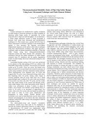
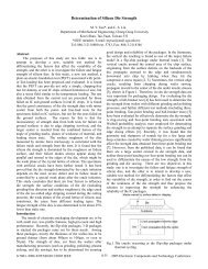
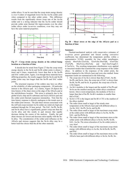
solder alloys. It can be seen that the creep strain energy densityis over 4 orders <strong>of</strong> magnitude lower for the Au-Sn solder jointwhen compared to the other solder joints. This differenceresults from the significantly slower creep rate <strong>of</strong> the Au-Snsolder and is a strong indicator that the Au-Sn solder shouldprovide solder joint thermal life improvements over the othersolder alloys under in-service conditions, even they may nothave the same material properties.Shear stress (Pa)1.E+081.E+071.E+061.E+051.E+04Pb-SnSn-InSACAu-SnSn-BiCreep strain energy density(MPa)10.80.6SAC0.4SnBi &Pb-SnSn-In0.2Au-Sn00 5 10 15 20 25 30Time (hrs)Fig 27 - Creep strain energy density at the critical bumplocation as a function <strong>of</strong> timeIt should also be noted from Figure 27 that the creep strainenergy density in the Sn-In and Sn-Bi solder joints is almost 2times and 4 times, respectively, lower than that in the Sn-Pband SAC solder joints. Again, even though these materials havediffering properties, the results suggest that the Sn-In and Sn-Bisolder joints may last longer than the Sn-Pb and SAC solderjoints.The structural response <strong>of</strong> the solders may have an effecton the reliability <strong>of</strong> other packaging components. Of particularinterest is the AlGaAs pad. As a metric, Figure 28 depicts thetime history <strong>of</strong> the shear stress at the edge <strong>of</strong> the AlGaAs pad atthe mid-thickness location. This stress is primarily due to theglobal (GaAs chip and Si substrate) and local (AlGaAs pad andthe solder joint) thermal expansion mismatches. Note that thetime history response is directly analogous to the trends seen inthe solder-joint stresses. The pad shear stresses associated withthe stiff and creep-resistant Au-Sn solder are relatively high andunabated through the 24 hour period. The SAC, Sn-Pb, Sn-Bi,and Sn-In alloys have a significantly greater creep rate than theAu-Sn alloy and this results in pad stresses that rapidlydecrease during the course <strong>of</strong> the analysis. Finally, the padshear stresses are lowest and decrease most rapidly with the Sn-In alloy. The consideration <strong>of</strong> the solder joint influence on theAlGaAs pad stresses suggests that the Sn-In alloy may be abetter lead-free choice than the all the other materials.1.E+030 6 12 18 24Time (hr)Fig 28 – Shear stress at the edge <strong>of</strong> the AlGaAs pad as afunction <strong>of</strong> timeSummary<strong>Thermal</strong>-mechanical analysis with conservative estimates <strong>of</strong>in-service power generation and forced cooling convectivecoefficients has determined the temperature pr<strong>of</strong>iles within arepresentative <strong>VCSEL</strong> assembly for four solder metallurgies,namely 48wt%Sn-52wt%In, 42wt%Sn-58wt%Bi, 63wt%Sn-37wt%Pb, 80wt%Au-20wt%Sn and Sn(3-4)wt%Ag(0.5-0.7)wt%Cu. The resulting temperature distributions were appliedto structural models that examined the creep response <strong>of</strong> the solderalloys. In addition to the responses <strong>of</strong> the solder joints, thestresses imparted to the AlGaAs laser pad were also studied. Someimportant results are summarized in the following:1. The creep rate <strong>of</strong> Au-Sn is slower than that <strong>of</strong> SAC, Sn-Bi.Sn-Pb, and Sn-In. Also, the creep rate <strong>of</strong> SAC is slower thanSn-Bi, Sn-Pb, and Sn-In. In general, the creep rate <strong>of</strong> Sn-Inis the largest.2. Au-Sn’s modulus is the largest and the moduli <strong>of</strong> Sn-Pb andSn-In are the smallest among the solder alloys consideredherein. Above room temperature, the modulus <strong>of</strong> Sn-In islarger than that <strong>of</strong> Sn-Pb. Sn-Bi’s modulus is smaller thanthat <strong>of</strong> SAC.3. Sn-In’s CTE is the largest and Sn-Bi’s CTE is the smallest <strong>of</strong>the alloys studied.4. The order (from small to large) <strong>of</strong> the steady-statetemperature at the AlGaAs laser pad with different alloys isAu-Sn, SAC, Sn-Pb, Sn-In, and Sn-Bi.5. The order (from small to large) <strong>of</strong> the maximum creep strainat the solder joints with different alloys is Au-Sn, Sn-Bi,SAC, and Sn-Pb/Sn-In.6. The order (from small to large) <strong>of</strong> the maximum stress at thesolder joints with different alloys is Sn-In, Sn-Pb, Sn-Bi,SAC, Au-Sn. The stress relaxation <strong>of</strong> Au-Sn solder joints isvery slow!7. The order (from small to large) <strong>of</strong> the maximum creep strainenergy with different alloys is Au-Sn, Sn-In/Sn-Bi, Sn-Pb,and SAC.8. The order (from small to large) <strong>of</strong> the maximum stress at theAlGaAs laser pad with different alloys is Sn-In, Sn-Bi, Sn-1016 2006 Electronic Components and Technology Conference