Thermal Stress Analysis of a Flip-Chip Parallel VCSEL - ECA Digital ...
Thermal Stress Analysis of a Flip-Chip Parallel VCSEL - ECA Digital ...
Thermal Stress Analysis of a Flip-Chip Parallel VCSEL - ECA Digital ...

You also want an ePaper? Increase the reach of your titles
YUMPU automatically turns print PDFs into web optimized ePapers that Google loves.
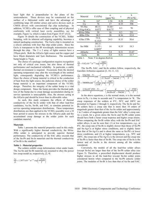
laser light that is perpendicular to the plane <strong>of</strong> thesemiconductor. These devices may be constructed on thesurface <strong>of</strong> a fabricated wafer and have the advantage <strong>of</strong>combining large 2D emitter arrays and active devices such asCMOS drivers with conventional flip chip technology. Inaddition, <strong>VCSEL</strong>s <strong>of</strong>fer ease <strong>of</strong> fiber coupling and <strong>of</strong> physicalconformity with vertical laser cavity assemblies, see forexample, Figure 1a, which is taken from Figure 10.47 <strong>of</strong> [2].Figure 1b details the construction <strong>of</strong> the <strong>VCSEL</strong>. Solderbumping, with its inherent self-aligning capability, becomes anatural packaging construction. The GaAs chip is mounted ona silicon substrate with four flip chip solder joints. Since theGaAs is transparent to the IR wavelength, transmission occursthrough the chip. The 2 x 2 array <strong>of</strong> lights sources have a250µm pitch. Both the AlGaAs light source and the copper padhave 80µm diameters and 5µm thicknesses. The assembledbump height is 75µm.The choice <strong>of</strong> a package configuration requires recognitionnot only <strong>of</strong> critical cost issues, but also those <strong>of</strong> thermalperformance and mechanical reliability. In particular, a stablethermal environment is required. Excursions from the desiredoperating temperature may alter the wavelength <strong>of</strong> the emittedlight, consequently degrading the <strong>VCSEL</strong>’s performance.Since the choice <strong>of</strong> bump material is critical to the conduction<strong>of</strong> heat from the light source, the judicious choice <strong>of</strong> the solderbump material is an important component <strong>of</strong> the <strong>VCSEL</strong>design. Therefore, the integrity <strong>of</strong> the solder bump is a vitaldesign component. Since the bump provides the thermal path,loss <strong>of</strong> the bump due to creep damage accumulation during inserviceoperation is unacceptable. Also, the stresses acting atthe AlGaAs pad should be lower than its allowable value.As such, this study compares the effects <strong>of</strong> thermalconductivity <strong>of</strong> the Sn-In solder with that <strong>of</strong> other lead-freecandidates, Au-Sn, Sn-Bi, and SAC, to simulate potential inserviceoperating temperature distributions. These temperaturedistributions are then applied to the <strong>VCSEL</strong> assembly over a 24hour period to assess the stresses in the AlGaAs pads and theaccumulated creep damage at the solder joints for eachcandidate material.MaterialsTable 1 presents the material properties used in this study.With a significantly higher thermal conductivity, the 80Au-20Sn solder is anticipated to provide superior thermalperformance. The conductivity <strong>of</strong> the SAC alloy exceeds that<strong>of</strong> the Sn-Pb and Sn-In materials and the thermal conductivity<strong>of</strong> Sn-Bi is the smallest!Table 1 - Material propertiesThe solders exhibit creep deformations when under loads.The Au-Sn and Sn-Bi materials are assumed to obey the powerlaw creep model as, respectively, [2, 9]∂ε= 1.3977x10∂t−21 σ 2.55⎛ − 9516 ⎞exp⎜⎟⎝ T ⎠Material E (GPa)αkν(ppm/°K)(W/m°K)Si 167 2.54 0.28 154Cu 76 17 0.35 39895.5Sn- 68.11- 16.66+3.9Ag-0.6Cu 0.07T 0.017T0.3 7080Au-20Sn 59 16 0.3 25148Sn-52In 30.5 28 0.36 32.863Sn-37Pb75.9-0.152T24.5 0.35 50.6Sn-58Bi381.5-3.13T+ 14 0.35 18.30.009T 2AlGaAs 86 5.8 0.31 33.67GaAs 86 5.8 0.31 33.7Table 1. Note: T in degrees Kelvin∂ε−24 ⎛ − 8483⎞= 9.82x10σ 4.05 exp⎜⎟∂t⎝ T ⎠The Sn-Pb, SAC, and Sn-In solders follow, respectively, theGar<strong>of</strong>alo-Arrhenius equation [2, 10, 11, 12]∂ε926(508 − T ) 3.3⎛σ ⎞ ⎛ − 6360 ⎞=sinh ⎜⎟exp6⎜ ⎟∂tT⎝ 37.78x10− 74414T⎠ ⎝ T ⎠∂ε5.0⎛σ ⎞ ⎛ − 5807 ⎞= 500000sinh⎜ ⎟exp8⎜ ⎟∂t⎝1x10⎠ ⎝ T ⎠11∂ε2.54x10(593 − T ) 3.11⎛σ ⎞ ⎛ − 9705 ⎞=sinh ⎜⎟exp6⎜ ⎟∂tT⎝ 36.09x10− 59628T⎠ ⎝ T ⎠In the above equations, ε is the normal strain, σ is the normalstress in Pa, t is time in seconds and T is temperature in °K. Thecreep responses <strong>of</strong> the solders at 0°C, 50°C and 100°C arepresented in Figures 2 through 4, respectively. The Sn-In and Sn-Pb solders have a creep rate that is more then 10 orders <strong>of</strong>magnitude greater than that <strong>of</strong> the Au-Sn solder and approximately1 to 2 orders <strong>of</strong> magnitude greater than the SAC alloy’s creep rate.As a result, for a given stress the Sn-In and Sn-Pb solder jointsshould have both a faster creep response and higher creep strains.When comparing the Sn-Bi solder alloy with the Sn-Pb and SACsolder alloys, it can be seen that: (1) at low temperatures, e.g., at0 o C, the creep rate <strong>of</strong> Sn-Bi is slightly slower than those <strong>of</strong> Sn-Pband Sn-Ag-Cu at higher stress conditions, and is slightly fasterthan that <strong>of</strong> Sn-Ag-Cu and is about the same as Sn-Pb’s at lowerstress conditions, and (2) at higher temperatures, e.g., 50 o C and100 o C, the creep rate <strong>of</strong> Sn-Ag-Cu is the slowest and the creep rate<strong>of</strong> Sn-Pb is faster than that <strong>of</strong> Sn-Bi. The creep rate <strong>of</strong> Sn-In is thefastest and <strong>of</strong> Au-Sn is the slowest among all the soldersconsidered.Conversely, the moduli <strong>of</strong> all the lead-free solder alloys(except Sn-In) are larger than that <strong>of</strong> the Sn-Pb solder alloy (seeFigure 5). Therefore, a prescribed displacement should producehigher stresses in all the lead-free (except Sn-In) solder jointsconsidered herein when compared to the Sn-Pb eutectic solderjoints. The modulus <strong>of</strong> Sn-Bi is less than that <strong>of</strong> Au-Sn and SAC.1010 2006 Electronic Components and Technology Conference