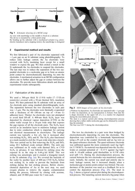
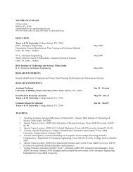
Fig. 1 Schematic drawing <strong>of</strong> a MCBJ setupAu wire <strong>with</strong> nanobridge in the middle is fixed on a substrateThe device is mounted by a three-<strong>point</strong> setupBy bending up the substrate <strong>with</strong> a mechanical actuator (e.g. piezoelectrictransducer <strong>and</strong> a stepping motor), the nanobridge is elongated2 Experimental method <strong>and</strong> resultsWe first fabricated a pair <strong>of</strong> Au electrodes separated <strong>with</strong>1 mm gap on an Si substrate using photolithography. Toreduce ionic leakage current, the Au electrodes werecovered <strong>with</strong> Si 3 N 4 insulating layer except for a smallwindow to expose the gap. We then etched a trench in theSi underneath the Au electrodes to suspend the electrodes.The last step was to reduce the separation <strong>of</strong> the two suspendedelectrodes to a <strong>molecular</strong> gap or to form an <strong>atomic</strong><strong>point</strong> contact by electrochemically depositing Au onto theelectrodes. A mechanical actuation in an MCBJ configurationallows one to further adjust the gap or contact between theelectrodes. We provide more fabrication details <strong>and</strong> discussexperimental results subsequently.2.1 Fabrication <strong>of</strong> the deviceWe used a 360-mm thick Si (1 0 0) wafer (7–13 V cmresistivity) covered <strong>with</strong> a 50 nm thermal SiO 2 insulationlayer. We then patterned the Si substrate <strong>with</strong> an array <strong>of</strong>Au electrode pairs using st<strong>and</strong>ard photolithography tools.The separation between the two electrodes in each pairwas 1 mm. The Au electrodes were thermally evaporated<strong>with</strong> a thickness <strong>of</strong> 60–100 nm on top <strong>of</strong> 8-nm Cradhesion layer. Thicker Au electrodes were not attemptedto avoid hard lift-<strong>of</strong>f. A 400-nm thick Si 3 N 4 layer wasdeposited by chemical vapour deposition (CVD) on theentire wafer except for a 10-mm wide strip that exposesthe gap regions <strong>of</strong> all the electrode pairs. The Si 3 N 4 layerserved as an insulation layer to minimise leakage currentdue to ionic conduction which is important for carryingout electrical measurement in electrolytes. The leakagecurrent was typically a few pA, but it increased afterwet-etching Si 3 N 4 , SiO 2 <strong>and</strong> Si. The Si 3 N 4 also functionedas a mask needed to etch the 10-mm wide strip into a trench.This was carried out by first removing the Si 3 N 4 <strong>and</strong> SiO 2using 20:1 buffered oxide etchant (BOE). The etch ratewas calibrated on Si wafer <strong>with</strong> thermal SiO 2 or CVDSi 3 N 4 in advance. It was followed by etching away theexposed Si in the strip in 0.44 g/ml KOH. This wetetching was anisotropic <strong>and</strong> it created a triangular trenchin the Si substrate (Fig. 2a). We covered the backside <strong>of</strong>the wafer by another layer <strong>of</strong> 400 nm CVD Si 3 N 4 beforewet etching Si, in order to prevent the backside frometching during the last etching process. Before electrochemicaldeposition <strong>of</strong> Au in the next step, we usedoxygen plasma to remove the organic contaminationduring the process, followed by rinsing <strong>with</strong> acetone,ethanol, <strong>and</strong> 18-MV pure water for 5 min each.84Fig. 2 SEM images <strong>of</strong> two pairs <strong>of</strong> Au electrodesa Without Au deposition, Au electrodes are separated <strong>with</strong> 1 mm gapb After Au deposition, an Au nanojunction is formed. Note that theL-shape electrode in the upper left <strong>of</strong> a is a marker for alignmentduring the micr<strong>of</strong>abrication processThe inset is a typical current plot during electrodeposition processshowing that a rather stable <strong>molecular</strong> gap can be obtained by controllingthe potentialThe bias was 0.01 V during the electrodepositionThe two Au electrodes in a pair were then bridged byelectrochemically depositing Au onto the electrodes. Thedeposition was controlled by a homemade bipotentiostatusing a Pt coil as the counter electrode <strong>and</strong> an Ag wire asthe quasi-reference electrode. The quasi-reference electrodewas calibrated against the more commonly used Ag/AgCl(in 3.5 M KCl). Au material was deposited onto the Au electrodesat constant potential <strong>of</strong> 20.15 V against Ag/AgCl<strong>with</strong> 8–10 mM sodium gold thiolsulfate in 0.3 M citricacid (pH 3.5). During the electrodeposition process, thecurrent between the two electrodes was monitored continuously.Initially, the current was small <strong>and</strong> entirely due toionic leakage current, but it increased sharply when a<strong>molecular</strong> gap or <strong>atomic</strong> <strong>point</strong> contact was formed. The conductance<strong>of</strong> the junction was used as a feedback for us tocontrol the deposition process (Fig. 2b). The inset inFig. 2 shows a typical current plot during the electrodepositionprocess. The tunneling current showed a big jump whenMicro & Nano Letters, Volume 1, Issue 2
the gap width was decreased to the <strong>molecular</strong> scale. Bycontrolling the electrodeposition (solid grey line), a stable<strong>molecular</strong> scale gap can be formed, as indicated by asteady tunneling current (solid black line). After completingthe fabrication, we thoroughly rinsed the chip <strong>with</strong> 18 MVpure water to remove Au deposition solution <strong>and</strong> dried it out<strong>with</strong> N 2 gas. We then mounted it on a MCBJ setup to furthercontrol the gap or <strong>point</strong> contact mechanically.2.2 CalibrationSince the mechanical control <strong>of</strong> the gap width or <strong>point</strong>contact size is achieved by bending the chip <strong>with</strong> a PZT(AE0203D08 piezoelectric stack, THORLAB Inc.), it isnecessary to calibrate the actual separation <strong>of</strong> the electrodesfor a given amount <strong>of</strong> PZT movement. Displacement ratio r,defined as the ratio <strong>of</strong> the elongation <strong>of</strong> the PZT over theinduced electrode separation, serves this calibrationpurpose. This ratio is given by r ¼ L 2 /3 mH, where L isthe distance between the two counter supports, m is thewidth <strong>of</strong> the trench <strong>and</strong> H is the thickness <strong>of</strong> the substrate(Fig. 1). In our setup, L ¼ 12 mm, m ¼ 10 mm <strong>and</strong>H ¼ 360 mm, the calculated ratio is 1.3 10 4 . To determinethe displacement ratio experimentally, we recordedthe tunneling current while applying a triangular wave tothe PZT driver. Similar displacement ratio was obtainedfrom three different devices, <strong>of</strong> which a typical one isshown in Fig. 3. From the tunneling current, we estimatedthe gap width using relation, I ¼ (2e 2 /h)V * exp(2bd),where I is the tunneling current, e is the electron charge,h is the Planck constant, V is the applied bias voltageacross the gap, d is the gap width <strong>and</strong> b, the tunnelingdecay constant in solution, is in the order <strong>of</strong> 10 nm 21[28]. According to the high <strong>and</strong> low stable tunnelingcurrent in Fig. 3, at a fixed bias voltage <strong>of</strong> 0.01 V, the correspondingelectrode separation was varied by 0.075 nm.Since the sensitivity <strong>of</strong> the PZT is 0.06 mm/V <strong>and</strong> thevoltage change in the PZT drive was 11.5 V, the elongation<strong>of</strong> PZT was determined to be 0.69 mm. Using these parameters,the measured displacement ratio was found to be1 10 4 , which is close to the theoretical estimate. Thisratio is large, so a large PZT movement is demagnifiedinto a small change in the gap width. This is the reasonfor the good stability <strong>of</strong> the setup, but it also limits thetotal adjustable range <strong>of</strong> the gap to 1 nm, <strong>with</strong> themaximum elongation <strong>of</strong> 9 mm <strong>of</strong> PZT in our setup. Theproblem associated <strong>with</strong> this limited mechanicallyFig. 3 Calibration <strong>of</strong> the displacement ratio, rThe PZT driver was modulated <strong>with</strong> a triangular wave (grey colour)<strong>and</strong> the associated tunneling current is recorded vs time (black colour)The bias in the calibration was 0.01 Vadjustable range is solved by combining it <strong>with</strong> electrochemicaletching <strong>and</strong> deposition, which provides an additionalcontrol <strong>of</strong> the size <strong>of</strong> the metal <strong>junctions</strong>. We note that sinceonly a small amount <strong>of</strong> mechanical adjustment is used in oursetup, it reduces the likelihood <strong>of</strong> breaking the Si substrate.We found that if we deposit a large amount <strong>of</strong> metal tobridge the gap, it will require a large mechanical movementto re-open the gap, which <strong>of</strong>ten causes the Si substrate tobreak. The mechanical breakdown <strong>of</strong> the Si substrate wasthe reason that the yield <strong>of</strong> the entire process was around50%, over a total <strong>of</strong> 200 devices. Once a device wasfabricated successfully, it could be used repeatedly. But inorder to minimise possible contamination, we use newdevices daily.2.3 Electron transport in 4,4 0 -bipyridineWe have used this method to study electron transport in4,4 0 -bipyridine. The molecule is terminated <strong>with</strong> two pyridinegroups which can bind to Au electrodes. It is expectedto be relatively conducting due to its conjugated structure.Finally, 4,4 0 -bipyridine is soluble in aqueous solution,which allows us to study the electrochemical gate effect.We performed the conductance measurement by breakingan Au contact in 1 mM 4,4 0 -bipyridine aqueous solution(<strong>with</strong> 0.05 M NaClO 4 as supporting electrolyte for potentialcontrol). During the breaking process, we first observedconductance quantisation associated <strong>with</strong> breakup <strong>of</strong> thegold contact (Fig. 4a). Clean quantisation steps show thatthe Au junction formed by electrodeposition was continuous<strong>and</strong> fresh. When the gold contact was completely broken,steps <strong>with</strong> smaller conductance showed up (Fig. 4b). Ourresults indicate that these steps are due to the formation <strong>of</strong>Au–4,4 0 -bipyridine–Au junction <strong>with</strong> different number <strong>of</strong>molecules trapped between the two Au electrodes. Fig. 4cis a conductance histogram constructed from 180 individualtraces such as those shown in Fig. 4b. A pronouncedconductance peak located at 0.01G 0 was revealed, whichis consistent <strong>with</strong> the previously published STM breakjunction result [29]. Broad width <strong>of</strong> conductance peakreflects the variable molecule–electrode contact geometriesin the formation <strong>of</strong> <strong>molecular</strong> <strong>junctions</strong>.To measure the I–V curves <strong>of</strong> the <strong>molecular</strong> <strong>junctions</strong>,we adjusted the electrode separation by controlling thePZT until the conductance locked on a stable plateau, correspondingto the formation <strong>of</strong> a single molecule junction, <strong>and</strong>then froze the PZT <strong>and</strong> measured the current while sweepingthe bias voltage. The bias range studied here wasbetween 20.4 V <strong>and</strong> þ0.4 V, beyond which the junctionbecame increasingly unstable. This instability is likely dueto the fact that the N–Au binding is relatively weak <strong>and</strong>4,4 0 -bipyridine desorbs from Au surfaces at negative potentials.We found that if thiol anchoring groups are used tobridge molecules to Au electrodes, the bias voltage rangecould be exp<strong>and</strong>ed to +1.2 V, due to stronger S–Aubinding. For comparison, the I–V data previously obtained<strong>with</strong> an STM setup [29] is also shown as grey solid squares,which shows that the two methods are consistent <strong>with</strong> eachother (Fig. 5a).We have studied the electrochemical gate effect on theconductance <strong>of</strong> single 4,4 0 -bipyridine <strong>with</strong> the setup. Theelectrochemical gate was controlled by a homemadebipotentiostat using a Pt wire as the counter electrode <strong>and</strong>an Ag wire as the quasi-reference electrode. The quasi referenceelectrode was calibrated against the more commonlyused Ag/AgCl (in 3.5 M KCl) reference electrode. Tomeasure the gate effect, we created a stable 4,4 0 -bipyridinejunction <strong>and</strong> then monitored the current through theMicro & Nano Letters, Volume 1, Issue 2 85