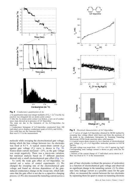
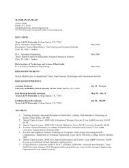
Fig. 4 Conductance quantisation <strong>of</strong> Aua Au quantisation steps near integer multiples <strong>of</strong> G 0 ¼ 2e 2 /h as the Aujunction was elongated into an <strong>atomic</strong> <strong>point</strong> contactb After the Au <strong>atomic</strong> <strong>point</strong> contact was broken, a new set <strong>of</strong> conductancesteps showed up in presence <strong>of</strong> 4,4 0 -bipyridineThe steps are due to the formation <strong>of</strong> Au–4,4 0 -bipyridine–Au<strong>junctions</strong>c Conductance histogram <strong>of</strong> 4,4 0 -bipyridine constructed from 180individual curves displays conductance peak at 0.01G 0 <strong>and</strong> 0.02G 0Grey solid lines are the Gaussian fittingBias was 0.1 V in the measurementmolecule while sweeping the electrochemical gate voltage,during which the bias voltage between two Au electrodeswas fixed at 0.1 V. A typical source-drain current (I sd )against gate voltage (V g ) curve is shown in Fig. 5b.Source-drain current increased 25%, as the gate voltagewas swept negatively. There was a run-to-run variation,but statistical analysis based on 17 different <strong>junctions</strong>showed only a small electrochemical gate effect (Fig. 5c).To verify the weak gate effect on 4,4 0 -bipyridine, wecarried out a series <strong>of</strong> control experiments: (1) Wechanged the sweeping rate <strong>of</strong> the electrochemical gatevoltage <strong>and</strong> found no obvious dependence <strong>of</strong> the gateinducedconductance change on the sweep rate, which indicatesthat the gate effect is not due to a capacitive chargingprocess. (2) We also measured the tunneling current across a86Fig. 5 Electrical characteristics <strong>of</strong> 4,4 0 -bipyridineaI–V curves <strong>of</strong> single 4,4 0 -bipyridine obtained by MCBJ method bysweeping bias voltage (black solid lines) <strong>and</strong> from the positions <strong>of</strong>the peaks in the conductance histograms by Scanning TunnelingMicroscope (STM) break <strong>junctions</strong> (grey solid squares)b A typical source-drain current (I sd ) as a function <strong>of</strong> electrochemicalgate voltage (V g ) <strong>of</strong> a 4,4 0 -bipyridine <strong>molecular</strong> junction in 0.05 MNaClO 4The gate voltage was swept from 20.2 V to þ0.6 V against Ag/AgClCorresponding ionic leakage current is shown as grey solid line forcomparisonc Statistic <strong>of</strong> the current change <strong>of</strong> 17 individual curves shown in bBias was fixed at 0.1 V in the measurementpair <strong>of</strong> bare electrodes (<strong>with</strong>out the presence <strong>of</strong> molecules)as a function <strong>of</strong> electrochemical gate voltage <strong>and</strong> observedno significant change in the tunneling current. (3) To eliminateionic leakage current as a possible cause for the gateeffect, we measured the current between the two electrodesby separating them far apart to ensure no tunneling electronsMicro & Nano Letters, Volume 1, Issue 2
can flow between the electrodes. The current was typicallywell below 0.2 nA in the electrolyte shown as the grey solidline in Fig. 5b, much smaller than the conduction currentthrough the <strong>molecular</strong> junction. The electrochemical gateeffect observed here is rather weak, which could be partiallydue to the screening <strong>of</strong> the gate field by the proximity <strong>of</strong> thetwo electrodes (serving as source <strong>and</strong> drain).3 Ni <strong>atomic</strong> <strong>point</strong> contactThe same setup can create <strong>atomic</strong> <strong>point</strong> <strong>contacts</strong> by eithermechanically controlling the elongation <strong>of</strong> the Au electrodesor by electrodeposition/etching process (Fig. 4a). Theuse <strong>of</strong> electrodeposition makes it easy to fabricate <strong>atomic</strong><strong>point</strong> <strong>contacts</strong> <strong>of</strong> different metals, <strong>and</strong> even a <strong>point</strong>contact between two different metals. To demonstrate thisapplication, we have fabricated Ni <strong>atomic</strong> <strong>point</strong> <strong>contacts</strong>using this combined approach. The first step is to electrochemicallydeposit Ni onto Au electrodes by holding thepotentials <strong>of</strong> the two electrodes at 21.1 V against Ag/AgCl <strong>with</strong> 0.1 M nickel sulphamate in 0.5 M boric acid(pH 3.5). We can also choose to deposit Ni onto only one<strong>of</strong> the two electrodes to fabricate an Au–Ni contact. Aftera <strong>point</strong> contact is formed, we can further control the size<strong>of</strong> the <strong>atomic</strong> <strong>point</strong> contact mechanically. Since Ni is aferromagnetic material <strong>with</strong> partial occupied d-orbital, ithas been argued that the strong exchange splitting <strong>of</strong> theelectron b<strong>and</strong>s may lift the spin degeneracy. The up- <strong>and</strong>down-spin electrons contribute independently to the electrictransport, which results in the conductance <strong>of</strong> <strong>atomic</strong> <strong>point</strong>contact located at integer multiples <strong>of</strong> e 2 /h. In the preliminaryexperiments, we have performed the measurement<strong>with</strong> a magnetic field (0.4 T). A typical conductancetrace is shown in Fig. 6a. Unlike the results <strong>with</strong>out a magneticfield (result not shown), steps near or at integer multiples<strong>of</strong> e 2 /h have rather frequently been observed in Ni<strong>point</strong> <strong>contacts</strong>. The conductance histogram (Fig. 6b) constructedfrom 18 individual curves from two differentdevices shows some evidence <strong>of</strong> conductance peakslocated at integer multiples <strong>of</strong> e 2 /h [30–32]. Furtherstudies are in progress to verify <strong>and</strong> underst<strong>and</strong> the preliminaryfindings.4 SummaryWe have described a combined mechanical <strong>and</strong> electrochemicaldeposition method to fabricate <strong>atomic</strong> <strong>point</strong> <strong>contacts</strong><strong>and</strong> <strong>molecular</strong> <strong>junctions</strong>. Using the method, we have created<strong>atomic</strong> <strong>point</strong> <strong>contacts</strong> <strong>and</strong> studied electron transport through4,4 0 -bipyridine. The setup is particularly suitable for studying<strong>atomic</strong> <strong>point</strong> <strong>contacts</strong> <strong>and</strong> <strong>molecular</strong> <strong>junctions</strong> inaqueous solutions, which is required for biologically relevantmolecules, <strong>molecular</strong> binding events <strong>and</strong> electrochemicalgate-control <strong>of</strong> single molecule conductance.5 AcknowledgmentsWe would like to thank Bingqian Xu <strong>and</strong> Joshua Hihath forthe help <strong>and</strong> acknowledge the financial support fromNSF-DMR-03-05242.6 ReferencesFig. 6 Conductance quantisation <strong>of</strong> Nia Conductance quantisation steps <strong>of</strong> a Ni <strong>atomic</strong> <strong>point</strong> contact. Thequantised conductance steps are located at integer multiples <strong>of</strong> e 2 /hb Conductance histogram constructed from 18 individual curves asshown in a1 Li, C.Z., Bogozi, A., Huang, W., <strong>and</strong> Tao, N.J.: ‘Fabrication <strong>of</strong> stablemetallic nanowires <strong>with</strong> quantized conductance’, Nanotechnology,1999, 10, pp. 221–2232 Morpurgo, A.F., Marcus, C.M., <strong>and</strong> Robinson, D.B.: ‘Controlledfabrication <strong>of</strong> metallic electrodes <strong>with</strong> <strong>atomic</strong> separation’, Appl.Phys. Lett., 1999, 14, p. 20823 Kervennic, Y.V., Thijssen, J.M., Vanmaekelbergh, D., Dabirian, R.,Jenneskens, L.W., van Walree, C.A., <strong>and</strong> van der Zant, H.S.J.:‘Charge transport in three-terminal <strong>molecular</strong> <strong>junctions</strong> incorporatingsulfur-end-functionalized tercyclohexylidene spacers’, Angew. Chem.Int. Ed. Engl., 2006, 45, pp. 2540–25424 Li, X.L., He, H.X., Xu, B.Q., Xiao, X., Tsui, R., Nagahara, L.A.,Amlani, I., <strong>and</strong> Tao, N.J.: ‘Electron transport properties <strong>of</strong>electrochemically <strong>and</strong> mechanically formed <strong>molecular</strong> <strong>junctions</strong>’,Surf. Sci., 2004, 573, pp. 1–105 Park, J., Pasupathy, A.N., Goldsmith, J.L., Chang, C., Yaish, Y., Petta,J.R., Rinkoski, M., Sethna, J.P., Abruna, H.D., McEuen, P.L., <strong>and</strong>Ralph, D.C.: ‘Coulomb blockade <strong>and</strong> the Kondo effect insingle-atom transistors’, Nature, 2002, 417, pp. 722–7256 Liang, W.J., Shores, M., Bockrath, M., Long, J.R., <strong>and</strong> Park, H.:‘Kondo resonance in a single-molecule transistor’, Nature, 2002,417, pp. 725–7297 Lee, J.-O., Lientschnig, G., Wiertz, F., Struijk, M., Janssen, R.A.J.,Egberink, R., Reinhoudt, D.N., Hadley, P., <strong>and</strong> Dekker, C.:‘Absence <strong>of</strong> strong gate effects in electrical measurements onphenylene-based conjugated molecules’, Nano Lett., 2003, 3,pp. 113–1178 Luber, S.M., Strobel, S., Tranitz, H.P., Wegscheider, W., Schuh, D.,<strong>and</strong> Tornow, M.: ‘Nanometre spaced electrodes on a cleavedAlGaAs surface’, Nanotechnology, 2005, 16, pp. 1182–11859 Kubatkin, S., Danilov, A., Hjort, M., Cornil, J., Bredas, J.-L.,Stuhr-Hansen, N., Hedegard, P., <strong>and</strong> Bjornholm, T.: ‘Single-electrontransistor <strong>of</strong> a single organic molecule <strong>with</strong> access to several redoxstates’, Nature, 2003, 425, pp. 698–70110 Zhitenev, N.B., Meng, H., <strong>and</strong> Bao, Z.: ‘Conductance <strong>of</strong> small<strong>molecular</strong> <strong>junctions</strong>’, Phys. Rev. Lett., 2002, 92, pp. 186805/186801–186805/18680411 Ghosh, S., Halimun, H., Mahapatro, A.K., Choi, J., Lodha, S., <strong>and</strong>Janes, D.: ‘Device structure for electronic transport throughindividual molecules using nanoelectrodes’, Appl. Phys. Lett., 2005,87, p. 233509Micro & Nano Letters, Volume 1, Issue 2 87