
You also want an ePaper? Increase the reach of your titles
YUMPU automatically turns print PDFs into web optimized ePapers that Google loves.
Introduction<br />
<strong>Drive</strong> ESCON <strong>With</strong> HOTLink<br />
The IBM® ESCON (Enterprise System CONnection) interface<br />
is presently experiencing rapid growth. Originally designed<br />
as a replacement for the older block-mux channel, it<br />
is also finding use as a high-performance system interface.<br />
This once IBM-proprietary interface is presently being processed<br />
to become an ANSI standard interface (known as SB-<br />
CON) for computer to peripheral interconnect.<br />
This application note contains an overview of ESCON operation<br />
and a design example of an ESCON physical interface,<br />
including a number of the low-level ESCON state machines<br />
(including the VHDL source code), implemented using HOT-<br />
Link and a pASIC field programmable gate array.<br />
Channels<br />
The term channel, when referring to mainframes, carries a<br />
specific meaning. Rather than representing the connection<br />
between pieces of equipment, here it also represents a significant<br />
piece of equipment as well. The channel is, in effect,<br />
a sophisticated and intelligent DMA engine whose purpose is<br />
Host<br />
CPU<br />
Bus<br />
Tag<br />
Bus<br />
Tag<br />
String<br />
Control<br />
Disk<br />
Disk<br />
Disk<br />
Storage<br />
Director<br />
Storage<br />
Director<br />
String<br />
Control<br />
Disk<br />
Disk<br />
Disk<br />
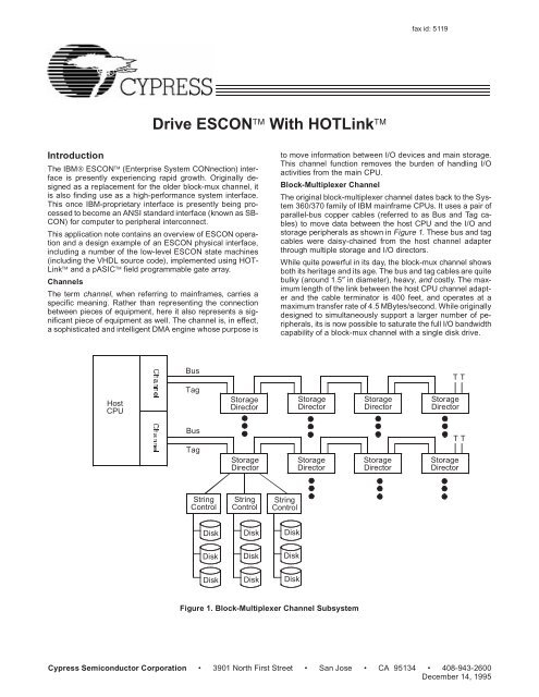
Figure 1. Block-Multiplexer Channel Subsystem<br />
fax id: 5119<br />
to move information between I/O devices and main storage.<br />
This channel function removes the burden of handling I/O<br />
activities from the main CPU.<br />
Block-Multiplexer Channel<br />
The original block-multiplexer channel dates back to the System<br />
360/370 family of IBM mainframe CPUs. It uses a pair of<br />
parallel-bus copper cables (referred to as Bus and Tag cables)<br />
to move data between the host CPU and the I/O and<br />
storage peripherals as shown in Figure 1. These bus and tag<br />
cables were daisy-chained from the host channel adapter<br />
through multiple storage and I/O directors.<br />
While quite powerful in its day, the block-mux channel shows<br />
both its heritage and its age. The bus and tag cables are quite<br />
bulky (around 1.5″ in diameter), heavy, and costly. The maximum<br />
length of the link between the host CPU channel adapter<br />
and the cable terminator is 400 feet, and operates at a<br />
maximum transfer rate of 4.5 MBytes/second. While originally<br />
designed to simultaneously support a larger number of peripherals,<br />
its is now possible to saturate the full I/O bandwidth<br />
capability of a block-mux channel with a single disk drive.<br />
String<br />
Control<br />
Storage<br />
Director<br />
Storage<br />
Director<br />
Storage<br />
Director<br />
Storage<br />
Director<br />
Storage<br />
Director<br />
Storage<br />
Director<br />
Cypress Semiconductor Corporation • 3901 North First Street • San Jose • CA 95134 • 408-943-2600<br />
December 14, 1995<br />
Disk<br />
Disk<br />
Disk<br />
TT<br />
TT
ESCON Channel<br />
The ESCON channel was introduced in 1990 along with the<br />
ESA390 series of mainframe computers. It uses high-speed<br />
serial, point-to-point fiber-optic links to replace the daisy-chained<br />
parallel-bus copper cables of a block-mux channel.<br />
By maintaining the same host CPU software structures<br />
used with the block-mux channel, it was possible to dramatically<br />
change the architecture (and performance) of the I/O<br />
subsystem without effecting the major I/O routines present in<br />
the host CPU and channel microcode.<br />
This new interconnect media was also merged with a dynamic<br />
switched connection scheme to improve both availability<br />
and access to the I/O peripherals. The use of switches<br />
(known as directors) allows many more paths to each peripheral,<br />
with multiple paths being active through each director at<br />
the same time. This new interconnect structure is shown in<br />
Figure 2. This switched I/O structure is now finding popular<br />
use in many other data communications interfaces like<br />
switched Ethernet, ATM, and Fibre Channel.<br />
The ESCON interface provides numerous improvements<br />
over the older block-mux channel. A few of these are<br />
• Improved transfer rate to 20 MBytes/second<br />
• Longer distances-up to 3 km for each link and up to three<br />
links (two switches) between Channel and Control Unit<br />
• Immunity from EMI/EMC concerns<br />
Channel<br />
Subsystem<br />
Channel<br />
Subsystem<br />
Director<br />
(Dynamic<br />
Switch)<br />
Figure 2. ESCON Channel Subsystem<br />
2<br />
<strong>Drive</strong> ESCON with HOTLink<br />
• Improved access, redundancy, and availability through use<br />
of dynamic switches<br />
ESCON Physical<br />
The physical-level interconnections of ESCON are all made<br />
with 1300-nm LED-based optical links. These links operate<br />
through either 62.5 mm or 50 mm core multi-mode optical<br />
fibers at a fixed bit rate of 200 Mbits/second. This bit rate<br />
represents the encoded bit rate for the data being sent.<br />
The data sent across ESCON links is encoded using the<br />
8B/10B code built into HOTLink. (See the CY7B923/933 data<br />
sheet for a detailed description of the 8B/10B code.) This<br />
code converts normal 8-bit bytes into 10-bit transmission<br />
characters. While this encoding does have a 25% overhead,<br />
the benefits of using it far outweigh the data-rate penalty.<br />
Part of the reason for the two extra bits in each character is<br />
to guarantee a minimum transition density for the receive<br />
PLL. Since no clock is present in the serial data, the HOTLink<br />
receiver PLL is used to extract a bit-rate clock from the data<br />
steam<br />
Another benefit from this code is its DC-balance characteristic.<br />
This means that, over time, the net difference of all 1-bits<br />
versus 0-bits sent is at or near zero. This DC-balance characteristic<br />
allows the optical receiver circuits to be much simpler<br />
and lower in cost by reducing the complexity of the AGC<br />
(automatic gain control) in the receiver preamplifier.<br />
Channel<br />
Subsystem<br />
ESCON I/O Ports ESCON I/O Ports ESCON I/O Ports<br />
Fiber-optic<br />
Links<br />
Control<br />
Unit<br />
Host CPU-A<br />
Fiber-optic<br />
Links<br />
Fiber-optic<br />
Links<br />
Control<br />
Unit<br />
Director<br />
(Dynamic<br />
Switch)<br />
Fiber-optic<br />
Links<br />
Host CPU-B<br />
Channel<br />
Subsystem<br />
ESCON I/O Ports<br />
Fiber-optic<br />
Links<br />
Control<br />
Unit
<strong>With</strong> a transmission character being ten bits in length, there<br />
are actually 1024 possible transmission characters. Of these<br />
possible codes, only a fraction of them meet all the run length<br />
and DC-balance coding rules. The remainder are illegal<br />
codes and are detected as errors at the receive end of the<br />
link. Most of the valid codes are used to represent the 256<br />
possible data bytes, with a few remaining legal transmission<br />
characters used for synchronization and in-band signaling.<br />
The term in-band means that all delimiters, protocol, clocking,<br />
etc., are handled through the same serial interface as the<br />
data; i.e., there are no other control lines or interfaces used<br />
for this information. The 8B/10B code provides twelve transmission<br />
characters for these in-band functions. Of these<br />
twelve characters (referred to as special characters), only six<br />
are defined for use by ESCON.<br />
Synchronization<br />
<strong>With</strong> any serial interface some form of synchronization is necessary<br />
at the receiver-end of a link. The function of synchronization<br />
is to line up the receiver bit and byte clocks with the<br />
serial data stream.<br />
Bit Synchronization<br />
Bit synchronization is performed (for the most part) automatically<br />
by the receiver PLL. As transitions are detected, the<br />
phase detector in the receiver uses the position of the transition<br />
(relative to its internal bit-clock) to adjust the phase and<br />
frequency of the local bit-clock. This local bit-clock is optimally<br />
adjusted to allow the serial data stream to be sampled at the<br />
center of each bit. However, bit synchronization alone is not<br />
sufficient to recover and decode the transmitted information.<br />
This requires knowledge of which bit in the serial stream is<br />
the start of a character.<br />
Framing<br />
Proper detection of character boundaries is referred to as<br />
framing. Unlike bit synchronization, which occurs primarily in<br />
the analog domain, framing is a full-digital operation.<br />
Framing is performed by examining the serial bit stream for a<br />
specific pattern (called a comma). This test occurs on every<br />
bit-clock until an exact match is found. At this point the receiver<br />
byte-clock is reset to line up with the character boundary.<br />
Following this, all characters output from the receiver should<br />
remain properly synchronized, until some external event<br />
causes a significant disruption in the data stream.<br />
The comma in the 8B/10B code is the seven bit pattern<br />
0011111 (or its alternate 1100000). This bit pattern is part of<br />
the K28.5 special character. It cannot appear in any other<br />
location in any 8B/10B encoded character, and cannot be<br />
generated across the boundaries of any pair of characters.<br />
While the detection of individual bits is controlled automatically<br />
by the PLL, the detection of framing for ESCON must be<br />
under the control of a separate state machine. This machine<br />
determines under what conditions the receiver is allowed to<br />
perform its framing function.<br />
ESCON Synchronization<br />
An ESCON interface is normally considered to be in one of<br />
two states regarding synchronization; either<br />
Synchronization_Acquired or Loss_Of_Synchronization<br />
(LOS). The transitions between these two primary states actually<br />
involve a number of substates that track error condi-<br />
3<br />
<strong>Drive</strong> ESCON with HOTLink<br />
tions and special characters on the interface. This state machine<br />
is shown in Figure 3.<br />
CT
ters are received without error, the machine reverts back to<br />
the basic Sync_Acquired state.<br />
If, however, additional character errors are detected, the state<br />
machine will advance through the SA1, SA2, and SA3<br />
states-one change for each character received in error. At<br />
each of these states the machine will again check for valid<br />
characters and will revert to the previous state if fifteen are<br />
received without any errors. This would allow an interface<br />
receiving exactly one error every sixteen characters to remain<br />
in the SA0 and SA1 states, while a similar interface receiving<br />
one error every fifteen characters would quickly move to the<br />
LOS state and remain there.<br />
Link-Level Operations<br />
The actual functionality of an ESCON link is defined in terms<br />
of various ordered sets of special characters and data bytes.<br />
These ordered sets are used to define frame boundaries,<br />
control dynamic connections, and control synchronization between<br />
the transmitter and receiver circuits. All valid ESCON<br />
ordered sets are listed in Table 1.<br />
Table 1.ESCON Ordered Sets.<br />
Ordered Set Characters<br />
Idle function K28.5<br />
Connect-start-of-frame<br />
delimiter<br />
K28.1 K28.7<br />
Passive-start-of-frame delimiter K28.5 K28.7<br />
Abort delimiter K28.6 K28.4<br />
K28.4<br />
Disconnect-end-of-frame<br />
K28.6 K28.1<br />
delimiter<br />
K28.1<br />
Passive-end-of-frame delimiter K28.6, K28.2<br />
K28.5<br />
Not-operational K28.5 D0.2<br />
Unconditional-disconnect<br />
sequence<br />
K28.5 D15.2<br />
Unconditional-disconnectresponse<br />
sequence<br />
K28.5 D16.2<br />
Off-line Sequence K28.5 D24.2<br />
Idle Function<br />
The K28.5 character in ESCON is used for multiple purposes.<br />
It is<br />
• the first character of many ordered sets<br />
• used to provide byte framing of the serial data stream<br />
• used as a fill or Idle character between frames and sequences<br />
Because the K28.5 character is contained in many of the other<br />
ordered sets, a single K28.5 cannot be conferred to be an<br />
Idle function until the following character is detected. If the<br />
following character is also an K28.5, then the previous K28.5<br />
is part of an Idle Function. If the following character is anything<br />
else, then the K28.5 character is part of a delimiter or<br />
sequence (or an error).<br />
4<br />
Delimiters<br />
<strong>Drive</strong> ESCON with HOTLink<br />
Delimiters are used to mark the start and end of frames.<br />
Frames are the real workhorse of the interface because they<br />
carry data. All frames have a start-of-frame delimiter (SOF)<br />
and an end-of-frame delimiter (EOF). (An Abort delimiter is<br />
considered to be a type of EOF.) These delimiters are only<br />
sent once per frame. Each frame must be separated by a<br />
minimum of four Idle characters.<br />
Sequences<br />
Sequences are used to indicate specific equipment conditions<br />
or states that cannot be identified through the use of<br />
frames. Unlike a delimiter, the ordered set defined for a specific<br />
sequence is sent repeatedly until the machine state<br />
changes or a specific response is received. At the receiver, a<br />
sequence is only detected as being valid if the defined ordered<br />
set is received a specific minimum number of times in<br />
succession.<br />
Frames<br />
Frames are used to carry information between the channel,<br />
switches, and the peripherals. Two generic types of frames<br />
exist; Link-Control and Device Level.<br />
All frames follow the same three-field format:<br />
• a 7-byte fixed-length link header<br />
• a variable-length information field (may have a length of<br />
zero for some Link-Control frames)<br />
• and a 5-byte fixed-length link-trailer field<br />
The structure of an ESCON frame is shown in Figure 4. The<br />
low-order bit of the Link Control field in the Link Header identifies<br />
the type of frame. When set to a one, the frame is a Link<br />
Control frame. When set to a zero, the frame is Device Level<br />
frame.<br />
Link-Control frames are use to manage, configure, and maintain<br />
the link itself, and range in length from 12 to 116 bytes.<br />
Device Level frames carry data between the channel and the<br />
peripheral and range in size from 17 to 1040 bytes.<br />
Frame Validation<br />
Before a frame can be processed, it must be validated as a<br />
properly received frame. This involves making sure that there<br />
are no special characters or idles in the middle of the frame,<br />
no decoding errors are detected in the serial stream, and that<br />
the CRC Field (Cyclic Redundancy Check) shows no errors.<br />
Cyclic Redundancy Check Field<br />
The CRC field contains a 16-bit redundancy check code,<br />
used to insure that the received frame contents are the same<br />
as those sent. This field is generated at the transmitting end<br />
of a link and sent as the first two bytes of the Link Trailer field.<br />
It is calculated on all bytes between the start-of-frame delimiter<br />
and the Link Trailer field.<br />
At the receiving end of the link the CRC is again generated<br />
using the received data stream. Now the CRC is generated<br />
on all bytes between the start-of-frame delimiter and the<br />
end-of-frame delimiter.<br />
The CRC code used with ESCON is that defined by the ITU<br />
V.41 standard (previously known as CCITT). The polynomial<br />
for this CRC is listed in Equation 1.<br />
x Eq. 1<br />
16<br />
x 12<br />
x 5<br />
+ + +<br />
1
2-bytes 2-bytes 2-bytes<br />
Start-of-Frame<br />
Delimiter<br />
Destination<br />
Address<br />
Source<br />
Address<br />
Link<br />
Header<br />
1-byte<br />
Link<br />
Control<br />
Normally with a code of this type the CRC remainder register<br />
is preset to an all 1s condition prior to the first bit of information<br />
being clocked through the polynomial. This is done to<br />
ensure that the polynomial will change state no matter what<br />
the data stream contains. At the end of the generation, the<br />
two bytes comprising the CRC remainder are sent as part of<br />
the data stream. At the receiving end the same process occurs,<br />
but the two CRC bytes are also clocked into the CRC<br />
register. If no errors exist in the serial stream then the contents<br />
of the CRC check register should be zero.<br />
To increase the level of protection, the CRC is handled slightly<br />
differently in an ESCON interface. Here the CRC remainder<br />
generated at the transmitter is inverted prior to sending it<br />
across the link. When it is received (correctly) the CRC check<br />
register is no longer cleared, but must be set to exactly 1D0F<br />
(hexadecimal). Any other value indicates a transmission or<br />
reception error.<br />
ESCON Design Example<br />
The following design was originally done to replace an existing<br />
ESCON protocol component that was no longer available.<br />
All VHDL source code listed here has been both simulated<br />
and tested in a functioning ESCON system.<br />
This design example covers<br />
• an ESCON-compatible optical media interface<br />
• ESCON-certified HOTLink serializer/deserializer components<br />
• a pASIC383 protocol chip containing<br />
— transmit and receive CRC circuits<br />
— parity check and generate circuits<br />
— Synchronization state machine<br />
— command code translation capability<br />
— input/output pipeline registers<br />
— miscellaneous flip-flops, muxes, and gates<br />
The design is partitioned into transmit and receive data paths,<br />
and is implemented in four active devices:<br />
• a pASIC383 containing both transmit and receive protocol<br />
functions<br />
• a CY7B923 HOTLink transmitter for serialization and<br />
8B/10B encode<br />
FRAME STRUCTURE<br />
Information<br />
Field<br />
Figure 4. ESCON Frame Format<br />
5<br />
<strong>Drive</strong> ESCON with HOTLink<br />
• a CY7B933 HOTLink receiver for deserialization and<br />
10B/8B decode<br />
• a Siemens V23806-A1-M16 ESCON fiber-optic<br />
transceiver<br />
The structure of how these components connect and major<br />
data paths are shown in Figure 5, with a complete schematic<br />
shown in Figure 6.<br />
Fiber-optic Transceiver<br />
The fiber-optic transceiver is an optoelectric device that both<br />
converts electrical signals to light (transmitter) and light into<br />
electrical signals (receiver). To operate with the ESCON interface<br />
the transceiver must meet a number of specific characteristics:<br />
• operate at 200 Mbaud<br />
• operate at 1300 nm wavelength<br />
• use 62.5-mm or 50-mm core optical fiber<br />
• meet the 0.7″ ferrule spacing and other dimensions of an<br />
ESCON optical connector<br />
In addition to these criteria, compliant transceivers must meet<br />
numerous power level, receive sensitivity, and electrical interface<br />
criteria to properly operate in an ESCON environment.<br />
Manufacturers of ESCON compatible fiber-optic transceivers<br />
include Siemens, AMP, IBM, and others.<br />
.<br />
Link<br />
Trailer<br />
0-to-104 bytes (Link Control)<br />
Information Field<br />
5-to-1028 bytes (Device Level)<br />
2-bytes 3-bytes<br />
CRC<br />
Field<br />
End-of-Frame<br />
Delimiter<br />
Link Header Field Information Field<br />
Link Trailer Field<br />
9<br />
9<br />
pASIC383<br />
RX<br />
Protocol<br />
TX<br />
Protocol<br />
Protocol<br />
CY7B923/933<br />
9 HOTLink<br />
RX<br />
9<br />
HOTLink<br />
TX<br />
SERDES<br />
Siemens<br />
V23806-<br />
A1/M16<br />
R<br />
X<br />
T<br />
X<br />
ESCON<br />
Fiber-optic<br />
Transceiver<br />
Figure 5. Design Example Structure
Figure 6. ESCON Physical I/O Interface Schematic<br />
6<br />
<strong>Drive</strong> ESCON with HOTLink<br />
6
SERDES<br />
The next section in an ESCON link is the serializer/deserializer<br />
block, also known as the SERDES. This section converts<br />
parallel bytes of information into an 8B/10B encoded serial<br />
data stream for transmission, and also converts a received<br />
8B/10B encoded serial data stream back into parallel data<br />
bytes.<br />
The Cypress CY7B923/933 HOTLink components are designed<br />
to perform this SERDES function. These components<br />
are specifically optimized to support the ESCON interface, as<br />
well as Fibre Channel, ATM (Asynchronous Transfer Mode),<br />
and proprietary communications links.<br />
These HOTLink parts are especially well suited to the ES-<br />
CON market because of their built-in 8B/10B encoders and<br />
decoders. This encode/decode function is required for ES-<br />
CON operation. By building the encode/decode into the SER-<br />
DES block, the complexity of this part of the interface design<br />
is removed from the design process. Its presence in the SER-<br />
DES block also means that hardware resources are not required<br />
elsewhere to implement the encode/decode function.<br />
The 8B/10B code used in the HOTLink components is licensed<br />
by Cypress Semiconductor from IBM. Any user of<br />
these parts is fully licensed to use the 8B/10B encoders and<br />
decoders contained in them at no cost and no royalties. For<br />
those applications that already have 8B/10B encoder/decoder<br />
circuits present in their system, the encoder/decoder<br />
present in HOTLink can be bypassed through use of the<br />
MODE pin on each part.<br />
An in-depth explanation of the operation and usage of the<br />
HOTLink components may be found in the CY7B923/933<br />
data sheet and the HOTLink User’s Guide.<br />
Serial I/O Electrical Interface<br />
The interface between the fiber-optic transceiver and the<br />
HOTLink SERDES operates at 200 Mbits/second. This interface<br />
is implemented with ECL (Emitter-Coupled-Logic) signaling<br />
to provide a low-noise, high-speed connection. Unlike<br />
standard ECL, which is normally operated below ground, both<br />
the fiber-optic transceiver and the HOTLink SERDES components<br />
are operated above ground. This allows the ECL portion<br />
of the design to use the same +5V supply as the surrounding<br />
logic. When ECL is operated from a positive supply<br />
it is referred to as Positive-ECL or PECL.<br />
The source for the serial data stream is the CY7B923 HOT-<br />
Link transmitter shown in Figure 6. A simplified schematic<br />
showing just the interconnect for the serial transmit path is<br />
shown in Figure 7. The serial data is connected to the fiber-optic<br />
transmitter using a differential connection from the<br />
OUTA± differential output of the HOTLink transmitter. Because<br />
these are ECL/PECL signals, they require a pull-down<br />
bias to allow the outputs to switch.<br />
<strong>With</strong> a transmission rate of 200 Mbits/second, the interconnect<br />
used for these signals should (in most cases) be constructed<br />
as a controlled-impedance transmission line. The<br />
bias network used on the OUTA± signals is referred to as a<br />
Y-bias network. It is designed to provide an equivalent transmission<br />
line termination impedance of 50Ω while providing a<br />
bias level of VCC –2V.<br />
The received serial data stream is output from the fiber-optic<br />
receiver as a differential signal, as shown in Figure 6, and is<br />
sent to the CY7B933 HOTLink receiver INA± inputs. A simpli-<br />
7<br />
<strong>Drive</strong> ESCON with HOTLink<br />
fied schematic showing just the interconnect of the serial receive<br />
path is shown in Figure 8. Because this is also a PECL<br />
signal, it should be treated in a manner similar to the transmit<br />
serial path. This means controlled impedance transmission<br />
lines and a proper bias/termination network.<br />
While the receive-path bias/termination network may be implemented<br />
using the same Y-bias network used with the<br />
transmit serial path, a Thévenin network is shown here.<br />
These two bias networks, when used with differential signals,<br />
are effectively interchangeable. For single-ended signals requiring<br />
the same electrical characteristics, the Thévenin network<br />
must be used. For additional information on terminating<br />
and biasing PECL signals, please see the application note<br />
“HOTLink Design Considerations” in the HOTLink User’s<br />
Guide.<br />
CY7B923<br />
TO RECEIVER<br />
INB+<br />
OUTA+<br />
OUTA–<br />
OUTB+<br />
OUTB–<br />
OUTC+<br />
OUTC–<br />
270Ω<br />
270Ω<br />
+5V<br />
0.1μF<br />
51Ω<br />
OPTICAL<br />
DRIVER<br />
DATA_IN<br />
/DATA_IN<br />
51Ω<br />
110Ω<br />
Figure 7. HOTLink Transmitter-to-Optical Serial Interface<br />
OPTICAL<br />
RECEIVER<br />
DATA_OUT<br />
/DATA_OUT<br />
SIG_DET<br />
/SIG_DET<br />
FROM<br />
TRANSMITTER<br />
OUTC+<br />
270Ω<br />
82Ω<br />
130Ω<br />
+5V<br />
1000pF<br />
CY7B933<br />
INA+<br />
INA–<br />
INB+<br />
INB–(SI)<br />
Figure 8. Optical-to-HOTLink Receiver Serial Interface
Serial I/O Support Interface<br />
In addition to the transmit and receive serial data streams,<br />
two other PECL signals are normally present in an ESCON<br />
interface: signal-detect and local-loopback. The signal-detect<br />
function is performed by the fiber-optic receiver. It outputs a<br />
PECL logic signal to inform the upstream hardware if a valid<br />
signal is present or not. This signal is monitored to determine<br />
the synchronization state of the interface.<br />
Because this is a PECL-level signal, it is necessary to convert<br />
it to a TTL-level signal for use by upstream logic. While there<br />
are components available that explicitly perform this level<br />
translation, they are not necessary for this application. Instead<br />
it is possible to use one of the design features of the<br />
HOTLink receiver INB± inputs to perform this signal-level<br />
conversion.<br />
The INB± input can be configured as either a differential<br />
PECL receiver (like INA±), or as a single-ended serial PECL<br />
receiver and a PECL-to-TTL converter. To use INB± as a differential<br />
receiver it is necessary to pull the SO (Status Out)<br />
pin to VCC . This disables the PECL-to-TTL converter and<br />
maintains both inputs as a differential pair.<br />
To use INB± as two separate inputs requires that the SO pin<br />
be loaded as a normal TTL-level output. When configured this<br />
way the INB– pin is the input for the PECL-to-TTL converter,<br />
with SO being the TTL output. This is the configuration used<br />
in Figures 6 and 8.<br />
Most ESCON interfaces are also equipped with numerous<br />
self-diagnostic capabilities. At the physical interface the most<br />
common is a selectable loopback of the serial data stream.<br />
This allows all components (with the exception of the fiber-optic<br />
transceiver) of the interface to be tested by transmitting<br />
data and verifying that it can be properly received. This loopback<br />
function is normally implemented using the OUTC+ output<br />
of the HOTLink transmitter and the INB+ input on the<br />
HOTLink receiver in a single-ended PECL connection, as<br />
shown in Figures 6, 7, and 8.<br />
While the best PECL connection is always a differential connection<br />
(like that used on INA±), the usage of INB+ in a single-ended<br />
mode is fine under these conditions. Because the<br />
HOTLink transmitter and receiver are close together in the<br />
system and operate from a common power supply, the normal<br />
noise-margin concerns of single-ended connections do not<br />
apply.<br />
This local loopback functionality is selected through the<br />
LOOPBACK signal on the pASIC FPGA. When active<br />
(HIGH), this signal drives the HOTLink receiver A/B select<br />
input LOW to selected the INB+ input for the deserializer, and<br />
drives the FOTO input to the HOTLink transmitter HIGH. This<br />
FOTO pin is used to disable the OUTA± and OUTB± outputs<br />
of the transmitter. This is normally done during loopback diagnostics<br />
to prevent the diagnostic data from being interpreted<br />
at the other end of the fiber-optic link.<br />
ESCON Protocol Controller<br />
The control of the serial data stream is performed using a<br />
pASIC383 FPGA. This part has been programmed to manage<br />
both the transmit and receive serial data streams. The<br />
programming and verification were done using VHDL (VHSIC<br />
Hardware Description Language) using Cypress’s Warp3<br />
logic synthesis and simulation tools. Complete source code<br />
of the design VHDL modules is listed in Appendixes A<br />
8<br />
<strong>Drive</strong> ESCON with HOTLink<br />
through H of this application note, and is available for download<br />
from the Cypress Bulletin Board system.<br />
The design shown in this application note is effectively a logic<br />
replacement for a Triquint GA9104 ESCON protocol chip.<br />
Due to the flexibility of the pASIC family of parts, it is possible<br />
to add, replace, or remove logic that is not optimal for a specific<br />
application. In this design, the 8B/10B encoders present<br />
in the normal GA9104 were not implemented in the pASIC383<br />
because they are already present in the HOTLink<br />
CY7B923/933. This allowed the entire functionality to be duplicated<br />
in a 2K-equivalent gate FPGA. The functions present<br />
in this design are<br />
• Transmit Path<br />
— input and output pipeline registers<br />
— parity checker and status bit<br />
— CRC generator and control state machine<br />
— Command/data mux<br />
— Command translator<br />
• Receive Path<br />
— input and output pipeline registers<br />
— CRC checker, control state machine, and status bit<br />
— parity generator<br />
— Command/data mux<br />
— Command translator<br />
• Byte-Sync State Machine<br />
Transmit Path<br />
A block diagram of the transmit path is shown in Figure 9.<br />
Data is captured into a 10-bit register on each rising edge of<br />
the transmit clock (CKW). The data consists of an 8-bit data<br />
byte, a single control line (CTXC0), and a parity bit. The<br />
CTXC0 line is used to identify whether the data on the inputs<br />
is a command code (HIGH) or a data byte (LOW). If the<br />
latched character is a data byte, the data is simultaneously<br />
presented to the CRC register, the parity checker, and the<br />
output multiplexers. At the next rising edge of the transmit<br />
clock, this data byte is clocked into the CRC register, checked<br />
for proper parity, and loaded into the output register along with<br />
TSC_D set LOW.<br />
The detection of a parity error is only a reported event, and<br />
occurs one cycle after the data (or command) is latched into<br />
the input register. Recovery from detected parity errors would<br />
normally require abnormal termination of the current frame<br />
using the Abort delimiter.<br />
The CRC/MUX Control block is the heart of the transmit path<br />
logic. It monitors the CTXC0 line to determine when to<br />
• preset the CRC register<br />
• accumulate a CRC<br />
• output the CRC bytes<br />
• translate/send command codes<br />
This block is implemented as a simple shift register that tracks<br />
the current and previous three states of CTXC0. These sixteen<br />
possible combinations (with don’t care states removed)<br />
and their resulting outputs are listed in Table 2. The VHDL<br />
source code for this block is listed in Appendix C.
CTXC0<br />
CTXD 8<br />
CTXP D Q<br />
S=1<br />
CKW<br />
PERR<br />
CRC/MUX<br />
CNTL<br />
8 8<br />
COMMAND<br />
TRANSLATE<br />
9<br />
<strong>Drive</strong> ESCON with HOTLink<br />
Figure 9. pASIC Transmit Path Block Diagram<br />
Table 2.Transmit Path Control.<br />
Receive Path<br />
CTXC0 Mux Select/CRC Control<br />
A block diagram of the receive path is shown in Figure 10.<br />
Data is captured from the HOTLink receiver into the input<br />
t+3 t+2 t+1 t+0<br />
register on each falling edge of the HOTLink recovered re-<br />
X<br />
X<br />
X<br />
0<br />
X<br />
0<br />
0<br />
1<br />
Data<br />
CRC High Byte<br />
ceive clock (CKR). Note that this could also be implemented<br />
using a rising edge clock, but that a falling edge clock was<br />
used for compatibility with the implementation being re-<br />
0 0 1 1 CRC Low Byte<br />
placed.<br />
X<br />
X<br />
X<br />
1<br />
1<br />
0<br />
1<br />
1<br />
Preset CRC<br />
Command<br />
All received data characters are clocked into the CRC register.<br />
Like the transmit path, this function is implemented in a<br />
byte-parallel form. The CRC register is synchronously preset<br />
1 0 1 1 Command<br />
if any command code is present in the input register. For all<br />
data codes it accumulates the CRC remainder.<br />
The CRC block implements the CRC-16 function in a The CRC register is constantly compared for the x’1D0F’ pat-<br />
byte-parallel fashion. This allows a full byte to be accumulattern. The output of this compare is clocked into the output<br />
ed in a single clock cycle. While this does require a much register. It is forced to a LOW for all clocks except the first<br />
larger number of XOR gates to implement than a serial CRC command character received following a data character. This<br />
function, it allows the design to be constructed from much CRC status remains valid for only one clock cycle. The VHDL<br />
slower logic. Here the main CRC register is clocked at 20 source code for this function is listed in Appendix E.<br />
MHz, rather than having to operate at a 200-MHz bit-clock<br />
rate. The VHDL source code for this function is listed in Appendix<br />
B.<br />
Just as in the transmit path, a command translation block is<br />
present in the design. This command translate block is not<br />
normally needed for new designs. For this specific design it<br />
The command-translate block is not normally needed for new was necessary to translate an existing set of command codes<br />
designs. For this specific design it was necessary to translate from the native HOTLink command set to a different set of<br />
an existing set of command codes to the native HOTLink command codes embedded in upstream logic. This block al-<br />
command set. This translation is quite simple with the logic lows the HOTLink command codes to be translated to any<br />
reduction performed manually for the transmit path. Here an host command set.<br />
8-bit input command is decoded into a 4-bit command field<br />
(with the upper four bits of the byte set to zero).<br />
The translation block actually implements circuitry to translate<br />
all twelve command codes in the 8B/10B character set. For<br />
The translation block actually implements circuitry to translate ESCON implementations this logic could be simplified be-<br />
all twelve command codes in the 8B/10B character set. For cause only half of these (six) are actually allowed for use in<br />
ESCON implementations this logic could be simplified be- ESCON ordered sets. The VHDL source code for this function<br />
cause only half of these (six) are actually allowed for use in is listed in Appendix D.<br />
ESCON ordered sets. The VHDL source code for this function<br />
is listed in Appendix D.<br />
Odd parity is generated on the output data byte and the<br />
CRXS0 status bit. This allows upstream logic to validate that<br />
The last section in the transmit path is the output pipeline the byte received is the same as that generated by the pASIC<br />
register. This block receives the multiplexed output of either FPGA.<br />
the input pipeline register, the high-CRC byte, the low-CRC<br />
byte, or the translated command. It serves to keep the data<br />
presented to the HOTLink transmitter synchronous with the<br />
transmit clock.<br />
The last block in the receive section is the output pipeline<br />
register. This block receives the multiplexed output of either<br />
the input pipeline register or the translated command. It<br />
serves to keep the data presented to the upstream logic synchronous<br />
with the receive clock.<br />
8<br />
8<br />
8<br />
8<br />
8<br />
8<br />
8 8 TXD<br />
TSC_D
Byte-Sync State Machine<br />
A block diagram of the byte-sync state machine is shown in<br />
Figure 11 The two primary structures in the machine are a<br />
4-bit counter and a controlling state machine. The controlling<br />
state machine is programmed to follow the state diagram<br />
shown in Figure 11. It tracks the state of the RVS signal from<br />
the receiver and a decode from the input register of all C5.0<br />
command codes (Idle characters). The four-bit counter is<br />
used to alternately count either valid characters (the absence<br />
of RVS) or valid Idle characters, based on the state of the<br />
machine.<br />
.<br />
RSC_D<br />
RXQ<br />
CKR<br />
8<br />
RESET<br />
IDLE<br />
R_RVS<br />
CKR<br />
BYTE-<br />
SYNC<br />
STATE<br />
MACHINE<br />
D Q<br />
Figure 11. Byte-Sync State MachineBlock Diagram<br />
The present form of this state machine was designed to duplicate<br />
the functionality of a previous implementation. Because<br />
of this it does not take into account the additional condition<br />
of Signal Detected that is generated by the fiber-optic<br />
receiver. Sufficient I/O and logic resources are still available<br />
in the FPGA to add this into the state machine equations.<br />
COMMAND<br />
TRANSLATE<br />
Design Summary<br />
The small size of the FPGA design is made possible by the<br />
enhanced functionality present in the HOTLink transmitter<br />
and receiver. This removes the need to design and implement<br />
Figure 10. pASIC Receive Path Block Diagram<br />
EN<br />
R<br />
A<br />
B<br />
C<br />
D<br />
4-BIT<br />
CNT<br />
BSYNC<br />
ERROR<br />
10<br />
8<br />
<strong>Drive</strong> ESCON with HOTLink<br />
Σ=0<br />
8 8<br />
CRXS1<br />
CRXS0<br />
CRXD<br />
CRXP<br />
the 8B/10B encoders and decoders, and provides full received<br />
character validation. The embedded PECL-to-TTL<br />
converter also allows a small footprint by removing the need<br />
for an external conversion circuit.<br />
The VHDL design both auto-routes and auto-places into a<br />
pASIC383 FPGA. Because of the high-speed operation of the<br />
pASIC cells and interconnect, this design meets or exceeds<br />
all design performance parameters, over worst case temperature<br />
and voltage, using the slow –0 speed bin of the<br />
pASIC383.<br />
The 100% routability of the pASIC family allows the circuit<br />
board signal routing to be improved by selecting pins that best<br />
match the system interconnect. The pinouts listed in the<br />
top-level VHDL file were selected to allow straight-through<br />
routing (no crossovers) of the signals between the FPGA and<br />
the HOTLink transmitter and receiver. In addition, the placement<br />
of the HOTLink transmitter and receiver were selected<br />
to line up with the transmit and receive halves of the fiber-optic<br />
transceiver. This pinout selection and interconnect are<br />
shown in Figure 12.<br />
Conclusions<br />
The ESCON interface is both an elegant and powerful replacement<br />
for the older block-mux channels. The use of the<br />
HOTLink serializer/deserializer components to implement an<br />
ESCON interface guarantees both compliance with the<br />
8B/10B coding rules and all jitter and timing specifications of<br />
the ESCON interface.<br />
Due to the high-speed operation of the ESCON interface, the<br />
byte-level control is best implemented in hardware. The flexibility<br />
of the VHDL language and the unlimited routing of the<br />
Cypress pASIC family of FPGAs make them a perfect choice<br />
for building the control state machines. While only the lower<br />
level of the ESCON protocol is controlled in the design documented<br />
here, much of the higher level control may also be<br />
implemented through the use of either larger or additional<br />
FPGA components.
CTXD5<br />
CTXD4<br />
CTXD3<br />
CTXD2<br />
CTXD1<br />
CTXD0<br />
TXCLK<br />
VCC<br />
CTXC0<br />
CY7B923<br />
TX<br />
CY7C383A-0<br />
CY7B933<br />
RX<br />
CRXD2<br />
CRXD3<br />
CRXD4<br />
CRXD5<br />
CRXD6<br />
CRXD7<br />
RXCLK<br />
RXCLK<br />
VCC<br />
RESETN<br />
CRXP<br />
LOOPEN<br />
Figure 12. HOTLink/pASIC Pinout and Interconnect<br />
Warp3 and HOTLink are trademarks of Cypress Semiconductor<br />
pASIC is a trademark of QuickLogic<br />
ESCON is a trademark of International Business Machines, Inc.<br />
IBM is a registered trademark of International Business Machines, Inc.<br />
11<br />
References<br />
<strong>Drive</strong> ESCON with HOTLink<br />
1. ESCON I/O Interface, IBM, 1990, 1991<br />
2. HOTLink User’s Guide, Cypress Semiconductor, 1995<br />
3. GA9104 Datasheet, Triquint Semiconductor, Inc, 1992
Appendix A. Top-Level pASIC Code<br />
-- ESC_TOP.VHD<br />
--<br />
-- ESCON Interface Control PLD<br />
-- Equivalent to the Triquint GA9104 but designed for operation<br />
-- with the Cypress Semiconductor HOTLink chipset<br />
ENTITY esc_top IS PORT (<br />
txclk: IN BIT; -- transmit path byte clock<br />
rxclkA: IN BIT; -- receiver path byte clock<br />
rxclkB: IN BIT; -- receiver path byte clock<br />
resetn: IN BIT; -- active low reset<br />
rxq: INOUT X01Z_VECTOR(0 TO 7); -- HOTLink receiver data in<br />
rsc_d: INOUT X01Z; -- HOTLink receiver SC/D<br />
r_rvs: INOUT X01Z; -- HOTLink receiver RVS<br />
txd: INOUT X01Z_VECTOR(0 TO 7); -- HOTLink transmitter data out<br />
tsc_d: INOUT X01Z; -- HOTLink transmitter SC/D<br />
crxd: INOUT X01Z_VECTOR(0 TO 7); -- receive path data output<br />
ctxd: INOUT X01Z_VECTOR(0 TO 7); -- transmit path data input<br />
crxs0: INOUT X01Z; -- receive status 0 (command/data)<br />
crxs1: INOUT X01Z; -- receive status 1 (CRC)<br />
ctxc0: INOUT X01Z; -- transmit control 0 (command/data)<br />
bsync: INOUT X01Z; -- byte sync acquired<br />
error: INOUT X01Z; -- receive bad character error<br />
perr: INOUT X01Z; -- transmit-in parity error<br />
crxp: INOUT X01Z; -- odd parity output<br />
ctxp: INOUT X01Z; -- odd parity input<br />
loopen: INOUT X01Z; -- local loopback enable<br />
ab_sel: INOUT X01Z); -- receiver A/B select<br />
ATTRIBUTE part_name OF esc_top:ENTITY IS “C383A”;<br />
ATTRIBUTE pin_numbers OF esc_top:ENTITY IS<br />
“txclk:17 rxclkA:53 rxclkB:54 resetn:50 rxq(7):44 rxq(6):43 ”<br />
& “rxq(5):42 rxq(4):41 rxq(3):40 rxq(2):39 rxq(1):38 rxq(0):37 ”<br />
& “rsc_d:36 r_rvs:45 txd(7):34 txd(6):33 txd(5):32 txd(4):31 ”<br />
& “txd(3):30 txd(2):29 txd(1):28 txd(0):27 tsc_d:26 crxd(0):62 ”<br />
& “crxd(1):61 crxd(2):60 crxd(3):59 crxd(4):58 crxd(5):57 ”<br />
& “crxd(6):56 crxd(7):55 ctxd(0):15 ctxd(1):14 ctxd(2):13 ”<br />
& “ctxd(3):12 ctxd(4):11 ctxd(5):10 ctxd(6):9 ctxd(7):8 ”<br />
& “crxs0:63 crxs1:64 ctxc0:21 bsync:65 error:66 perr:7 ”<br />
& “crxp:49 ctxp:6 loopen:47 ab_sel:46";<br />
END esc_top;<br />
USE work.cypress.all;<br />
USE work.rtlpkg.all;<br />
USE work.memorypkg.all;<br />
USE work.ttlpkg.all;<br />
USE work.registerpkg.all;<br />
USE work.iopkg.all;<br />
USE work.mcpartspkg.all;<br />
USE work.gatespkg.all;<br />
USE work.resolutionpkg.all; -- used to double-buffer<br />
USE work.bv_math.all; -- allow use of INV function<br />
USE work.crc_t.all; -- add in CRC transmit function<br />
USE work.crc_r.all; -- add in CRC receive function<br />
USE work.crc_ctl.all; -- add in transmit CRC control machine<br />
USE work.sync_det.all; -- add in SYNC detect state machine<br />
USE work.triq_code.all; -- add in command decoder section<br />
USE work.iopluspkg.all; -- add in enhanced I/O buffers<br />
12<br />
<strong>Drive</strong> ESCON with HOTLink
Appendix A. Top-Level pASIC Code (continued)<br />
ARCHITECTURE escon_top OF esc_top IS<br />
-- add internal signal equivalents of signals after I/O pads<br />
SIGNAL tclk : BIT; -- transmit clock<br />
SIGNAL rclk : BIT; -- negative edge receiver clock<br />
SIGNAL reset : BIT; -- reset controller<br />
SIGNAL HL_rx : BIT_VECTOR(0 to 7); -- HOTLink receiver data bus<br />
SIGNAL HL_rsc_d : BIT; -- HOTLink receiver SC/D<br />
SIGNAL HL_r_rvs : BIT; -- HOTlink receiver RVS<br />
SIGNAL HL_tx : BIT_VECTOR(0 to 7); -- HOTLink transmitter data bus<br />
SIGNAL HL_tsc_d : BIT; -- HOTLink transmitter SC/D<br />
SIGNAL HL_tsc_q : BIT; -- clocked HOTLink transmitter SC/D<br />
SIGNAL sync_r : BIT; -- receiver byte sync<br />
SIGNAL c_rxd : BIT_VECTOR(0 to 7); -- controller receive path data out<br />
SIGNAL c_txd : BIT_VECTOR(0 to 7); -- controller transmit path dataout<br />
SIGNAL c_rxs0 : BIT; -- receive status 0 (command/data)<br />
SIGNAL c_rxs1 : BIT; -- receive status 1 (CRC)<br />
SIGNAL c_txc0 : BIT; -- transmit control 0 (command/data)<br />
SIGNAL b_sync : BIT; -- byte sync acquired<br />
SIGNAL r_error : BIT; -- receive bad character error<br />
SIGNAL p_err : BIT; -- parity error<br />
SIGNAL c_rxp : BIT; -- odd parity output<br />
SIGNAL c_txp : BIT; -- odd parity input<br />
SIGNAL b_loopen : BIT; -- buffered loop enable<br />
-- transmit internal signals<br />
SIGNAL t_data : BIT_VECTOR(0 TO 7); -- transmit data bus<br />
SIGNAL t_mux : BIT_VECTOR(0 TO 7); -- muxed transmit data path<br />
SIGNAL t_comm : BIT_VECTOR(0 TO 7); -- re-encoded transmit commands<br />
SIGNAL tp_odd : BIT; -- transmit data parity input<br />
SIGNAL t_parity : BIT; -- transmit parity checker output<br />
SIGNAL t_CRC : BIT_VECTOR(0 TO 7); -- transmit CRC vector<br />
SIGNAL c_txc_0 : BIT; -- transmit command/data<br />
SIGNAL mux_hi : BIT; -- enable HI/LOW transmit CRC byte<br />
SIGNAL mux_low : BIT; -- enable LOW transmit CRC byte<br />
sIGNAL ctxc3 : BIT; -- 3x registered c_txc_0<br />
SIGNAL t_CRC_reset : BIT; -- preset transmit CRC register<br />
-- receive internal signals<br />
SIGNAL r_data : BIT_VECTOR(0 TO 7); -- registered receiver data bus<br />
SIGNAL r_mux : BIT_VECTOR(0 TO 7); -- muxed data and translated commands<br />
SIGNAL rp_odd : BIT; -- receive data parity output<br />
SIGNAL rcom_data : BIT; -- registered SC/D pin<br />
SIGNAL r_com_data: multi_buffer BIT; -- double buffered registerd SC/D pin<br />
SIGNAL r_crc_err : BIT; -- un-registered CRC status<br />
SIGNAL r_CRC_d : BIT; -- CRC check D-input<br />
SIGNAL rvs : BIT; -- registered RVS signal<br />
SIGNAL sync : BIT; -- decoded K28.5 signal<br />
SIGNAL t_code : BIT_VECTOR(0 to 7); -- Triquint pattern for K-codes<br />
---------------------------------------------------------------------------<br />
---------------------------------------------------------------------------<br />
13<br />
<strong>Drive</strong> ESCON with HOTLink
Appendix A. Top-Level pASIC Code (continued)<br />
BEGIN<br />
-- instantiate pASIC buffers/drivers on I/O signals<br />
-- clocks<br />
p1: CKPAD PORT MAP (txclk, tclk); -- transmit path clock<br />
p2: HDI2PAD PORT MAP (rxclkA, rxclkB, rclk); -- receive path clock on<br />
-- on negative edge<br />
-- high drive pads<br />
p3: HDIPAD PORT MAP (resetn ,reset); -- active HIGH system reset<br />
-- data buses<br />
-- HOTLink receiver data bus (input)<br />
p4: INPAD PORT MAP (rxq(0), HL_rx(0));<br />
p5: INPAD PORT MAP (rxq(1), HL_rx(1));<br />
p6: INPAD PORT MAP (rxq(2), HL_rx(2));<br />
p7: INPAD PORT MAP (rxq(3), HL_rx(3));<br />
p8: INPAD PORT MAP (rxq(4), HL_rx(4));<br />
p9: INPAD PORT MAP (rxq(5), HL_rx(5));<br />
p10: INPAD PORT MAP (rxq(6), HL_rx(6));<br />
p11: INPAD PORT MAP (rxq(7), HL_rx(7));<br />
p12: INPAD PORT MAP (rsc_d, HL_rsc_d); -- receive SC/D<br />
p13: INPAD PORT MAP (r_rvs, HL_r_rvs); -- RVS<br />
-- HOTLink transmitter data bus (output)<br />
p14: OUTPAD PORT MAP (HL_tx(0), txd(0));<br />
p15: OUTPAD PORT MAP (HL_tx(1), txd(1));<br />
p16: OUTPAD PORT MAP (HL_tx(2), txd(2));<br />
p17: OUTPAD PORT MAP (HL_tx(3), txd(3));<br />
p18: OUTPAD PORT MAP (HL_tx(4), txd(4));<br />
p19: OUTPAD PORT MAP (HL_tx(5), txd(5));<br />
p20: OUTPAD PORT MAP (HL_tx(6), txd(6));<br />
p21: OUTPAD PORT MAP (HL_tx(7), txd(7));<br />
p22: OUTPAD PORT MAP (HL_tsc_q, tsc_d);<br />
-- controller transmit data bus (input)<br />
p24: INPAD PORT MAP (ctxd(0), c_txd(0));<br />
p25: INPAD PORT MAP (ctxd(1), c_txd(1));<br />
p26: INPAD PORT MAP (ctxd(2), c_txd(2));<br />
p27: INPAD PORT MAP (ctxd(3), c_txd(3));<br />
p28: INPAD PORT MAP (ctxd(4), c_txd(4));<br />
p29: INPAD PORT MAP (ctxd(5), c_txd(5));<br />
p30: INPAD PORT MAP (ctxd(6), c_txd(6));<br />
p31: INPAD PORT MAP (ctxd(7), c_txd(7));<br />
-- controller receiver data bus (output)<br />
p34: OUTPAD PORT MAP (c_rxd(0), crxd(0));<br />
p35: OUTPAD PORT MAP (c_rxd(1), crxd(1));<br />
p36: OUTPAD PORT MAP (c_rxd(2), crxd(2));<br />
p37: OUTPAD PORT MAP (c_rxd(3), crxd(3));<br />
p38: OUTPAD PORT MAP (c_rxd(4), crxd(4));<br />
p39: OUTPAD PORT MAP (c_rxd(5), crxd(5));<br />
p40: OUTPAD PORT MAP (c_rxd(6), crxd(6));<br />
p41: OUTPAD PORT MAP (c_rxd(7), crxd(7));<br />
-- misc input pads<br />
p44: INPAD PORT MAP (loopen, b_loopen); -- loopback enable<br />
p45: INPAD PORT MAP (ctxc0, c_txc0); -- transmit control 0<br />
p49: INPAD PORT MAP (ctxp, c_txp); -- odd parity input<br />
-- misc output pads<br />
p50: OUTPAD PORT MAP (c_rxs0, crxs0); -- receiver status 0 output<br />
p51: OUTPAD PORT MAP (c_rxs1, crxs1); -- receiver status 1 output<br />
p53: OUTPAD PORT MAP (b_sync, bsync); -- byte sync acquired<br />
p54: OUTPAD PORT MAP (r_error, error); -- received bad character<br />
p55: OUTPAD PORT MAP (p_err, perr); -- parity error<br />
p56: OUTPAD PORT MAP (c_rxp, crxp); -- odd parity output<br />
p57: OUTPAD PORT MAP (INV(b_loopen),ab_sel); -- HOTLink receiver A/B select<br />
14<br />
<strong>Drive</strong> ESCON with HOTLink
Appendix A. Top-Level pASIC Code (continued)<br />
---------------------------------------------------------------------------<br />
-------------- TRANSMIT PATH ----------------------------------------------<br />
---------------------------------------------------------------------------<br />
-- add in transmit path input data pipeline register<br />
t1a: DFF PORT MAP (c_txd(0), tclk, t_data(0));<br />
t1b: DFF PORT MAP (c_txd(1), tclk, t_data(1));<br />
t1c: DFF PORT MAP (c_txd(2), tclk, t_data(2));<br />
t1d: DFF PORT MAP (c_txd(3), tclk, t_data(3));<br />
t1e: DFF PORT MAP (c_txd(4), tclk, t_data(4));<br />
t1f: DFF PORT MAP (c_txd(5), tclk, t_data(5));<br />
t1g: DFF PORT MAP (c_txd(6), tclk, t_data(6));<br />
t1h: DFF PORT MAP (c_txd(7), tclk, t_data(7));<br />
- add parity and control bits<br />
t1j: DFF PORT MAP (c_txp, tclk, tp_odd);<br />
t1k: DFF PORT MAP (c_txc0, tclk, c_txc_0);<br />
---------------------------------------------------------------------------<br />
-- add transmit data parity checker (10 bit parity tree)<br />
t_parity
Appendix A. Top-Level pASIC Code (continued)<br />
------------------------------------------------------------------------<br />
-- transmit path data/command/CRC mux<br />
t8: PROCESS (c_txc_0, mux_low, mux_hi)<br />
BEGIN<br />
IF (c_txc_0 = ’0’) THEN<br />
t_mux
---------------------------------------------------------------------------<br />
-- add CRC check register<br />
r5: DFF PORT MAP (r_CRC_d, rclk, c_rxs1);<br />
r_CRC_d
Appendix B. Transmit Path CRC Generator<br />
-- CRC_T.VHD<br />
--<br />
-- transmit 16-bit CCITT CRC for use in data mover<br />
--<br />
-- When sequencing bytes out, the qt(15)-qt(8) byte must be sent out first.<br />
-- Per the ESCON spec, the CRC is the 1’s compliment (inversion) of the<br />
-- qt[15:0] bus.<br />
--<br />
PACKAGE crc_T IS<br />
COMPONENT crc_tx PORT (<br />
clk, -- system clock<br />
preset: IN BIT; -- synchronous preset, set to all 1s<br />
enable: IN BIT; -- enable when not a command byte<br />
mux_hi: IN BIT; -- enable high-byte onto bus<br />
dt: IN BIT_VECTOR (0 TO 7); -- Input data byte<br />
q_out: OUT BIT_VECTOR (0 TO 7) -- CRC register<br />
);<br />
END COMPONENT;<br />
END crc_T;<br />
use work.rtlpkg.all;<br />
use work.cypress.all;<br />
ENTITY crc_tx IS PORT (<br />
clk, -- system clock<br />
preset: IN BIT; -- synchronous reset, set to all 1s<br />
enable: IN BIT; -- enable when not a command byte<br />
mux_hi: IN BIT; -- enable high CRC byte out<br />
dt: IN BIT_VECTOR (0 TO 7); -- Input data byte<br />
q_out: OUT BIT_VECTOR (0 TO 7) -- CRC register<br />
);<br />
END crc_tx;<br />
ARCHITECTURE ccitt_tx OF crc_tx IS<br />
SIGNAL qt: BIT_VECTOR (0 TO 15); -- CRC register<br />
BEGIN<br />
proc1: PROCESS BEGIN<br />
WAIT UNTIL (clk=’1’);<br />
IF (preset=’1’) THEN<br />
qt
-- mux and Invert CRC and swap bits<br />
m1: PROCESS (mux_hi)<br />
BEGIN<br />
-- Mux out high and low bytes and transpose bit order<br />
IF mux_hi = ’0’ THEN<br />
q_out(7)
Appendix C. Transmit Path CRC Controller<br />
-- CTL_CRCT.VHD<br />
--<br />
-- Control transmit CRC function<br />
--<br />
--<br />
-- All actions are based on the CTXC0 input. This input is active<br />
-- at the end of every data sequence and is a 1 (HIGH) for all<br />
-- non-data bytes.<br />
--<br />
PACKAGE crc_ctl IS<br />
COMPONENT tx_ctl_crc PORT (<br />
clk, -- transmit clock<br />
ctxc0: IN BIT; -- command/data control bit<br />
ctxc1, -- registered ctxc0<br />
ctxc2, -- 2x registered ctxc0<br />
ctxc3: OUT BIT); -- 3x registered ctxc0<br />
END COMPONENT;<br />
END crc_ctl;<br />
ENTITY tx_ctl_crc IS PORT (<br />
clk, -- transmit clock<br />
ctxc0: IN BIT; -- command/data control bit<br />
ctxc1, -- registered ctxc0<br />
ctxc2, -- 2x registered ctxc0<br />
ctxc3: OUT BIT); -- 3x registered ctxc0<br />
END tx_ctl_crc;<br />
USE work.cypress.all;<br />
USE work.rtlpkg.all;<br />
ARCHITECTURE ctl_1 OF tx_ctl_crc IS<br />
SIGNAL cq1: BIT; -- single registered c/d<br />
SIGNAL cq2: BIT; -- double registered c/d<br />
BEGIN<br />
-- Instantiate DFF to track status of ctxc0 bit<br />
d1: DFF PORT MAP (ctxc0, clk, cq1);<br />
d2: DFF PORT MAP (cq1, clk, cq2);<br />
d3: DFF PORT MAP (cq2, clk, ctxc3);<br />
-- assign outputs<br />
ctxc1
Appendix D. Command Mapper<br />
-- TRI_CODE.VHD<br />
--<br />
-- Command decode/translate between the Triquint GA9104 and HOTLink<br />
-- K-code command sets<br />
--------------------------------------------------------------------------<br />
-- Triquint/Cypress Command mapping<br />
-- GA9104 HOTLink HEX<br />
-- HEX BIN TX RX BIN<br />
-- k28.0* 1C 00011100 00 00000000<br />
-- k28.1 3C 00111100 01 00000001<br />
-- k28.2 5C 01011100 02 00000010<br />
-- k28.3* 7C 01111100 03 00000011<br />
-- k28.4 9C 10011100 04 00000100<br />
-- k28.5 BC 10111100 05,E1,E2 00000101<br />
-- k28.6 DC 11011100 06 00000110<br />
-- k28.7 FC 11111100 07,27,47 00000111<br />
-- k23.7* F7 11110111 08 00001000<br />
-- k27.7* FB 11111011 09 00001001<br />
-- k29.7* FD 11111101 0A 00001010<br />
-- k30.7* FE 11111110 0B 00001011<br />
-- * - Illegal for use in ESCON operations<br />
PACKAGE triq_code IS<br />
COMPONENT t_encode PORT (<br />
c_code : IN BIT_VECTOR(0 TO 7); -- Cypress HOTLink C-codes<br />
t_code : OUT BIT_VECTOR(0 TO 7) -- Triquint K-codes<br />
);<br />
END COMPONENT;<br />
COMPONENT t_decode PORT (<br />
t_data : IN BIT_VECTOR(0 TO 7); -- Triquint K-codes<br />
t_comm : OUT BIT_VECTOR(0 TO 7) -- Cypress HOTLink C-codes<br />
);<br />
END COMPONENT;<br />
END triq_code;<br />
USE work.cypress.all;<br />
USE work.table_bv.all; -- use for command encoder<br />
ENTITY t_encode IS PORT (<br />
c_code : IN BIT_VECTOR(0 TO 7); -- Cypress HOTLink C-codes<br />
t_code : OUT BIT_VECTOR(0 TO 7) -- Triquint K-codes<br />
);<br />
END t_encode;<br />
21<br />
<strong>Drive</strong> ESCON with HOTLink
ARCHITECTURE t_encoder OF t_encode IS<br />
-- use TTF function to translate from one command set to the other<br />
-- Command constants<br />
-- T-codes (output vectors)<br />
CONSTANT K28_0: x01_VECTOR(0 TO 7) := “00111000";<br />
CONSTANT K28_1: x01_VECTOR(0 TO 7) := “00111100";<br />
CONSTANT K28_2: x01_VECTOR(0 TO 7) := “00111010";<br />
CONSTANT K28_3: x01_VECTOR(0 TO 7) := “00111110";<br />
CONSTANT K28_4: x01_VECTOR(0 TO 7) := “00111001";<br />
CONSTANT K28_5: x01_VECTOR(0 TO 7) := “00111101";<br />
CONSTANT K28_6: x01_VECTOR(0 TO 7) := “00111011";<br />
CONSTANT K28_7: x01_VECTOR(0 TO 7) := “00111111";<br />
CONSTANT K23_7: x01_VECTOR(0 TO 7) := “11101111";<br />
CONSTANT K27_7: x01_VECTOR(0 TO 7) := “11011111";<br />
CONSTANT K29_7: x01_VECTOR(0 TO 7) := “10111111";<br />
CONSTANT K30_7: x01_VECTOR(0 TO 7) := “01111111";<br />
-- C-codes (input vectors)<br />
CONSTANT C00_0: x01_VECTOR(0 TO 7) := “0000xxxx”;<br />
CONSTANT C01_0: x01_VECTOR(0 TO 7) := “1000xxx0";<br />
CONSTANT C02_0: x01_VECTOR(0 TO 7) := “0100xxx0";<br />
CONSTANT C03_0: x01_VECTOR(0 TO 7) := “1100xxxx”;<br />
CONSTANT C04_0: x01_VECTOR(0 TO 7) := “0010xxxx”;<br />
CONSTANT C05_0: x01_VECTOR(0 TO 7) := “1010xxxx”;<br />
CONSTANT C06_0: x01_VECTOR(0 TO 7) := “0110xxxx”;<br />
CONSTANT C07_0: x01_VECTOR(0 TO 7) := “1110xxxx”;<br />
CONSTANT C08_0: x01_VECTOR(0 TO 7) := “0001xxxx”;<br />
CONSTANT C09_0: x01_VECTOR(0 TO 7) := “1001xxxx”;<br />
CONSTANT C10_0: x01_VECTOR(0 TO 7) := “0101xxxx”;<br />
CONSTANT C11_0: x01_VECTOR(0 TO 7) := “1101xxxx”;<br />
CONSTANT C12_0: x01_VECTOR(0 TO 7) := “0011xxxx”;<br />
-- errors and special mappings<br />
CONSTANT C01_7: x01_VECTOR(0 TO 7) := “1000xxx1";<br />
CONSTANT C02_7: x01_VECTOR(0 TO 7) := “0100xxx1";<br />
CONSTANT table: x01_TABLE(0 TO 13, 0 TO 15) := ( -- command mappings<br />
-- Command<br />
-- Input Output<br />
-- ----- ------<br />
C00_0 & K28_0,<br />
C01_0 & K28_1,<br />
C02_0 & K28_2,<br />
C03_0 & K28_3,<br />
C04_0 & K28_4,<br />
C05_0 & K28_5,<br />
C06_0 & K28_6,<br />
C07_0 & K28_7,<br />
C08_0 & K23_7,<br />
C09_0 & K27_7,<br />
C10_0 & K29_7,<br />
C11_0 & K30_7,<br />
C01_7 & K28_5,<br />
C02_7 & K28_5);<br />
BEGIN<br />
p1: PROCESS (c_code)<br />
BEGIN<br />
t_code
USE work.cypress.all;<br />
ENTITY t_decode IS PORT (<br />
t_data : IN BIT_VECTOR(0 TO 7); -- Triquint K-codes<br />
t_comm : OUT BIT_VECTOR(0 TO 7) -- Cypress HOTLink C-codes<br />
......................................... );<br />
END t_decode;<br />
ARCHITECTURE t_decoder OF t_decode IS<br />
BEGIN<br />
t_comm(7)
Appendix E. Receive Path CRC Checker<br />
-- CRC_R.VHD<br />
--<br />
-- receiver 16-bit CCITT CRC for use in data mover<br />
PACKAGE crc_r IS<br />
COMPONENT crc_rx PORT (<br />
clk, -- system clock<br />
preset: IN BIT; -- synchronous reset, set to all 1s<br />
dr: IN BIT_VECTOR (0 TO 7); -- Input data byte<br />
crc_err: OUT BIT -- error detected<br />
);<br />
END COMPONENT;<br />
END crc_r;<br />
use work.rtlpkg.all;<br />
use work.cypress.all;<br />
ENTITY crc_rx IS PORT (<br />
clk, -- system clock<br />
preset: IN BIT; -- synchronous preset, set to all 1s<br />
dr: IN BIT_VECTOR (0 TO 7); -- Input data byte<br />
crc_err: OUT BIT -- error detected<br />
);<br />
END crc_rx;<br />
ARCHITECTURE ccitt_rx OF crc_rx IS<br />
-- declare CRC register<br />
SIGNAL qr: BIT_VECTOR (0 TO 15); -- CRC register<br />
ATTRIBUTE POLARITY OF qr:SIGNAL IS PL_KEEP; -- maintain polarity f<br />
BEGIN<br />
proc1: PROCESS BEGIN<br />
WAIT UNTIL (clk=’1’);<br />
IF (preset=’1’) THEN<br />
qr
Appendix F. Byte Sync Controller<br />
-- B_SYNC.VHD - byte synchronization state machine<br />
--<br />
-- This machine has a five state supervisor machine that tracks<br />
-- the number of errors detected within a specific period of time.<br />
-- It also tracks valid characters and SYNC codes.<br />
PACKAGE sync_det IS<br />
COMPONENT byte_syn PORT (<br />
clk, -- Receiver clock<br />
reset, -- system reset<br />
error, -- bad character<br />
sync: IN BIT; -- valid k28.5<br />
bsync: OUT BIT); -- byte-sync acquired<br />
END COMPONENT;<br />
END sync_det;<br />
USE work.cypress.all;<br />
USE work.rtlpkg.all;<br />
USE work.counterpkg.all;<br />
ENTITY byte_syn IS PORT (<br />
clk, -- Receiver clock<br />
reset, -- system reset<br />
error, -- bad character<br />
sync: IN BIT; -- valid k28.5<br />
bsync: OUT BIT); -- byte-sync acquired<br />
END byte_syn;<br />
ARCHITECTURE arch1 OF byte_syn IS<br />
-- declare internal signals<br />
SIGNAL ctr_en: BIT; -- counter enable<br />
SIGNAL ctr_reset: BIT; -- counter reset<br />
SIGNAL bbsync: BIT; -- interface in sync<br />
SIGNAL cnt: BIT_VECTOR(0 TO 3); -- 4-bit counter vector<br />
-- declare state machine<br />
TYPE sync_state IS (<br />
state0, -- reset or errors, waiting for SYNC codes<br />
state1, -- no errors, in sync<br />
state2, -- 1 error, in sync<br />
state3, -- 2 errors, in sync<br />
state4); -- 3 errors, in sync<br />
-- declare state machine encoding, state variable, and initial state<br />
SIGNAL s_state : sync_state := state0;<br />
25<br />
<strong>Drive</strong> ESCON with HOTLink
Appendix F. Byte Sync Controller (continued)<br />
BEGIN<br />
proc1: PROCESS BEGIN<br />
WAIT UNTIL (clk=’1’);<br />
IF (reset=’1’) THEN<br />
s_state <br />
IF ((cnt=“1111") AND (error=’0’)) THEN<br />
s_state
-- build 4-bit counter with enable and reset<br />
ctr_en
-- IOPLUS.VHD<br />
Appendix G. I/O Support<br />
-- Create enhanced I/O buffer that is not part of the io.vhd<br />
-- package for the pASIC 380 family<br />
PACKAGE iopluspkg IS<br />
COMPONENT HDI2PAD PORT (<br />
p0 : IN BIT;<br />
p1 : IN BIT;<br />
qn : OUT BIT);<br />
END COMPONENT;<br />
END iopluspkg;<br />
USE work.cypress.all;<br />
USE work.rtlpkg.all;<br />
USE work.iopkg.all;<br />
USE work.resolutionpkg.all;<br />
ENTITY HDI2PAD IS PORT (<br />
p0 : IN BIT;<br />
p1 : IN BIT;<br />
qn : OUT BIT);<br />
END HDI2PAD;<br />
ARCHITECTURE archHDI2PAD OF HDI2PAD IS<br />
SIGNAL o : multi_buffer BIT;<br />
BEGIN<br />
u0: PAINCELL PORT MAP ( ip => p0, ini => o, iz => OPEN);<br />
u1: PAINCELL PORT MAP ( ip => p1, ini => o, iz => OPEN);<br />
qn