2N3904
2N3904
2N3904

You also want an ePaper? Increase the reach of your titles
YUMPU automatically turns print PDFs into web optimized ePapers that Google loves.
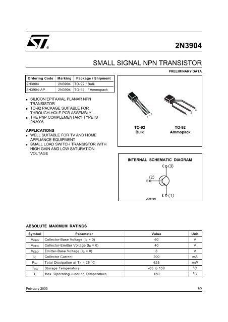
®<strong>2N3904</strong>SMALL SIGNAL NPN TRANSISTORPRELIMINARY DATAOrdering Code Marking Package / Shipment<strong>2N3904</strong> <strong>2N3904</strong> TO-92 / Bulk<strong>2N3904</strong>-AP <strong>2N3904</strong> TO-92 / Ammopack■■■SILICON EPITAXIAL PLANAR NPNTRANSISTORTO-92 PACKAGE SUITABLE FORTHROUGH-HOLE PCB ASSEMBLYTHE PNP COMPLEMENTARY TYPE IS2N3906APPLICATIONS■ WELL SUITABLE FOR TV AND HOMEAPPLIANCE EQUIPMENT■ SMALL LOAD SWITCH TRANSISTOR WITHHIGH GAIN AND LOW SATURATIONVOLTAGETO-92BulkTO-92AmmopackINTERNAL SCHEMATIC DIAGRAMABSOLUTE MAXIMUM RATINGSSymbol Parameter Value UnitV CBO Collector-Base Voltage (I E = 0) 60 VV CEO Collector-Emitter Voltage (I B = 0) 40 VV EBO Emitter-Base Voltage (I C = 0) 6 VI C Collector Current 200 mAPtot Total Dissipation at TC = 25 o C 625 mWT stg Storage Temperature -65 to 150T j Max. Operating Junction Temperature 150o Co CFebruary 20031/5
<strong>2N3904</strong>THERMAL DATAR thj-amb •Rthj-case •Thermal Resistance Junction-AmbientThermal Resistance Junction-CaseMaxMax20083.3o C/Wo C/WELECTRICAL CHARACTERISTICS (T case = 25 o C unless otherwise specified)Symbol Parameter Test Conditions Min. Typ. Max. UnitICEX Collector Cut-off VCE = 30 V 50 nACurrent (V BE = -3 V)I BEX Base Cut-off Current(V BE = -3 V)V CE = 30 V 50 nAV (BR)CEO∗V (BR)CBOV(BR)EBOV CE(sat)∗V BE(sat)∗Collector-EmitterBreakdown Voltage(I B = 0)Collector-BaseBreakdown Voltage(I E = 0)Emitter-BaseBreakdown Voltage(I C = 0)Collector-EmitterSaturation VoltageI C = 1 mA 40 VI C = 10 µA 60 VI E = 10 µA 6 VI C = 10 mAIC = 50 mAI B = 1 mAIB = 5 mABase-EmitterSaturation VoltageI C = 10 mA I B = 1 mAh FE∗ DC Current Gain I C = 0.1 mA V CE = 1 VI C = 1 mA V CE = 1 VI C = 10 mA V CE = 1 VI C = 50 mA V CE = 1 VIC = 100 mA VCE = 1 VI C = 50 mA I B = 5 mA 0.65608010060300.20.20.850.95f T Transition Frequency I C = 10 mA V CE = 20 V f = 100 MHz 250 270 MHzCollector-BaseIE = 0 VCB = 10 V f = 1 MHz 4 pFCapacitanceEmitter-BaseIC = 0 VEB = 0.5 V f = 1 MHz 18 pFCapacitanceNF Noise Figure V CE = 5 V I C = 0.1 mA f = 10 Hz5 dBto 15.7 KHz R G = 1 KΩCCBOCEBOt dtrt st fDelay TimeRise TimeStorage TimeFall TimeI C = 10 mAVCC = 30 VI C = 10 mAV CC = 30 V∗ Pulsed: Pulse duration = 300 µs, duty cycle ≤ 2 %I B = 1 mAI B1 = -I B2 = 1 mA300353520050VVVVnsnsnsns2/5
<strong>2N3904</strong>TO-92 MECHANICAL DATADIM.mminchMIN. TYP. MAX. MIN. TYP. MAX.A 4.32 4.95 0.170 0.195b 0.36 0.51 0.014 0.020D 4.45 4.95 0.175 0.194E 3.30 3.94 0.130 0.155e 2.41 2.67 0.095 0.105e1 1.14 1.40 0.045 0.055L 12.70 15.49 0.500 0.609R 2.16 2.41 0.085 0.094S1 1.14 1.52 0.045 0.059W 0.41 0.56 0.016 0.022V 4 degree 6 degree 4 degree 6 degree3/5
<strong>2N3904</strong>TO-92 AMMOPACK SHIPMENT (Suffix"-AP") MECHANICAL DATADIM.mminchMIN. TYP. MAX. MIN. TYP. MAX.A1 4.80 0.189T 3.80 0.150T1 1.60 0.063T2 2.30 0.091d 0.48 0.019P0 12.50 12.70 12.90 0.492 0.500 0.508P2 5.65 6.35 7.05 0.222 0.250 0.278F1,F2 2.44 2.54 2.94 0.096 0.100 0.116delta H -2.00 2.00 -0.079 0.079W 17.50 18.00 19.00 0.689 0.709 0.748W0 5.70 6.00 6.30 0.224 0.236 0.248W1 8.50 9.00 9.25 0.335 0.354 0.364W2 0.50 0.020H 18.50 20.50 0.728 0.807H0 15.50 16.00 16.50 0.610 0.630 0.650H1 25.00 0.984D0 3.80 4.00 4.20 0.150 0.157 0.165t 0.90 0.035L 11.00 0.433I1 3.00 0.118delta P -1.00 1.00 -0.039 0.0394/5
<strong>2N3904</strong>Information furnished is believed to be accurate and reliable. However, STMicroelectronics assumes no responsibility for the consequencesof use of such information nor for any infringement of patents or other rights of third parties which may result from its use. No license isgranted by implication or otherwise under any patent or patent rights of STMicroelectronics. Specification mentioned in this publication aresubject to change without notice. This publication supersedes and replaces all information previously supplied. STMicroelectronics productsare not authorized for use as critical components in life support devices or systems without express written approval of STMicroelectronics.The ST logo is a trademark of STMicroelectronics© 2003 STMicroelectronics – Printed in Italy – All Rights ReservedSTMicroelectronics GROUP OF COMPANIESAustralia - Brazil - Canada - China - Finland - France - Germany - Hong Kong - India - Israel - Italy - Japan - Malaysia - Malta - Morocco -Singapore - Spain - Sweden - Switzerland - United Kingdom - United States.http://www.st.com5/5