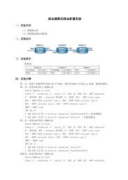
Dual 2/4Line Decoders
Dual 2/4Line Decoders
Dual 2/4Line Decoders

You also want an ePaper? Increase the reach of your titles
YUMPU automatically turns print PDFs into web optimized ePapers that Google loves.
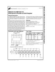
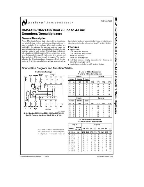
DM54155DM74155 <strong>Dual</strong> 2-Line to 4-Line<strong>Decoders</strong>DemultiplexersGeneral DescriptionThese TTL circuits feature dual 1-line-to-4-line demultiplexerswith individual strobes and common binary-address inputsin a single 16-pin package When both sections areenabled by the strobes the common address inputs sequentiallyselect and route associated input data to the appropriateoutput of each section The individual strobes permitactivating or inhibiting each of the 4-bit sections as desiredData applied to input C1 is inverted at its outputs anddata applied at C2 is true through its outputs The inverterfollowing the C1 data input permits use as a 3-to-8-line decoderor 1-to-8-line demultiplexer without external gatingConnection Diagram and Function Tables<strong>Dual</strong>-In-Line PackageTLF6549–1Order Number DM54155J DM54155W or DM74155NSee NS Package Number J16A N16A or W16AFebruary 1993Input clamping diodes are provided on these circuits to minimizetransmission-line effects and simplify system designFeaturesYYYApplications<strong>Dual</strong> 2-to-4-line decoder<strong>Dual</strong> 1-to-4-line demultiplexer3-to-8-line decoder1-to-8-line demultiplexerIndividual strobes simplify cascading for decoding ordemultiplexing larger wordsInput clamping diodes simplify system design2-Line-to-4-Line Decoder or1-Line-to-4-Line DemultiplexerInputsOutputsSelect Strobe DataB A G1 C1 1Y0 1Y1 1Y2 1Y3X X H X H H H HL L L H L H H HL H L H H L H HH L L H H H L HH H L H H H H LX X X L H H H HInputsOutputsSelect Strobe DataB A G2 C2 2Y0 2Y1 2Y2 2Y3X X H X H H H HL L L L L H H HL H L L H L H HH L L L H H L HH H L L H H H LX X X H H H H HDM54155DM74155 <strong>Dual</strong> 2-Line to 4-Line <strong>Decoders</strong>Demultiplexers3-Line-to-8-Line Decoder or1-Line-to-8-Line DemultiplexerInputsOutputsC e inputs C1 and C2 connected togetherG e inputs G1 and G2 connected togetherH e high level L e low level X e don’t careSelectStrobe (0) (1) (2) (3) (4) (5) (6) (7)Or DataC B A G 2Y0 2Y1 2Y2 2Y3 1Y0 1Y1 1Y2 1Y3X X X H H H H H H H H HL L L L L H H H H H H HL L H L H L H H H H H HL H L L H H L H H H H HL H H L H H H L H H H HH L L L H H H H L H H HH L H L H H H H H L H HH H L L H H H H H H L HH H H L H H H H H H H LC1995 National Semiconductor CorporationTLF6549RRD-B30M105Printed in U S A
Absolute Maximum Ratings (Note)If MilitaryAerospace specified devices are requiredplease contact the National Semiconductor SalesOfficeDistributors for availability and specificationsSupply Voltage7VInput Voltage55VOperating Free Air Temperature RangeDM54b55Ctoa125CDM740Ctoa70CStorage Temperature Rangeb65Ctoa150CRecommended Operating ConditionsSymbolParameterNote The ‘‘Absolute Maximum Ratings’’ are those valuesbeyond which the safety of the device cannot be guaranteedThe device should not be operated at these limits Theparametric values defined in the ‘‘Electrical Characteristics’’table are not guaranteed at the absolute maximum ratingsThe ‘‘Recommended Operating Conditions’’ table will definethe conditions for actual device operationDM54155DM74155Min Nom Max Min Nom MaxV CC Supply Voltage 45 5 55 475 5 525 VV IH High Level Input Voltage 2 2 VV IL Low Level Input Voltage 08 08 VI OH High Level Output Current b08 b08 mAI OL Low Level Output Current 16 16 mAT A Free Air Operating Temperature b55 125 0 70 CElectrical Characteristics over recommended operating free air temperature range (unless otherwise noted)Symbol Parameter Conditions MinTyp(Note 1)V I Input Clamp Voltage V CC eMin I I eb12 mA b15 VV OH High Level Output V CC e Min I OH e MaxVoltageV IL e Max V IH e MinV OL Low Level Output V CC e Min I OL e MaxVoltageV IH e Min V IL e MaxI I Input Current Max V CC e Max V I e 55VInput Voltage24Max04UnitsUnitsVV1 mAI IH High Level Input Current V CC e Max V I e 24V 40 mAI IL Low Level Input Current V CC e Max V I e 04V b16 mAI OS Short Circuit V CC e Max DM54 b20 b55 mAOutput Current (Note 2)DM74 b18 b55I CC Supply Current V CC e Max DM54 25 35 mA(Note 3)DM74 25 40Note 1 All typicals are at V CC e 5V T A e 25CNote 2 Not more than one output should be shorted at a timeNote 3 I CC is measured with the outputs open A B and C1 inputs at 45V and C2 G1 and G2 inputs grounded2
Switching Characteristics at V CC e 5V and T A e 25C (See Section 1 for Test Waveforms and Output Load)SymbolParameterFrom (Input)To (Output)t PLH Propagation Delay Time A B C2 G1Low to High Level Outputor G2 to Yt PHL Propagation Delay Time A B C2 G1High to Low Level Outputor G2 to Yt PLH Propagation Delay Time A or BLow to High Level Outputto Yt PHL Propagation Delay Time A or BHigh to Low Level Outputto Yt PLH Propagation Delay Time C1Low to High Level Outputto Yt PHL Propagation Delay Time C1High to Low Level Outputto YR L e 400XC L e15 pFUnitsMinMax20 ns27 ns32 ns32 ns24 ns27 nsLogic DiagramTLF6549–23
Physical Dimensions inches (millimeters)16-Lead Ceramic <strong>Dual</strong>-In-Line Package (J)Order Number DM54155JNS Package Number J16A16-Lead Molded <strong>Dual</strong>-In-Line Package (N)Order Number DM74155NNS Package Number N16E5
DM54155DM74155 <strong>Dual</strong> 2-Line to 4-Line <strong>Decoders</strong>DemultiplexersPhysical Dimensions inches (millimeters) (Continued)16-Lead Ceramic Flat Package (W)Order Number DM54155WNS Package Number W16ALIFE SUPPORT POLICYNATIONAL’S PRODUCTS ARE NOT AUTHORIZED FOR USE AS CRITICAL COMPONENTS IN LIFE SUPPORTDEVICES OR SYSTEMS WITHOUT THE EXPRESS WRITTEN APPROVAL OF THE PRESIDENT OF NATIONALSEMICONDUCTOR CORPORATION As used herein1 Life support devices or systems are devices or 2 A critical component is any component of a lifesystems which (a) are intended for surgical implant support device or system whose failure to perform caninto the body or (b) support or sustain life and whose be reasonably expected to cause the failure of the lifefailure to perform when properly used in accordance support device or system or to affect its safety orwith instructions for use provided in the labeling can effectivenessbe reasonably expected to result in a significant injuryto the userNational Semiconductor National Semiconductor National Semiconductor National SemiconductorCorporation Europe Hong Kong Ltd Japan Ltd1111 West Bardin Road Fax (a49) 0-180-530 85 86 13th Floor Straight Block Tel 81-043-299-2309Arlington TX 76017 Email cnjwge tevm2nsccom Ocean Centre 5 Canton Rd Fax 81-043-299-2408Tel 1(800) 272-9959 Deutsch Tel (a49) 0-180-530 85 85 Tsimshatsui KowloonFax 1(800) 737-7018 English Tel (a49) 0-180-532 78 32 Hong KongFranais Tel (a49) 0-180-532 93 58 Tel (852) 2737-1600Italiano Tel (a49) 0-180-534 16 80 Fax (852) 2736-9960National does not assume any responsibility for use of any circuitry described no circuit patent licenses are implied and National reserves the right at any time without notice to change said circuitry and specifications