CNY70 Datasheet - Vishay
CNY70 Datasheet - Vishay
CNY70 Datasheet - Vishay
- No tags were found...

You also want an ePaper? Increase the reach of your titles
YUMPU automatically turns print PDFs into web optimized ePapers that Google loves.
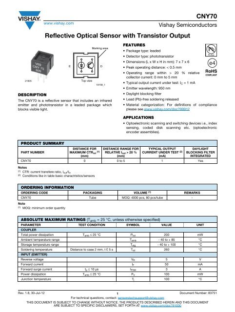
www.vishay.com<strong>CNY70</strong><strong>Vishay</strong> SemiconductorsReflective Optical Sensor with Transistor Output21835DESCRIPTIONThe <strong>CNY70</strong> is a reflective sensor that includes an infraredemitter and phototransistor in a leaded package whichblocks visible light.ETop viewMarking areaD19158_1FEATURES• Package type: leaded• Detector type: phototransistor• Dimensions (L x W x H in mm): 7 x 7 x 6• Peak operating distance: < 0.5 mm• Operating range within > 20 % relativecollector current: 0 mm to 5 mm• Typical output current under test: I C = 1 mA• Emitter wavelength: 950 nm• Daylight blocking filter• Lead (Pb)-free soldering released• Material categorization: For definitions of complianceplease see www.vishay.com/doc?99912APPLICATIONS• Optoelectronic scanning and switching devices i.e., indexsensing, coded disk scanning etc. (optoelectronicencoder assemblies).PRODUCT SUMMARYPART NUMBERDISTANCE FORMAXIMUM CTR rel (1)(mm)Notes(1) CTR: current transfere ratio, I out /I in(2) Conditions like in table basic charactristics/sensorsDISTANCE RANGE FORRELATIVE I out > 20 %(mm)TYPICAL OUTPUTCURRENT UNDER TEST (2)(mA)DAYLIGHTBLOCKING FILTERINTEGRATED<strong>CNY70</strong> 0 0 to 5 1 YesORDERING INFORMATIONORDERING CODE PACKAGING VOLUME (1) REMARKS<strong>CNY70</strong> Tube MOQ: 4000 pcs, 80 pcs/tube -Note(1) MOQ: minimum order quantityABSOLUTE MAXIMUM RATINGS (T amb = 25 °C, unless otherwise specified)PARAMETER TEST CONDITION SYMBOL VALUE UNITCOUPLERTotal power dissipation T amb ≤ 25 °C P tot 200 mWAmbient temperature range T amb - 40 to + 85 °CStorage temperature range T stg - 40 to + 100 °CSoldering temperature Distance to case 2 mm, t £ 5 s T sd 260 °CINPUT (EMITTER)Reverse voltage V R 5 VForward current I F 50 mAForward surge current t p ≤ 10 μs I FSM 3 APower dissipation T amb ≤ 25 °C P V 100 mWJunction temperature T j 100 °CRev. 1.8, 30-Jul-12 1 Document Number: 83751For technical questions, contact: sensorstechsupport@vishay.comTHIS DOCUMENT IS SUBJECT TO CHANGE WITHOUT NOTICE. THE PRODUCTS DESCRIBED HEREIN AND THIS DOCUMENTARE SUBJECT TO SPECIFIC DISCLAIMERS, SET FORTH AT www.vishay.com/doc?91000
www.vishay.com<strong>CNY70</strong><strong>Vishay</strong> SemiconductorsABSOLUTE MAXIMUM RATINGS (T amb = 25 °C, unless otherwise specified)PARAMETER TEST CONDITION SYMBOL VALUE UNITOUTPUT (DETECTOR)Collector emitter voltage V CEO 32 VEmitter collector voltage V ECO 7 VCollector current I C 50 mAPower dissipation T amb ≤ 25 °C P V 100 mWJunction temperature T j 100 °CABSOLUTE MAXIMUM RATINGS300P - Power Dissipation (mW)200100Coupled devicePhototransistorIR - diode95 110710025 50 75 100T amb - Ambient Temperature (°C)Fig. 1 - Power Dissipation vs. Ambient TemperatureBASIC CHARACTERISTICS (T amb = 25 °C, unless otherwise specified)PARAMETER TEST CONDITION SYMBOL MIN. TYP. MAX. UNITCOUPLERVCollector currentCE = 5 V, I F = 20 mA,Id = 0.3 mm (figure 1)(2) C 0.3 1.0 mACross talk current V CE = 5 V, I F = 20 mA, (figure 2) I (3) CX 600 nACollector emitter saturationvoltageI F = 20 mA, I C = 0.1 mA,d = 0.3 mm (figure 1)Notes(1) Measured with the “Kodak neutral test card”, white side with 90 % diffuse reflectance(2) Measured without reflecting mediumV CEsat (2) 0.3 VINPUT (EMITTER)Forward voltage I F = 50 mA V F 1.25 1.6 VRadiant intensity I F = 50 mA, t p = 20 ms I e 7.5 mW/srPeak wavelength I F = 100 mA λ P 940 nmVirtual source diameter Method: 63 % encircled energy d 1.2 mmOUTPUT (DETECTOR)Collector emitter voltage I C = 1 mA V CEO 32 VEmitter collector voltage I E = 100 μA V ECO 5 VCollector dark current V CE = 20 V, I F = 0 A, E = 0 lx I CEO 200 nARev. 1.8, 30-Jul-12 2 Document Number: 83751For technical questions, contact: sensorstechsupport@vishay.comTHIS DOCUMENT IS SUBJECT TO CHANGE WITHOUT NOTICE. THE PRODUCTS DESCRIBED HEREIN AND THIS DOCUMENTARE SUBJECT TO SPECIFIC DISCLAIMERS, SET FORTH AT www.vishay.com/doc?91000
www.vishay.com<strong>CNY70</strong><strong>Vishay</strong> SemiconductorsReflecting medium(Kodak neutral test card)d~ ~~~ ~~DetectorEmitterA C E CFig. 2 - Test Condition95 10893BASIC CHARACTERISTICS (T amb = 25 °C, unless otherwise specified)I F - Forward Current (mA)1000100101I - Collector Current (mA)C1010.10.01Kodak neutral card(white side)d = 0.3 mmV CE = 5 V96 118620.100.4 0.8 1.2 1.6 2.0V F - Forward Voltage (V)Fig. 3 - Forward Current vs. Forward Voltage0.0010.195 110651I F - Forward Current (mA)Fig. 5 - Collector Current vs. Forward Current10100CTR rel - Relative Current Transfer Ratio96 119131.51.4 VCE= 5 V1.3 I = 20 mAF1.2 d = 0.3 mm1.11.00.90.80.70.60.5- 30 - 20 -10 0 10 20 30 40 50 60 70 80T amb - Ambient Temperature (°C)I - Collector Current (mA)C1010.10.01Kodak neutral card(white side)d = 0.3 mmI F = 50 mA20 mA10 mA5 mA2 mA1 mA0.0010.111095 11066 V CE - Collector Emitter Voltage (V)100Fig. 4 - Relative Current Transfer Ratio vs. Ambient TemperatureFig. 6 - Collector Current vs. Collector Emitter VoltageRev. 1.8, 30-Jul-12 3 Document Number: 83751For technical questions, contact: sensorstechsupport@vishay.comTHIS DOCUMENT IS SUBJECT TO CHANGE WITHOUT NOTICE. THE PRODUCTS DESCRIBED HEREIN AND THIS DOCUMENTARE SUBJECT TO SPECIFIC DISCLAIMERS, SET FORTH AT www.vishay.com/doc?91000
www.vishay.com<strong>CNY70</strong><strong>Vishay</strong> SemiconductorsCTR - Current Transfer Ratio (%)100101Kodak neutral card(white side)d = 0.3 mmV CE =5VI - Collector Current (mA)C1010.1V CE = 5 VI F = 20 mAd0.10.1110 10096 11914 I F - Forward Current (mA)Fig. 7 - Current Transfer Ratio vs. Forward Current0.001095 1106924d - Distance (mm)Fig. 9 - Collector Current vs. Distance6810CTR - Current Transfer Ratio (%)10196 120012 mAI F = 50 mA20 mA10 mA5 mA1 mAKodak neutral card(white side)d = 0.3 mm0.10.1 1 10 100V CE - Collector Emitter Voltage (V)I erel - Relative Radiant IntensityI crel - Relative Collector Current95 110631.00.90.80.70.60.40.20°010° 20°0.20.430°40°50°60°70°80°0.6Fig. 8 - Current Transfer Ratio vs. Collector Emitter VoltageFig. 10 - Relative Radiant Intensity/Collector Current vs.Angular Displacement1.0I Crel - Relative Collector Current0.90.80.70.60.50.40.30.20.1d = 5 mm4 mm3 mm2 mm1 mm0V CE = 5 VI F = 20 mA1.5E DdEDss05 mm10 mm05 mm10 mm0.00123456789101196 11915s - Displacement (mm)Fig. 11 - Relative Collector Current vs. DisplacementRev. 1.8, 30-Jul-12 4 Document Number: 83751For technical questions, contact: sensorstechsupport@vishay.comTHIS DOCUMENT IS SUBJECT TO CHANGE WITHOUT NOTICE. THE PRODUCTS DESCRIBED HEREIN AND THIS DOCUMENTARE SUBJECT TO SPECIFIC DISCLAIMERS, SET FORTH AT www.vishay.com/doc?91000
www.vishay.com<strong>CNY70</strong><strong>Vishay</strong> SemiconductorsPACKAGE DIMENSIONS in millimeters95 11345TUBE DIMENSIONS in millimeters20291Rev. 1.8, 30-Jul-12 5 Document Number: 83751For technical questions, contact: sensorstechsupport@vishay.comTHIS DOCUMENT IS SUBJECT TO CHANGE WITHOUT NOTICE. THE PRODUCTS DESCRIBED HEREIN AND THIS DOCUMENTARE SUBJECT TO SPECIFIC DISCLAIMERS, SET FORTH AT www.vishay.com/doc?91000
Packaging and Ordering InformationPackaging and Ordering Information<strong>Vishay</strong> SemiconductorsPART NUMBER MOQ (1) PCS PER TUBENotes(1) MOQ: minimum order quantity(2) Please refer to datasheetsTUBE SPECIFICATION FIGURESTUBE SPEC.(FIGURE)CONSTITUENTS(FORMS)<strong>CNY70</strong> 4000 80 1 28TCPT1300X01 2000 Reel (2) 29TCRT1000 1000 Bulk - 26TCRT1010 1000 Bulk - 26TCRT5000 4500 50 2 27TCRT5000L 2400 48 3 27TCST1030 5200 65 5 24TCST1030L 2600 65 6 24TCST1103 1020 85 4 24TCST1202 1020 85 4 24TCST1230 4800 60 7 24TCST1300 1020 85 4 24TCST2103 1020 85 4 24TCST2202 1020 85 4 24TCST2300 1020 85 4 24TCST5250 4860 30 8 24TCUT1300X01 2000 Reel (2) 29TCZT8020-PAER 2500 Bulk - 2215198Fig. 1Document Number: 80112 For technical questions, contact: optocoupleranswers@vishay.com www.vishay.comRev. 1.1, 02-Jul-09 1
Packaging and Ordering Information<strong>Vishay</strong> Semiconductors Packaging and Ordering Information15210Fig. 215201Fig. 3www.vishay.com For technical questions, contact: optocoupleranswers@vishay.com Document Number: 801122 Rev. 1.1, 02-Jul-09
Packaging and Ordering InformationPackaging and Ordering Information<strong>Vishay</strong> Semiconductors15199Fig. 4Fig. 515202Document Number: 80112 For technical questions, contact: optocoupleranswers@vishay.com www.vishay.comRev. 1.1, 02-Jul-09 3
Packaging and Ordering Information<strong>Vishay</strong> Semiconductors Packaging and Ordering Information15196Fig. 615195Fig. 7www.vishay.com For technical questions, contact: optocoupleranswers@vishay.com Document Number: 801124 Rev. 1.1, 02-Jul-09
Packaging and Ordering InformationPackaging and Ordering Information<strong>Vishay</strong> Semiconductors20257Fig. 8Document Number: 80112 For technical questions, contact: optocoupleranswers@vishay.com www.vishay.comRev. 1.1, 02-Jul-09 5
www.vishay.comLegal Disclaimer Notice<strong>Vishay</strong>DisclaimerALL PRODUCT, PRODUCT SPECIFICATIONS AND DATA ARE SUBJECT TO CHANGE WITHOUT NOTICE TO IMPROVERELIABILITY, FUNCTION OR DESIGN OR OTHERWISE.<strong>Vishay</strong> Intertechnology, Inc., its affiliates, agents, and employees, and all persons acting on its or their behalf (collectively,“<strong>Vishay</strong>”), disclaim any and all liability for any errors, inaccuracies or incompleteness contained in any datasheet or in any otherdisclosure relating to any product.<strong>Vishay</strong> makes no warranty, representation or guarantee regarding the suitability of the products for any particular purpose orthe continuing production of any product. To the maximum extent permitted by applicable law, <strong>Vishay</strong> disclaims (i) any and allliability arising out of the application or use of any product, (ii) any and all liability, including without limitation special,consequential or incidental damages, and (iii) any and all implied warranties, including warranties of fitness for particularpurpose, non-infringement and merchantability.Statements regarding the suitability of products for certain types of applications are based on <strong>Vishay</strong>’s knowledge of typicalrequirements that are often placed on <strong>Vishay</strong> products in generic applications. Such statements are not binding statementsabout the suitability of products for a particular application. It is the customer’s responsibility to validate that a particularproduct with the properties described in the product specification is suitable for use in a particular application. Parametersprovided in datasheets and/or specifications may vary in different applications and performance may vary over time. Alloperating parameters, including typical parameters, must be validated for each customer application by the customer’stechnical experts. Product specifications do not expand or otherwise modify <strong>Vishay</strong>’s terms and conditions of purchase,including but not limited to the warranty expressed therein.Except as expressly indicated in writing, <strong>Vishay</strong> products are not designed for use in medical, life-saving, or life-sustainingapplications or for any other application in which the failure of the <strong>Vishay</strong> product could result in personal injury or death.Customers using or selling <strong>Vishay</strong> products not expressly indicated for use in such applications do so at their own risk. Pleasecontact authorized <strong>Vishay</strong> personnel to obtain written terms and conditions regarding products designed for such applications.No license, express or implied, by estoppel or otherwise, to any intellectual property rights is granted by this document or byany conduct of <strong>Vishay</strong>. Product names and markings noted herein may be trademarks of their respective owners.Material Category Policy<strong>Vishay</strong> Intertechnology, Inc. hereby certifies that all its products that are identified as RoHS-Compliant fulfill thedefinitions and restrictions defined under Directive 2011/65/EU of The European Parliament and of the Councilof June 8, 2011 on the restriction of the use of certain hazardous substances in electrical and electronic equipment(EEE) - recast, unless otherwise specified as non-compliant.Please note that some <strong>Vishay</strong> documentation may still make reference to RoHS Directive 2002/95/EC. We confirm thatall the products identified as being compliant to Directive 2002/95/EC conform to Directive 2011/65/EU.<strong>Vishay</strong> Intertechnology, Inc. hereby certifies that all its products that are identified as Halogen-Free follow Halogen-Freerequirements as per JEDEC JS709A standards. Please note that some <strong>Vishay</strong> documentation may still make referenceto the IEC 61249-2-21 definition. We confirm that all the products identified as being compliant to IEC 61249-2-21conform to JEDEC JS709A standards.Revision: 02-Oct-12 1 Document Number: 91000