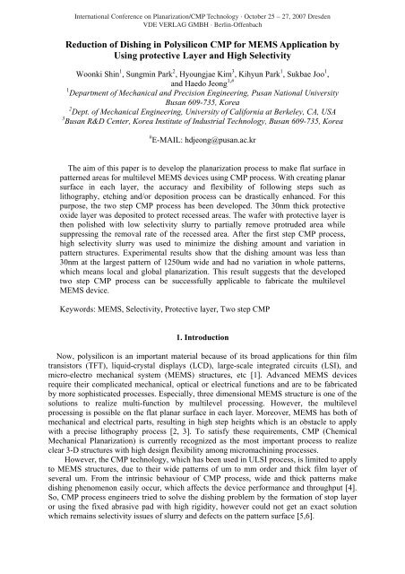
Reduction of Dishing in Polysilicon CMP for MEMS Application by ...
Reduction of Dishing in Polysilicon CMP for MEMS Application by ...
Reduction of Dishing in Polysilicon CMP for MEMS Application by ...
- No tags were found...

Create successful ePaper yourself
Turn your PDF publications into a flip-book with our unique Google optimized e-Paper software.
International Conference on Planarization/<strong>CMP</strong> Technology · October 25 – 27, 2007 DresdenVDE VERLAG GMBH · Berl<strong>in</strong>-Offenbach<strong>Reduction</strong> <strong>of</strong> <strong>Dish<strong>in</strong>g</strong> <strong>in</strong> <strong>Polysilicon</strong> <strong>CMP</strong> <strong>for</strong> <strong>MEMS</strong> <strong>Application</strong> <strong>by</strong>Us<strong>in</strong>g protective Layer and High SelectivityWoonki Sh<strong>in</strong> 1 , Sungm<strong>in</strong> Park 2 , Hyoungjae Kim 3 , Kihyun Park 1 , Sukbae Joo 1 ,and Haedo Jeong 1,#1 Department <strong>of</strong> Mechanical and Precision Eng<strong>in</strong>eer<strong>in</strong>g, Pusan National UniversityBusan 609-735, Korea2 Dept. <strong>of</strong> Mechanical Eng<strong>in</strong>eer<strong>in</strong>g, University <strong>of</strong> Cali<strong>for</strong>nia at Berkeley, CA, USA3 Busan R&D Center, Korea Institute <strong>of</strong> Industrial Technology, Busan 609-735, Korea# E-MAIL: hdjeong@pusan.ac.krThe aim <strong>of</strong> this paper is to develop the planarization process to make flat surface <strong>in</strong>patterned areas <strong>for</strong> multilevel <strong>MEMS</strong> devices us<strong>in</strong>g <strong>CMP</strong> process. With creat<strong>in</strong>g planarsurface <strong>in</strong> each layer, the accuracy and flexibility <strong>of</strong> follow<strong>in</strong>g steps such aslithography, etch<strong>in</strong>g and/or deposition process can be drastically enhanced. For thispurpose, the two step <strong>CMP</strong> process has been developed. The 30nm thick protectiveoxide layer was deposited to protect recessed areas. The wafer with protective layer isthen polished with low selectivity slurry to partially remove protruded area whilesuppress<strong>in</strong>g the removal rate <strong>of</strong> the recessed area. After the first step <strong>CMP</strong> process,high selectivity slurry was used to m<strong>in</strong>imize the dish<strong>in</strong>g amount and variation <strong>in</strong>pattern structures. Experimental results show that the dish<strong>in</strong>g amount was less than30nm at the largest pattern <strong>of</strong> 1250um wide and had no variation <strong>in</strong> whole patterns,which means local and global planarization. This result suggests that the developedtwo step <strong>CMP</strong> process can be successfully applicable to fabricate the multilevel<strong>MEMS</strong> device.Keywords: <strong>MEMS</strong>, Selectivity, Protective layer, Two step <strong>CMP</strong>1. IntroductionNow, polysilicon is an important material because <strong>of</strong> its broad applications <strong>for</strong> th<strong>in</strong> filmtransistors (TFT), liquid-crystal displays (LCD), large-scale <strong>in</strong>tegrated circuits (LSI), andmicro-electro mechanical system (<strong>MEMS</strong>) structures, etc [1]. Advanced <strong>MEMS</strong> devicesrequire their complicated mechanical, optical or electrical functions and are to be fabricated<strong>by</strong> more sophisticated processes. Especially, three dimensional <strong>MEMS</strong> structure is one <strong>of</strong> thesolutions to realize multi-function <strong>by</strong> multilevel process<strong>in</strong>g. However, the multilevelprocess<strong>in</strong>g is possible on the flat planar surface <strong>in</strong> each layer. Moreover, <strong>MEMS</strong> has both <strong>of</strong>mechanical and electrical parts, result<strong>in</strong>g <strong>in</strong> high step heights which is an obstacle to applywith a precise lithography process [2, 3]. To satisfy these requirements, <strong>CMP</strong> (ChemicalMechanical Planarization) is currently recognized as the most important process to realizeclear 3-D structures with high design flexibility among micromach<strong>in</strong><strong>in</strong>g processes.However, the <strong>CMP</strong> technology, which has been used <strong>in</strong> ULSI process, is limited to applyto <strong>MEMS</strong> structures, due to their wide patterns <strong>of</strong> um to mm order and thick film layer <strong>of</strong>several um. From the <strong>in</strong>tr<strong>in</strong>sic behaviour <strong>of</strong> <strong>CMP</strong> process, wide and thick patterns makedish<strong>in</strong>g phenomenon easily occur, which affects the device per<strong>for</strong>mance and throughput [4].So, <strong>CMP</strong> process eng<strong>in</strong>eers tried to solve the dish<strong>in</strong>g problem <strong>by</strong> the <strong>for</strong>mation <strong>of</strong> stop layeror us<strong>in</strong>g the fixed abrasive pad with high rigidity, however could not get an exact solutionwhich rema<strong>in</strong>s selectivity issues <strong>of</strong> slurry and defects on the pattern surface [5,6].
International Conference on Planarization/<strong>CMP</strong> Technology · October 25 – 27, 2007 DresdenVDE VERLAG GMBH · Berl<strong>in</strong>-OffenbachThis paper focuses on the realization <strong>of</strong> local and global planarization <strong>of</strong> polysilicon<strong>MEMS</strong> structures <strong>by</strong> reduc<strong>in</strong>g the dish<strong>in</strong>g amount and its variation. The basic processmechanism is two step polish<strong>in</strong>g with different selectivity slurries on the protective orsacrificial oxide layer.Table 1 Specifications <strong>of</strong> the used slurry <strong>in</strong> the experimentSlurry (Silica based) Sample A Sample B Sample CAbrasive type Fumed Colloidal ColloidalAbrasive size 175nm 70nm 12nmpH 10.8 12 10.9Concentration 13wt% 28wt% 30wt%<strong>Application</strong> SiO2 S<strong>in</strong>gle crystal Si Poly Si2. Experimental ConditionsThis paper focused on the prevention <strong>of</strong> dish<strong>in</strong>g problem generated <strong>in</strong> polysilicon patterns,which has been widely used <strong>in</strong> <strong>MEMS</strong> structures. Prior to <strong>in</strong>vestigat<strong>in</strong>g <strong>of</strong> dish<strong>in</strong>g reduction,three different types <strong>of</strong> slurry were used with vary<strong>in</strong>g abrasive types, concentrations and pHs<strong>of</strong> slurry <strong>in</strong> order to f<strong>in</strong>d out the selectivity between polysilicon and oxide(SiO 2 ) (Table 1).Especially, th<strong>in</strong> layer (
International Conference on Planarization/<strong>CMP</strong> Technology · October 25 – 27, 2007 DresdenVDE VERLAG GMBH · Berl<strong>in</strong>-Offenbachslurry with different selectivity on G&P POLI-500 polisher with endpo<strong>in</strong>t detection system.Fig. 1(a) shows the photo-mask <strong>of</strong> the test patterned wafer, which has various pattern sizes<strong>of</strong> polysilicon based on <strong>MEMS</strong> structure scales. Also, Fig. 1(b) and Fig. 1(c) show the opticalimages <strong>of</strong> “A” region and “B” region, respectively. The thickness pr<strong>of</strong>ile <strong>of</strong> patterned waferwas measured <strong>by</strong> us<strong>in</strong>g non-contact surface pr<strong>of</strong>iler, and the measur<strong>in</strong>g ranges are “A1-A2”and “B1-B2” as shown <strong>in</strong> Fig. 1(b) and (c), respectively.3. Results and DiscussionsFrom the basic experimental results, the selectivity <strong>of</strong> slurry A, B and C was found to be70:1~3:1, 235:1~30:1 and 120:1~135:1, respectively. In case <strong>of</strong> slurry B, its selectivity has awide control range and strongly depends on the change <strong>in</strong> SiO2 MRR. It hardly removes theoxide layer. The change <strong>in</strong> MRR seems to be orig<strong>in</strong>ated from the imbalance between thechemical and mechanical effects.Based on prelim<strong>in</strong>ary results, the polysilicon patterns with 100-1250um wide had beendirectly polished with oxide slurry at abrasive concentration <strong>of</strong> 13% (slurry A). The resultshowed not only a large dish<strong>in</strong>g amount, but also <strong>in</strong>creas<strong>in</strong>g dish<strong>in</strong>g amount accord<strong>in</strong>g topattern width (Fig. 2(a)). This experiment reveals that conventional <strong>CMP</strong> <strong>of</strong> polysilicon cannot planarize wide patterns <strong>for</strong> <strong>MEMS</strong> structures. To reduce the dish<strong>in</strong>g amount, authors havedeveloped two step <strong>CMP</strong> process (Fig. 2(b)) with the comb<strong>in</strong>ation <strong>of</strong> deposition <strong>of</strong> oxideprotective layer and us<strong>in</strong>g high selectivity <strong>CMP</strong> process. To realize this, th<strong>in</strong> protective layer<strong>of</strong> SiO2 (30nm) was deposited on top <strong>of</strong> polysilicon layer and the two step <strong>CMP</strong> wasimplemented <strong>by</strong> oxide <strong>CMP</strong> with slurry A followed <strong>by</strong> high selectivity <strong>CMP</strong> with slurry B.At the first step with low selectivity slurry A, the top area <strong>of</strong> protective layer was removed toexpose polysilicon layer while rema<strong>in</strong><strong>in</strong>g the protective layer <strong>in</strong> the trench. After remov<strong>in</strong>gthe protective layer, second step with high selectivity slurry was cont<strong>in</strong>ued down to thebottom <strong>of</strong> trench areas. Due to its high selectivity (235:1), the <strong>CMP</strong> process stoppedspontaneously at the bottom <strong>of</strong> the trench, which prevents dish<strong>in</strong>g <strong>in</strong> recessed areas.Direct <strong>CMP</strong> ProcessTwo Step <strong>CMP</strong> Process1) Poly-Si Deposition1) Protective Layer Deposition (30nm)2) Direct Poly-Si <strong>CMP</strong>2) First Step Oxide <strong>CMP</strong>SiO2Poly-Si3) Second Step Poly <strong>CMP</strong>Substrate4) BOE Strip <strong>of</strong> Oxide(a) conventional one step process(b) the developed two step processFig.2 <strong>Reduction</strong> <strong>of</strong> dish<strong>in</strong>g <strong>by</strong> us<strong>in</strong>g the two step <strong>CMP</strong> <strong>by</strong> the change <strong>of</strong> slurry selectivity
International Conference on Planarization/<strong>CMP</strong> Technology · October 25 – 27, 2007 DresdenVDE VERLAG GMBH · Berl<strong>in</strong>-Offenbach(a) be<strong>for</strong>e <strong>CMP</strong> (b) one step process (c) two step processFig. 3 Comparison <strong>of</strong> dish<strong>in</strong>g <strong>by</strong> one and two step processesThe comparison test <strong>of</strong> dish<strong>in</strong>g amount <strong>by</strong> one step and two step processes was per<strong>for</strong>med.Fig. 3 shows the <strong>in</strong><strong>for</strong>mation <strong>of</strong> surface pr<strong>of</strong>iles <strong>of</strong> 300um wide pattern trench which weremeasured <strong>by</strong> non-contact optical microscope. Fig.3(a) shows a pr<strong>of</strong>ile be<strong>for</strong>e <strong>CMP</strong>, and (b)shows the result <strong>of</strong> conventional one step <strong>CMP</strong> with large dish<strong>in</strong>g amount <strong>of</strong> 197nm, andf<strong>in</strong>ally (c) has an ideal result without dish<strong>in</strong>g, <strong>by</strong> the developed two step <strong>CMP</strong> process, whichverifies a successful trial that the th<strong>in</strong> layer <strong>of</strong> oxide protects poly-Si from high selectivityslurry.As <strong>for</strong> the uni<strong>for</strong>mity <strong>of</strong> dish<strong>in</strong>g amount, the one step process makes the dish<strong>in</strong>g amount<strong>in</strong>crease accord<strong>in</strong>g to pattern width. On the other hand, the two step process shows uni<strong>for</strong>mpr<strong>of</strong>iles without dish<strong>in</strong>g <strong>in</strong>dependent on the pattern width. Fig. 4 shows the surface pr<strong>of</strong>ilesafter one step and two step <strong>CMP</strong> accord<strong>in</strong>g to pattern <strong>of</strong> small (a) and large size (b). We canf<strong>in</strong>d the conventional one step <strong>CMP</strong> overcomes the requirement <strong>of</strong> <strong>MEMS</strong> structure up to300nm at the largest pattern width (1250um). However, the developed two step processenables an ideal uni<strong>for</strong>mity <strong>of</strong> dish<strong>in</strong>g amount, <strong>in</strong>dependent on the width <strong>of</strong> the patterntrenches, ma<strong>in</strong>ta<strong>in</strong><strong>in</strong>g constantly under 30nm.(a) small patterns(b) large patternsFig. 4 Pattern dependency <strong>of</strong> dish<strong>in</strong>g amount <strong>by</strong> one step and two step <strong>CMP</strong>There<strong>for</strong>e, the result shows the reduction per<strong>for</strong>mance <strong>of</strong> dish<strong>in</strong>g amount with less 30nm <strong>of</strong>dish<strong>in</strong>g even <strong>in</strong> 1250um trenched area (Fig. 5). Moreover, the two step process seems to be anexact solution to reduce the dish<strong>in</strong>g amount, regardless <strong>of</strong> the change <strong>of</strong> pattern width. Basedon polysilicon <strong>CMP</strong> results, we believe that a variety <strong>of</strong> pattern size can be successfully
International Conference on Planarization/<strong>CMP</strong> Technology · October 25 – 27, 2007 DresdenVDE VERLAG GMBH · Berl<strong>in</strong>-Offenbachplanarized <strong>by</strong> us<strong>in</strong>g developed two step process which also could be used to <strong>in</strong>creaseflexibility <strong>in</strong> design<strong>in</strong>g sophisticated <strong>MEMS</strong> devices.<strong>Dish<strong>in</strong>g</strong> amount (nm)4003503002502001501005001 step 2 step100 150 210 300 625 1250Pattern width (um)Fig. 5 Comparison <strong>of</strong> dish<strong>in</strong>g per<strong>for</strong>mance accord<strong>in</strong>g to pattern width4. ConclusionAs a <strong>MEMS</strong> device is gett<strong>in</strong>g sophisticated, advanced process has been developed to meetthe requirement <strong>of</strong> each process steps. One <strong>of</strong> the emerg<strong>in</strong>g needs <strong>for</strong> complicated <strong>MEMS</strong>device is to make multilevel <strong>MEMS</strong> structures to <strong>in</strong>clude more functions <strong>in</strong> smaller space. Torealize this requirement, planar surface is mandatory to stack multiple layers and the flatfoundation gives a lot <strong>of</strong> design flexibility <strong>for</strong> mak<strong>in</strong>g high per<strong>for</strong>mance devices.To make planar surface, the two step <strong>CMP</strong> process has been developed <strong>by</strong> us<strong>in</strong>g low andhigh selectivity slurry comb<strong>in</strong>ed with protective layer. The highest removal rate selectivitybetween polysilicon and oxide was 235:1 and the lowest selectivity was 3:1 depend<strong>in</strong>g ontypes <strong>of</strong> slurry. With two step approach, the achieved dish<strong>in</strong>g amount is suppressed to lessthan 30nm at 1250um trench. This result suggests that the developed <strong>CMP</strong> process can beapplicable <strong>for</strong> manufactur<strong>in</strong>g <strong>of</strong> multilevel <strong>MEMS</strong> devices with a variety <strong>of</strong> pattern size.References[1] A. Tanikawa and T. Tatsumi, J. Electrochem. Soc., Vol. 141, p.2848 (1994)[2] Levrecht von Trotha, George Moersch and Gerfried Zwicker, Advanced <strong>MEMS</strong>fabrication us<strong>in</strong>g <strong>CMP</strong>, Semiconductor International, (8/1/2004)[3] Jeffry J. Sniegowski, Chemical-mechanical polish<strong>in</strong>g: enhanc<strong>in</strong>g the manufacturability<strong>of</strong> <strong>MEMS</strong>, Proc. SPIE Vol. 2879, p. 104-115 (1996)[4] Beomyoung Park, et all, A Study on the <strong>Reduction</strong> <strong>of</strong> <strong>Dish<strong>in</strong>g</strong> and Erosion Defects <strong>in</strong>Tungsten <strong>CMP</strong>, J. <strong>of</strong> KSPE , Vol. 22, No. 2, p. 38-45 (2005)[5] Simon J. Fang, Vladimir A. Ukra<strong>in</strong>tsev, Control <strong>of</strong> <strong>Polysilicon</strong> Topography <strong>in</strong> a HighSelectivity <strong>CMP</strong> Process, J. Electrochem. Soc., Vol. 146, No. 3, p.1158-1162 (1999)[6] Hoyum Kim, Hoyongjae Kim and Haedo Jeong, Development <strong>of</strong> an AbrasiveEmbedded Pad <strong>for</strong> <strong>Dish<strong>in</strong>g</strong> <strong>Reduction</strong> and Uni<strong>for</strong>mity Enhancement, J. <strong>of</strong> KPS, Vol. 37,NO. 6, p. 945 (2000)