BD136/138/140 PNP Epitaxial Silicon Transistor
BD136/138/140 PNP Epitaxial Silicon Transistor
BD136/138/140 PNP Epitaxial Silicon Transistor
- No tags were found...

Create successful ePaper yourself
Turn your PDF publications into a flip-book with our unique Google optimized e-Paper software.
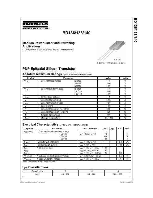
Medium Power Linear and SwitchingApplications• Complement to BD135, BD137 and BD139 respectively<strong>BD136</strong>/<strong>138</strong>/<strong>140</strong><strong>BD136</strong>/<strong>138</strong>/<strong>140</strong>1 TO-1261. Emitter 2.Collector 3.Base<strong>PNP</strong> <strong>Epitaxial</strong> <strong>Silicon</strong> <strong>Transistor</strong>Absolute Maximum Ratings T C =25°C unless otherwise notedSymbol Parameter Value UnitsV CBO Collector-Base Voltage : <strong>BD136</strong>: BD<strong>138</strong>: BD<strong>140</strong>V CEO Collector-Emitter Voltage : <strong>BD136</strong>: BD<strong>138</strong>: BD<strong>140</strong>V EBO Emitter-Base Voltage - 5 VI C Collector Current (DC) - 1.5 AI CP Collector Current (Pulse) - 3.0 AI B Base Current - 0.5 AP C Collector Dissipation (T C =25°C) 12.5 WP C Collector Dissipation (T a =25°C) 1.25 WT J Junction Temperature 150 °CT STG Storage Temperature - 55 ~ 150 °C- 45- 60- 80- 45- 60- 80VVVVVVElectrical Characteristics T C =25°C unless otherwise notedSymbol Parameter Test Condition Min. Typ. Max. UnitsV CEO (sus) * Collector-Emitter Sustaining Voltage: <strong>BD136</strong>: BD<strong>138</strong>: BD<strong>140</strong>I C = - 30mA, I B = 0 - 45- 60- 80VVVI CBO Collector Cut-off Current V CB = - 30V, I E = 0 - 0.1 µAI EBO Emitter Cut-off Current V EB = - 5V, I C = 0 - 10 µAh FE1 * DC Current Gain V CE = - 2V, I C = - 5mAh FE3 V CE = - 2V, I C = - 150mAh FE2V CE = - 2V, I C = - 0.5A* Pulse Test: PW=350µs, duty Cycle=2% Pulsedh FE Classificntion252540 250V CE (sat) * Collector-Emitter Saturation Voltage I C = - 500mA, I B = - 50mA - 0.5 VV BE (on) * Base-Emitter ON Voltage V CE = - 2V, I C = - 0.5A - 1 VClassification 6 10 16h FE3 40 ~ 100 63 ~ 160 100 ~ 250©2000 Fairchild Semiconductor International Rev. A, February 2000
Typical CharacteristicshFE, DC CURRENT GAIN100908070605040302010VCE = -2VVCE(sat)[mV], SATURATION VOLTAGE-500-450-400-350-300-250-200-150-100-50IC = 20 IBIC = 10 IB<strong>BD136</strong>/<strong>138</strong>/<strong>140</strong>0-10 -100 -1000IC[mA], COLLECTOR CURRENT-0-1E-3 -0.01 -0.1 -1 -10IC[A], COLLECTOR CURRENTFigure 1. DC current GainFigure 2. Collector-Emitter Saturation Voltage-1.1-10VBE[V], BASE-EMITTER VOLTAGE-1.0-0.9-0.8-0.7-0.6-0.5-0.4-0.3-0.2VBE(sat)IC = 10 IBVBE(on)VCE = -5VIC[A], COLLECTOR CURRENT-1-0.1IC MAX. (Pulsed)IC MAX. (Continuous)DC1ms100us<strong>BD136</strong>BD<strong>138</strong>10usBD<strong>140</strong>-0.1-1E-3 -0.01 -0.1 -1 -10IC[A], COLLECTOR CURRENT-0.01-1 -10 -100VCE[V], COLLECTOR-EMITTER VOLTAGEFigure 3. Base-Emitter VoltageFigure 4. Safe Operating Area20.017.5PC[W], POWER DISSIPATION15.012.510.07.55.02.50.00 25 50 75 100 125 150 175TC[ o C], CASE TEMPERATUREFigure 5. Power Derating©2000 Fairchild Semiconductor InternationalRev. A, February 2000
Package DemensionsTO-126<strong>BD136</strong>/<strong>138</strong>/<strong>140</strong>3.90 ±0.108.00 ±0.303.25 ±0.20ø3.20 ±0.1014.20MAX11.00 ±0.200.75 ±0.10(1.00)(0.50)1.60 ±0.100.75 ±0.1013.06 ±0.3016.10 ±0.201.75 ±0.202.28TYP[2.28±0.20]#12.28TYP[2.28±0.20]0.50 +0.10–0.05Dimensions in Millimeters©2000 Fairchild Semiconductor International Rev. A, February 2000
TRADEMARKSThe following are registered and unregistered trademarks Fairchild Semiconductor owns or is authorized to use and isnot intended to be an exhaustive list of all such trademarks.ACExBottomlessCoolFETCROSSVOLTE 2 CMOSFACTFACT Quiet SeriesFAST ®FASTrGTOHiSeCISOPLANARMICROWIREPOPPowerTrench ®QFETQSQuiet SeriesSuperSOT-3SuperSOT-6SuperSOT-8SyncFETTinyLogicUHCVCXDISCLAIMERFAIRCHILD SEMICONDUCTOR RESERVES THE RIGHT TO MAKE CHANGES WITHOUT FURTHER NOTICE TO ANYPRODUCTS HEREIN TO IMPROVE RELIABILITY, FUNCTION OR DESIGN. FAIRCHILD DOES NOT ASSUME ANYLIABILITY ARISING OUT OF THE APPLICATION OR USE OF ANY PRODUCT OR CIRCUIT DESCRIBED HEREIN;NEITHER DOES IT CONVEY ANY LICENSE UNDER ITS PATENT RIGHTS, NOR THE RIGHTS OF OTHERS.LIFE SUPPORT POLICYFAIRCHILD’S PRODUCTS ARE NOT AUTHORIZED FOR USE AS CRITICAL COMPONENTS IN LIFE SUPPORTDEVICES OR SYSTEMS WITHOUT THE EXPRESS WRITTEN APPROVAL OF FAIRCHILD SEMICONDUCTORINTERNATIONAL.As used herein:1. Life support devices or systems are devices or systemswhich, (a) are intended for surgical implant into the body,or (b) support or sustain life, or (c) whose failure to performwhen properly used in accordance with instructions for useprovided in the labeling, can be reasonably expected toresult in significant injury to the user.2. A critical component is any component of a life supportdevice or system whose failure to perform can bereasonably expected to cause the failure of the life supportdevice or system, or to affect its safety or effectiveness.PRODUCT STATUS DEFINITIONSDefinition of TermsDatasheet Identification Product Status DefinitionAdvance InformationFormative or InDesignThis datasheet contains the design specifications forproduct development. Specifications may change inany manner without notice.Preliminary First Production This datasheet contains preliminary data, andsupplementary data will be published at a later date.Fairchild Semiconductor reserves the right to makechanges at any time without notice in order to improvedesign.No Identification Needed Full Production This datasheet contains final specifications. FairchildSemiconductor reserves the right to make changes atany time without notice in order to improve design.Obsolete Not In Production This datasheet contains specifications on a productthat has been discontinued by Fairchild semiconductor.The datasheet is printed for reference information only.©2000 Fairchild Semiconductor International Rev. E