Reflective Optical Sensor with Transistor Output
Reflective Optical Sensor with Transistor Output
Reflective Optical Sensor with Transistor Output

You also want an ePaper? Increase the reach of your titles
YUMPU automatically turns print PDFs into web optimized ePapers that Google loves.
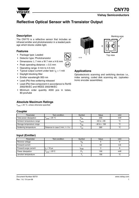
<strong>Reflective</strong> <strong>Optical</strong> <strong>Sensor</strong> <strong>with</strong> <strong>Transistor</strong> <strong>Output</strong>CNY70Vishay SemiconductorsDescriptionThe CNY70 is a reflective sensor that includes aninfrared emitter and phototransistor in a leaded packagewhich blocks visible light.EMarking areaDFeatures• Package type: Leaded• Detector type: Phototransistor• Dimensions: L 7 mm x W 7 mm x H 6 mm• Peak operating distance: < 0.5 mm e4• Operating range: 0 mm to 4.5 mm• Typical output current under test: I C = 1 mA• Daylight blocking filter• Emitter wavelength 950 nm• Lead (Pb)-free soldering released• Lead (Pb)-free component in accordance to RoHS2002/95/EC and WEEE 2002/96/EC• Minimum order quantity 4000 pcs in tubes,80 pcs/tube19158Top viewApplicationsOptoelectronic scanning and switching devices i.e.,index sensing, coded disk scanning etc. (optoelectronicencoder assemblies).Absolute Maximum RatingsT amb = 25 °C, unless otherwise specifiedCouplerParameter Test condition Symbol Value UnitTotal power dissipation T amb ≤ 25 °C P tot 200 mWAmbient temperature range T amb - 40 to + 85 °CStorage temperature range T stg - 40 to + 100 °CSoldering temperature Distance to case 2 mm, t ≤ 5 s T sd 260 °CInput (Emitter)Parameter Test condition Symbol Value UnitReverse voltage V R 5 VForward current I F 50 mAForward surge current t p ≤ 10 µs I FSM 3 APower dissipation T amb ≤ 25°C P V 100 mWJunction temperature T j 100 °CDocument Number 83751Rev. 1.6, 13-Jun-06www.vishay.com1
CNY70Vishay Semiconductors<strong>Output</strong> (Detector)Parameter Test condition Symbol Value UnitCollector emitter voltage V CEO 32 VEmitter collector voltage V ECO 7 VCollector current I C 50 mAPower dissipation T amb ≤ 25 °C P V 100 mWJunction temperature T j 100 °CElectrical CharacteristicsT amb = 25 °C, unless otherwise specifiedCouplerParameter Test condition Symbol Min Typ. Max UnitCollector currentV CE = 5 V, I F = 20 mA,1)I C0.3 1.0 mAd = 0.3 mm (figure 1)Cross talk current V CE = 5 V, I F = 20 mA (figure 1) 2)I CX600 nACollector emitter saturationvoltageI F = 20 mA, I C = 0.1 mA,d = 0.3 mm (figure 1)V CEsat1) 0.3 V1) Measured <strong>with</strong> the ‘Kodak neutral test card", white side <strong>with</strong> 90 % diffuse reflectance2) Measured <strong>with</strong>out reflecting mediumInput (Emitter)Parameter Test condition Symbol Min Typ. Max UnitForward voltage I F = 50 mA V F 1.25 1.6 V<strong>Output</strong> (Detector)Parameter Test condition Symbol Min Typ. Max UnitCollector emitter voltage I C = 1 mA V CEO 32 VEmitter collector voltage I E = 100 µA V ECO 5 VCollector dark current V CE = 20 V, I f = 0, E = 0 I CEO 200 nAwww.vishay.com2Document Number 83751Rev. 1.6, 13-Jun-06
CNY70Vishay SemiconductorsReflecting medium(Kodak neutral test card)300dEmitter~ ~~~ ~~DetectorP - Power Dissipation (mW)200100Coupled devicePhototransistorIR-diodeA C C EFigure 1. Pulse diagram95 10808095 110710 25 50 75 100T amb - Ambient Temperature (°C)Figure 2. Power Dissipation Limit vs. Ambient TemperatureTypical CharacteristicsT amb = 25 °C unless otherwise specifiedI F - Forward Current (mA)1000100101Collector Current (mA)I –C1010.10.01Kodak neutral card(white side)d= 0.3 mmV CE =5V0.10 0.2 0.4 0.6 0.8 1.0 1.2 1.4 1.6 1.8 2.096 11862 V F - Forward Voltage (V)Figure 3. Forward Current vs. Forward Voltage0.0010.1 1 1095 11065I F - Forward Current (mA)100Figure 5. Collector Current vs. Forward CurrentCTR rel - Relative Current Transfer Ratio1.51.41.31.21.11.00.90.80.70.696 11913V = 5 VCEIF= 20 mAd = 0.3 mm0.5- 30 - 20 - 10 0 10 20 30 40 50 60 70 80T amb - Ambient Temperature (°C)Collector Current (mA)I –C1010.10.0195 11066Kodak neutral card(white side)d= 0.3 mm0.0010.1 1 10I F =5 0m A20 mA10 mA5m A2m A1m AV CE - Collector Emitter Voltage (V)100Figure 4. Relative Current Transfer Ratio vs.Ambient TemperatureDocument Number 83751Rev. 1.6, 13-Jun-06Figure 6. Collector Current vs. Collector Emitter Voltagewww.vishay.com3
CNY70Vishay SemiconductorsCT R – Current Transfer Ratio (%)100101Kodak neutral card(white side)d= 0.3 mmV CE =5V0.10.1 1 10 10096 11914 I F – Forward Current (mA)Figure 7. Current Transfer Ratio vs. Forward CurrentCollector Current (mA)I –C1010.10.0010 2 4 6 895 11069V CE =5VI F =2 0m Ad– Distance (mm)Figure 9. Collector Current vs. Distanced10CT R – Current Transfer Ratio (%)1012 mAI F = 50 mA20 mA10 mA5 mA1 mAKodak neutral card(white side)d= 0.3 mm0.10.1 1 10 10096 12001 V CE – Collector Emitter Voltage (V)Figure 8. Current Transfer Ratio vs. Collector Emitter VoltageI e rel – Relative Radiant IntensityI c rel – Relative Collector Current95 110631.00.90.80.70.60° 10° 20°0.4 0.2 0 0.2 0.4Figure 10. Relative Radiant Intensity/Collector Current vs.Angular Displacement0.630°40°50°60°70°80°Relative Collector CurrentI Crel –1.00.90.80.70.60.50.40.30.20.1d=5m m4m m3m m2m m1m m0V CE =5 VI F =2 0m A1.5E D0.00 1 2 3 4 5 6 7 8 9 10 1196 11915s– Displacement (mm)EDdss05m m10 mm05m m10 mmFigure 11. Relative Collector Current vs. Displacementwww.vishay.com4Document Number 83751Rev. 1.6, 13-Jun-06
CNY70Vishay SemiconductorsPackage DimensionsDocument Number 83751Rev. 1.6, 13-Jun-06www.vishay.com5
CNY70Vishay SemiconductorsOzone Depleting Substances Policy StatementIt is the policy of Vishay Semiconductor GmbH to1. Meet all present and future national and international statutory requirements.2. Regularly and continuously improve the performance of our products, processes, distribution and operatingsystems <strong>with</strong> respect to their impact on the health and safety of our employees and the public, as well astheir impact on the environment.It is particular concern to control or eliminate releases of those substances into the atmosphere which areknown as ozone depleting substances (ODSs).The Montreal Protocol (1987) and its London Amendments (1990) intend to severely restrict the use of ODSsand forbid their use <strong>with</strong>in the next ten years. Various national and international initiatives are pressing for anearlier ban on these substances.Vishay Semiconductor GmbH has been able to use its policy of continuous improvements to eliminate the useof ODSs listed in the following documents.1. Annex A, B and list of transitional substances of the Montreal Protocol and the London Amendmentsrespectively2. Class I and II ozone depleting substances in the Clean Air Act Amendments of 1990 by the EnvironmentalProtection Agency (EPA) in the USA3. Council Decision 88/540/EEC and 91/690/EEC Annex A, B and C (transitional substances) respectively.Vishay Semiconductor GmbH can certify that our semiconductors are not manufactured <strong>with</strong> ozone depletingsubstances and do not contain such substances.We reserve the right to make changes to improve technical designand may do so <strong>with</strong>out further notice.Parameters can vary in different applications. All operating parameters must be validated for eachcustomer application by the customer. Should the buyer use Vishay Semiconductors products for anyunintended or unauthorized application, the buyer shall indemnify Vishay Semiconductors against allclaims, costs, damages, and expenses, arising out of, directly or indirectly, any claim of personaldamage, injury or death associated <strong>with</strong> such unintended or unauthorized use.Vishay Semiconductor GmbH, P.O.B. 3535, D-74025 Heilbronn, Germanywww.vishay.com6Document Number 83751Rev. 1.6, 13-Jun-06
NoticeLegal Disclaimer NoticeVishaySpecifications of the products displayed herein are subject to change <strong>with</strong>out notice. Vishay Intertechnology, Inc.,or anyone on its behalf, assumes no responsibility or liability for any errors or inaccuracies.Information contained herein is intended to provide a product description only. No license, express or implied, byestoppel or otherwise, to any intellectual property rights is granted by this document. Except as provided in Vishay'sterms and conditions of sale for such products, Vishay assumes no liability whatsoever, and disclaims any expressor implied warranty, relating to sale and/or use of Vishay products including liability or warranties relating to fitnessfor a particular purpose, merchantability, or infringement of any patent, copyright, or other intellectual property right.The products shown herein are not designed for use in medical, life-saving, or life-sustaining applications.Customers using or selling these products for use in such applications do so at their own risk and agree to fullyindemnify Vishay for any damages resulting from such improper use or sale.Document Number: 91000www.vishay.comRevision: 08-Apr-05 1