Polyimide as a Plastic Substrate for the Flexible Organic ...
Polyimide as a Plastic Substrate for the Flexible Organic ...
Polyimide as a Plastic Substrate for the Flexible Organic ...

You also want an ePaper? Increase the reach of your titles
YUMPU automatically turns print PDFs into web optimized ePapers that Google loves.
<strong>Polyimide</strong> <strong>as</strong> a Pl<strong>as</strong>tic <strong>Substrate</strong> <strong>for</strong> <strong>the</strong> <strong>Flexible</strong> <strong>Organic</strong> Electroluminescent DeviceJin-Woo Park, Youngkyoo Kim 1 , Hyuntaek Lim 2 , Cheol Min Bae, Il Kim, Shinji Ando 3 , andChang-Sik Ha*Department of Polymer Science and Engineering, Pusan National University, Busan 609 -735,Korea.1 EXSS Group, Department of Physics, The Blackett Laboratory, Imperial College London,Prince Consort Road, London SW7 2BW, UK2Device Team, NESS Display Co., Ltd., Yongin P.O.BOX 25, Kyoung Gi-Do, 449-860, Korea3 Department of <strong>Organic</strong> and Polymer Materials, Tokyo Institute of Technology, Ookayama,Meguro-Ku, Tokyo 152-8552, JapanABSTRACTIn this work, transparent flexible substrates b<strong>as</strong>ed on polyimides(PI) with indium tin oxide(ITO) thin films <strong>for</strong> organic electroluminescent devices have been prepared. 2,2’-bis-(3,4-dicarboxyphenyl) hexafluoropropanedianhydride (6FDA) and 2,2’-bis-(trifluoromethyl)-4,4’-diaminobiphenyl (TFDB) PI films were used <strong>for</strong> transparent flexible substrates. ITO thin filmswere prepared at two substrate deposition temperatures of 25˚C and 150˚C with a typical radiofrequency(r.f.) planar magnetron sputtering system. The sheet resistance and <strong>the</strong> opticaltransmission properties of <strong>the</strong> fluorinated PI substrate were comparable with those <strong>for</strong> <strong>the</strong> slidegl<strong>as</strong>s substrate. The substrate properties are better when <strong>the</strong> deposition temperature is higher.SiO 2 coating onto <strong>the</strong> fluorinated PI substrate by sol-gel reaction w<strong>as</strong> also attempted to improve<strong>the</strong> optical transmission of <strong>the</strong> ITO/PI substrate. It w<strong>as</strong> found that <strong>the</strong> coating of SiO 2 affected on<strong>the</strong> morphology of <strong>the</strong> PI substrates.INTRODUCTIONIn recent years, interests of transparent flexible pl<strong>as</strong>tic substrates with a transparentconducting oxide (TCO) layer such <strong>as</strong> ITO have been incre<strong>as</strong>ed in <strong>the</strong> fields of portable devices,roll-up displays, or con<strong>for</strong>mable displays. So far, <strong>the</strong> use of <strong>the</strong> flexible substrates <strong>for</strong> organicelectroluminescent devices (OELDs) h<strong>as</strong> been restricted mainly to <strong>the</strong> polyester films due to<strong>the</strong>ir excellent transparent property. However, <strong>the</strong> pl<strong>as</strong>tic substrates till now can be severelydamaged at high temperature during deposition process, mainly due to <strong>the</strong>ir intrinsic low <strong>the</strong>rmaland mechanical properties compared with o<strong>the</strong>r inorganic or metal substrates. Consequently,reduced electrical resistivity and long-term stability of <strong>the</strong> ITO surface cannot be achieved andmaintained, which is directly related to <strong>the</strong> per<strong>for</strong>mance of applied devices. In this sense, whollyaromatic polyimides (PI’s) are one of <strong>the</strong> best candidates <strong>for</strong> <strong>the</strong> substrate because of <strong>the</strong>irexcellent <strong>the</strong>rmal stability and good mechanical, optical, electrical, chemical properties [1].However, most aromatic PI’s are highly colored polymers with colors ranging from yellow tobrown, <strong>as</strong> well <strong>as</strong> poor processability and low solubility. Structural modification of PI’s,<strong>the</strong>re<strong>for</strong>e, h<strong>as</strong> been attempted including <strong>the</strong> incorporation of flexible bridging units [2], bulkysubstituent groups [3], and aliphatic moieties [4] into <strong>the</strong> PI backbone.In this work, colorless fluorinated polyimide substrate w<strong>as</strong> prepared with ITO thin films.On <strong>the</strong> o<strong>the</strong>r hand, some inorganic materials, such <strong>as</strong> SiO 2 were recently introduced to OELDs to
alance <strong>the</strong> number of holes and electrons injected to <strong>the</strong> emitter layer to achieve highrecombination efficiencies. In this work, <strong>the</strong>re<strong>for</strong>e, <strong>the</strong> effect of <strong>the</strong> SiO 2 buffer layer on <strong>the</strong>morphology of <strong>the</strong> colorless polyimide substrate w<strong>as</strong> also investigated. The SiO 2 buffer layerw<strong>as</strong> inserted between <strong>the</strong> polyimide substrate and ITO layers by sol-gel reaction.EXPERIMENTAL DETAILSFluorine-containing aromatic PI w<strong>as</strong> derived from 2,2’-bis-(3,4-dicarboxyphenyl)hexafluoropropane dianhydride (6FDA) and 2,2’-bis(trifluoromethyl)-4,4’-diaminobiphenyl(TFDB) [5]. The 6FDA-TFDB polyamic acid(PAA) precursor solution of dimethylacetamidewith 15 wt.% concentration w<strong>as</strong> coated onto a clean dry gl<strong>as</strong>s substrate by <strong>the</strong> solution c<strong>as</strong>tingmethod and dried at room temperature under reduced pressure. The spin-coated films were softbakedat 80˚C <strong>for</strong> 1 hour in a drying oven and dried at 150 ˚C <strong>for</strong> 1 day in a vacuum dry oven.The <strong>the</strong>rmal imidization w<strong>as</strong> per<strong>for</strong>med under nitrogen atmosphere. The thickness of <strong>the</strong>fluorinated PI substrate w<strong>as</strong> 250µm. ITO thin films were deposited onto <strong>the</strong> PI pl<strong>as</strong>tic substratesat 25˚C and 150˚C using a typical r.f. (13.56 MHz) planar magnetron sputtering system (abackground pressure; 10 -7 Torr, back filled with argon to 2.6 mTorr; 100 W, 10 min). Thecomposition of <strong>the</strong> ITO target w<strong>as</strong> 10 wt.% SnO 2 and 90 wt.% In 2 O 3 , and <strong>the</strong> distance of <strong>the</strong>target to <strong>the</strong> PI substrate w<strong>as</strong> fixed at 60 mm. There were no post-deposition annealingtreatments of ITO thin films.For silica coating on <strong>the</strong> fluorinated PI substrate, proper amounts of tetraethoxy silane(TEOS) and colloidal silica (solid contents 30wt%, water dispersion) were slowly poured into 4-necked fl<strong>as</strong>k. On adding 0.5wt% of HCl slowly with stirring, <strong>the</strong> solution w<strong>as</strong> controlled at pH4.7 and stirred <strong>for</strong> 24 hours at 30˚C <strong>for</strong> enough hydrolysis reaction. Then, to this solution excessamounts of water and ethanol were added, followed by heating at 40˚C under reduced pressurewith stirring. To make coating agents, isobutyl alcohol and ethylene glycol mono ethyl e<strong>the</strong>rwere added <strong>as</strong> diluents solvents with 0.2 wt% of a curing catalyst, tetramethyl ammonium<strong>for</strong>mate. The coating solution of 40 wt% solid content w<strong>as</strong> spin coated onto 6FDA-TFDB PIfilms at 2000 rpm <strong>for</strong> 2 min. The surface morphology and root-mean-square (RMS) roughness of<strong>the</strong>se films were me<strong>as</strong>ured at 2×2 µm 2 scan are<strong>as</strong> by atomic <strong>for</strong>ce microscopy (AFM; NanoscopeIIIa (Digital Instruments Co.)). The optical transmission spectra were me<strong>as</strong>ured with an UVvisible-nearIR spectrophotometer (CARY 5E, Varian Co.). The sheet resistance of <strong>the</strong> films w<strong>as</strong>me<strong>as</strong>ured using <strong>the</strong> four-point probe method.DISCUSSIONThe fluorinated PI derived from 2,2’-bis-(3,4-dicarboxyphenyl) hexafluoropropanedianhydride (6FDA) and 2,2’-bis(trifluoromethyl)-4,4’-diaminobiphenyl (TFDB) h<strong>as</strong> high gl<strong>as</strong>stransition and decomposition temperature, low water absorption, good transmission and lowoptical loss. The electrical sheet resistance, optical transmission, grain size and structuralorientation significantly depended on <strong>the</strong> substrate temperatures [6].The sheet resistance of <strong>the</strong> ITO film deposited at 150˚C w<strong>as</strong> much higher than that
prepared at <strong>the</strong> substrate deposition temperature of room temperature. It can be considered thatinterfacial properties between <strong>the</strong> organic polymer substrate and <strong>the</strong> metal oxide film, such <strong>as</strong>contacts, adhesions, morphologies, and interactions may be efficiently activated and improvedwith <strong>the</strong> incre<strong>as</strong>e of <strong>the</strong> substrate temperature.It is noteworthy that <strong>the</strong> sheet resistance of <strong>the</strong> ITO film deposited onto <strong>the</strong> fluorinated PIsubstrate at 150˚C is about 26.7 Ω/sq., which is higher than that of <strong>the</strong> commercial high-qualitygl<strong>as</strong>s substrate (9. 28 Ω/sq.) but much lower than that of a gl<strong>as</strong>s substrate reported in aliterature( 62.0 Ω/sq.) [7]. Most of all, <strong>the</strong> sheet resistance value w<strong>as</strong> much lower than <strong>the</strong> ITOfilms coated onto o<strong>the</strong>r polymer substrates which have been reported in <strong>the</strong> previous literatures[6,8,9].Using <strong>the</strong> dependence of <strong>the</strong> sheet resistance on <strong>the</strong> grain size, it w<strong>as</strong> considered that <strong>the</strong>predominant scattering mechanism limiting <strong>the</strong> mobility is <strong>the</strong> grain boundary scatteringmechanism <strong>for</strong> <strong>the</strong> ITO films deposited onto <strong>the</strong> PI substrates[6]. The values of <strong>the</strong> figure ofmerit in table 1 show <strong>the</strong> potential abilities of <strong>the</strong> PI substrate <strong>as</strong> transparent flexible substrateswith transparent conductive oxide thin films <strong>for</strong> optical and electrical applications, especially,flexible display devices. It w<strong>as</strong> found that <strong>the</strong> electrical sheet resistance w<strong>as</strong> slightly proportionalto <strong>the</strong> surface roughness of <strong>the</strong> ITO films[6]. Table 1 also shows <strong>the</strong> better sheet resistance valueof <strong>the</strong> fluorinated PI in comparison to that of <strong>the</strong> alicyclic PI when <strong>the</strong> deposition temperature is150 °C, which h<strong>as</strong> been syn<strong>the</strong>sized from bicyclo[2.2.2]-oct-7-ene-2,3,5,6-tetracarboxylicdianhydride (BCOEDA) and 4,4'-oxydianiline (ODA) [10, 11].The optical transmission of <strong>the</strong> ITO/PI film in <strong>the</strong> visible light range w<strong>as</strong> higher <strong>as</strong> <strong>the</strong>substrate temperature w<strong>as</strong> higher. Table 1 shows <strong>the</strong> comparison of <strong>the</strong> optical transmission <strong>as</strong>well <strong>as</strong> <strong>the</strong> sheet resistance of <strong>the</strong> fluorinated polyimide substrate with those of our previousalicyclic PI substrate[4,10]. The optical transmission of <strong>the</strong> fluorinated polyimide (at <strong>the</strong>deposition temperature of 150˚C) w<strong>as</strong> about 76% at <strong>the</strong> wavelength of 550 nm, which w<strong>as</strong> higherthat that of <strong>the</strong> alicyclic PI substrate (63 %). Table 1 indicates, however, that <strong>the</strong> opticaltransmission of <strong>the</strong> fluorinated PI substrate <strong>as</strong> well <strong>as</strong> <strong>the</strong> alicyclic PI substrate is still lower thanthat of <strong>the</strong> gl<strong>as</strong>s substrate regardless of whe<strong>the</strong>r it is commercial or home-made. Thus, <strong>the</strong>improvement of <strong>the</strong> optical transmission is needed.Table 1. The sheet resistance of <strong>the</strong> ITO films deposited onto <strong>the</strong> fluorinated and <strong>the</strong> aliphaticcyclic polyimide substrates prepared at two different deposition temperatures.<strong>Substrate</strong>Growth Avg.Sheet Figure of meritTemp. Transmission*resistance F TC(400-700 nm)(℃)(Ω/sq.) (×10 -3 Ω -1 ) [12](%)Alicyclic PI [10] 2515060.163.069.234.68.618.2Fluorinated PI[6] 2515066.276.0126.526.75.2328.5Gl<strong>as</strong>s [6](commercial ITO)- 83.4 9.28 89.8Gl<strong>as</strong>s [7](sputtering)130 85.0 62.0 14.0* F TC = T (optical transmission) / R s (electrical sheet resistance)
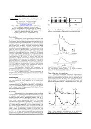
Recently some inorganic materials, such <strong>as</strong> SiO 2 were introduced to OELDs to balance<strong>the</strong> number of holes and electrons injected to <strong>the</strong> emitter layer to achieve high recombinationefficiencies [13]. An attempt to obtain better electric conduction properties h<strong>as</strong> been made byinsertion of a SiO 2 buffer layer between <strong>the</strong> poly (ethylene terephthalate) (PET) and ITO layers(ITO/SiO 2 /PET) [14]. Incre<strong>as</strong>ing <strong>the</strong> adhesion between <strong>the</strong> PET and ITO by <strong>the</strong> inserted SiO 2anchor layer also enhanced scribbling durability when <strong>the</strong> ITO / PET substrate w<strong>as</strong> used <strong>for</strong> aresistive touch panel [14, 15]. In this work, <strong>the</strong>re<strong>for</strong>e, we also attempted to insert SiO 2 bufferlayer in between ITO and <strong>the</strong> colorless fluorinated PI substrate in order to enhance <strong>the</strong> opticaltransmission per<strong>for</strong>mance of <strong>the</strong> flexible transparent substrate prepared.To apply a thin SiO 2 layer onto <strong>the</strong> fluorinated PI substrate, nano-sized colloidal silicaw<strong>as</strong> mixed with TEOS, which w<strong>as</strong> hydrolyzed and condensed with <strong>the</strong> silanol groups on <strong>the</strong>surface of silica. Coating films are made from <strong>the</strong>se solutions on <strong>the</strong> fluorinated PI substrate.(a)(b)Figure 1. The AFM 2-D images (2 µm×2µm scan area) of <strong>the</strong> 6FDA- TFDB polyimide film (a)and polyimide film coated with SiO 2 (b).Roughness: 1.777nmRoughness: 1.081nm(a)(b)Figure 2. The AFM 3-D images (2 µm×2µm scan area) and root-mean- square (RMS) roughnessof <strong>the</strong> 6FDA-TFDB polyimide film (a) and polyimide film coated with SiO 2 (b).
Figure 1 shows <strong>the</strong> AFM 2-D images of <strong>the</strong> fluorinated PI film and <strong>the</strong> SiO 2 coated PI film.The bare PI substrate shows a typical surface morphology of uni<strong>for</strong>m flat amorphous polymerswithout any crystalline or agglomerate <strong>for</strong>mation. Pinholes of PI’s are, however, observed hereand <strong>the</strong>re during film preparation. It is noteworthy that <strong>the</strong> surface morphology of PI coated withSiO 2 is much better than uncoated PI because pinholes of PI are occupied by SiO 2 . Figure 2shows <strong>the</strong> AFM 3-D images and root-mean-square (RMS) surface roughness of <strong>the</strong> fluorinatedPI film and <strong>the</strong> PI film coated with SiO 2 . It is important to note that <strong>the</strong> surface roughness of <strong>the</strong>PI coated with SiO 2 film decre<strong>as</strong>ed because of <strong>the</strong> smoo<strong>the</strong>r surface in comparison to <strong>the</strong> PI filmwithout SiO 2 layer.Smooth surface with unevenness of less than about 0.7nm w<strong>as</strong> obtained <strong>for</strong> <strong>the</strong> PI filmcoated with SiO 2 . This low surface roughness may affect on <strong>the</strong> sheet resistance <strong>for</strong> sputteredITO film. It w<strong>as</strong> reported that better electric conductivity properties were observed by insertionof a SiO 2 anchor layer between <strong>the</strong> PI substrate and ITO layers [15]. Noda and Tanimurareported that <strong>the</strong> presence of SiO 2 anchor layer may induce a vitreous state of <strong>the</strong> PI surface,which h<strong>as</strong> an affinity with ITO [16].The optical transmission of <strong>the</strong> SiO 2 coated 6FDA-TFDB PI film reached to about 89%when optimized, while <strong>the</strong> average optical transmission of <strong>the</strong> 6FDA-TFDB PI substrate withoutSiO 2 w<strong>as</strong> lower in <strong>the</strong> visible light range, <strong>as</strong> shown in table 1. It w<strong>as</strong> mentioned that <strong>the</strong>syn<strong>the</strong>sized aromatic PI substrate is optically colorless, transparent, and inactive, overcoming amajor disadvantage of typical aromatic PI’s <strong>as</strong> well <strong>as</strong> extending application fields [4,6]. Theseresults are attributed to <strong>the</strong> minimization of <strong>the</strong> <strong>for</strong>mation of <strong>the</strong> intra- and/or intermolecularcharge transfer complex (CTC) in <strong>the</strong> PI molecules. It is important to note that <strong>the</strong> opticaltransmission of <strong>the</strong> PI film coated with SiO 2 incre<strong>as</strong>ed slightly (over 2%) compared withuncoated 6FDA-TFDB PI film. The results suggest that very smooth surface of coating agentscomposed of TEOS and colloidal silica reduced light scattering on <strong>the</strong> film surface.Future studies will focus on <strong>the</strong> deposition of ITO onto <strong>the</strong> SiO 2 coated 6FDA-TFDB PIsubstrate will be described elsewhere. It may be expected that <strong>the</strong> PI substrate coated with SiO 2thin film can be a suitable candidate <strong>for</strong> flexible display devices with high transparency and goodelectrical properties.CONCLUSIONSIn summary, <strong>the</strong> per<strong>for</strong>mance of <strong>the</strong> ITO film with <strong>the</strong> 6FDA-TFDB PI substrate such <strong>as</strong>optical transmission and sheet resistance w<strong>as</strong> sufficiently comparable with that of <strong>the</strong> gl<strong>as</strong>ssubstrateITO film, and <strong>the</strong> PI substrate might be an excellent candidate <strong>for</strong> transparent flexiblesubstrates in <strong>the</strong> flat panel display or o<strong>the</strong>r electronic applications. ITO thin films were preparedat two substrate deposition temperatures of 25˚C and 150˚C with a typical radio-frequency planarmagnetron sputtering system. The sheet resistance and <strong>the</strong> optical transmission properties of <strong>the</strong>fluorinated PI substrate were comparable with those <strong>for</strong> <strong>the</strong> slide gl<strong>as</strong>s substrate. The substrateproperties are better when <strong>the</strong> deposition temperature is high. The effect of <strong>the</strong> SiO 2 coating on<strong>the</strong> morphology of colorless fluorinated polyimide substrates <strong>for</strong> OELDs w<strong>as</strong> also investigated.To coat a thin SiO 2 layer, suspensions containing colloidal silica and TEOS were applied on <strong>the</strong>PI substrate by sol-gel reaction. Optical transmission of <strong>the</strong> SiO 2 coated 6FDA-TFDB PI filmw<strong>as</strong> significantly incre<strong>as</strong>ed compared with <strong>the</strong> uncoated PI film, due to <strong>the</strong> decre<strong>as</strong>e of surface
oughness.ACKNOWLEDGEMENTSThe work w<strong>as</strong> supported by <strong>the</strong> National Research Laboratory Program, <strong>the</strong> Center <strong>for</strong>Integrated Molecular Systems, POSTECH, Korea and <strong>the</strong> Brain Korea 21 Project.REFERENCES1. Y. Kim, J. Keum, J.G. Kim, H. Lim, and C.S. Ha,. Adv. Mater. Opt. Electron., 10, 273 (2000).2. G. C. E<strong>as</strong>tmond, J. Paprotny and R. S. Irwin, Macromolecules, 29, 1382 (1996).3. W. G. Kim and A. S. Hay, Macromolecules, 26, 5275 (1993).4. H. Lim, C. Bae, J. Park, W.J. Cho, and C.S. Ha, Synth. Metal. 137, 1017 (2003).5. S. Matsuda, S. Ando and T. Sawada, Electron. Lett. 37, 706 (2001).6. H. Lim, W.J. Cho, C.S. Ha, S. Ando, Y.K. Kim, C.H. Park, and K. Lee, Adv. Mater. 14, 1275(2002).7. W. F. Wu, B. S. Chiou and S. T. Hsieh, Semicond. Sci. Technol. 9, 1242 (1994).8. S. Yamamoto, T. Yamanaka and Z. Ueda, J. Vac. Sci. Technol. A5, 1957 (1987).9. H. Kim, C. M. Gilmore, A. Pique, J. S. Horwitz, H. Mattoussi, H. Murata, Z. H. Kafafi, andD. B. Chrisey, J. Appl. Phys. 86, 6451 (1999).10. H. Lim, Ph.D.dissertation, Pusan National University, Korea (2002).11. S. Itamura, M. Yamada, S. Tamura, T. Matsumoto, and T. Kurosaki, Macromolecules, 26,3490 (1993).12. D. B. Fr<strong>as</strong>er and H. D. Cook, J. Electrochem. Soc. 119, 1368 (1972).13. Z. B. Deng, X. M. Ding, S. T. Lee, and W. A. Gambling, Appl. Phys. Lett. 74, 2227 (1999).14. D. Goto and H. Anayama, Japanese Patent, HI-132005 (1989).15. S. Yamamoto, Z. Ueda and K. S<strong>as</strong>a, Nitto Tech Rep (in Japanese). (1986).16. K. Noda and K. Tanimura, Electron. and Commun. Jpn. 84, 39 (2001).