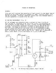
TL594 Precision Switchmode Pulse Width Modulation Control Circuit
TL594 Precision Switchmode Pulse Width Modulation Control Circuit
TL594 Precision Switchmode Pulse Width Modulation Control Circuit
- No tags were found...

You also want an ePaper? Increase the reach of your titles
YUMPU automatically turns print PDFs into web optimized ePapers that Google loves.
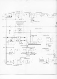
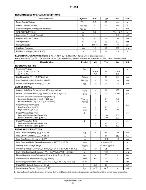
<strong>TL594</strong>RECOMMENDED OPERATING CONDITIONSCharacteristics Symbol Min Typ Max UnitPower Supply Voltage V CC 7.0 15 40 VCollector Output Voltage V C1 , V C2 – 30 40 VCollector Output Current (Each transistor) I C1 , I C2 – – 200 mAAmplified Input Voltage V in 0.3 – V CC – 2.0 VCurrent Into Feedback Terminal l fb – – 0.3 mAReference Output Current l ref – – 10 mATiming Resistor R T 1.8 30 500 kΩTiming Capacitor C T 0.0047 0.001 10 µFOscillator Frequency f osc 1.0 40 200 kHzPWM Input Voltage (Pins 3, 4, 13) – 0.3 – 5.3 VELECTRICAL CHARACTERISTICS (V CC = 15 V, C T = 0.01 µF, R T = 12 kΩ, unless otherwise noted.)For typical values T A = 25°C, for min/max values T A is the operating ambient temperature range that applies, unless otherwise noted.Characteristics Symbol Min Typ Max UnitVREFERENCE SECTIONReference VoltageV(I O = 1.0 mA, T A = 25°C)(I O = 1.0 mA)ref4.9254.95.0–5.0755.1Line Regulation (V CC = 7.0 V to 40 V) Reg line – 2.0 25 mVLoad Regulation (I O = 1.0 mA to 10 mA) Reg load – 2.0 15 mVShort <strong>Circuit</strong> Output Current (V ref = 0 V) I SC 15 40 75 mAOUTPUT SECTIONCollector Off–State Current (V CC = 40 V, V CE = 40 V) I C(off) – 2.0 100 µAEmitter Off–State Current (V CC = 40 V, V C = 40 V, V E = 0 V) I E(off) – – –100 µACollector–Emitter Saturation Voltage (Note 2.)Common–Emitter (V E = 0 V, I C = 200 mA)Emitter–Follower (V C = 15 V, I E = –200 mA)V SAT(C)V SAT(E)––1.11.51.32.5VOutput <strong>Control</strong> Pin CurrentLow State (V OC ≤ 0.4 V)High State (V OC = V ref )Output Voltage Rise TimeCommon–Emitter (See Figure 13)Emitter–Follower (See Figure 14)Output Voltage Fall TimeCommon–Emitter (See Figure 13)Emitter–Follower (See Figure 14)I OCL –I OCH –t r––t f––ERROR AMPLIFIER SECTIONInput Offset Voltage (V O (Pin 3) = 2.5 V) V IO – 2.0 10 mVInput Offset Current (V O (Pin 3) = 2.5 V) I IO – 5.0 250 nAInput Bias Current (V O (Pin 3) = 2.5 V) I IB – –0.1 –1.0 µAInput Common Mode Voltage Range (V CC = 40 V, T A = 25°C) V ICR 0 to V CC –2.0 VInverting Input Voltage Range V IR(INV) –0.3 to V CC –2.0 VOpen Loop Voltage Gain (∆V O = 3.0 V, V O = 0.5 V to 3.5 V, R L = 2.0 kΩ) A VOL 70 95 – dBUnity–Gain Crossover Frequency (V O = 0.5 V to 3.5 V, R L = 2.0 kΩ) f C – 700 – kHzPhase Margin at Unity–Gain (V O = 0.5 V to 3.5 V, R L = 2.0 kΩ) φm – 65 – deg.Common Mode Rejection Ratio (V CC = 40 V) CMRR 65 90 – dBPower Supply Rejection Ratio (∆V CC = 33 V, V O = 2.5 V, R L = 2.0 kΩ) PSRR – 100 – dBOutput Sink Current (V O (Pin 3) = 0.7 V) I O – 0.3 0.7 – mAOutput Source Current (V O (Pin 3) = 3.5 V) I O + –2.0 –4.0 – mA2. Low duty cycle pulse techniques are used during test to maintain junction temperature as close to ambient temperature as possible.0.12.01001004040–20200200100100µAnsnshttp://onsemi.com2