TL594 Precision Switchmode Pulse Width Modulation Control Circuit
TL594 Precision Switchmode Pulse Width Modulation Control Circuit
TL594 Precision Switchmode Pulse Width Modulation Control Circuit
- No tags were found...

You also want an ePaper? Increase the reach of your titles
YUMPU automatically turns print PDFs into web optimized ePapers that Google loves.
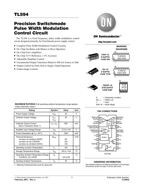
The <strong>TL594</strong> is a fixed frequency, pulse width modulation controlcircuit designed primarily for <strong>Switchmode</strong> power supply control.http://onsemi.com• Complete <strong>Pulse</strong> <strong>Width</strong> <strong>Modulation</strong> <strong>Control</strong> <strong>Circuit</strong>ry• On–Chip Oscillator with Master or Slave Operation• On–Chip Error Amplifiers• On–Chip 5.0 V Reference, 1.5% Accuracy• Adjustable Deadtime <strong>Control</strong>• Uncommitted Output Transistors Rated to 500 mA Source or Sink• Output <strong>Control</strong> for Push–Pull or Single–Ended Operation• Undervoltage Lockout161611PDIP–16N SUFFIXCASE 648SO–16D SUFFIXCASE 751BMARKINGDIAGRAMS161161<strong>TL594</strong>CNAWLYWW<strong>TL594</strong>CDAWLYWW16161TSSOP–16DTB SUFFIXCASE 948F1<strong>TL594</strong>DTBALYWMAXIMUM RATINGS (Full operating ambient temperature range applies,unless otherwise noted.)Rating Symbol Value UnitPower Supply Voltage V CC 42 VCollector Output Voltage V C1 ,V C242 VCollector Output Current(Each Transistor) (Note 1.)I C1 , I C2 500 mAAmplifier Input Voltage Range V IR –0.3 to +42 VPower Dissipation @ T A ≤ 45°C P D 1000 mWThermal ResistanceJunction–to–Ambient (PDIP)Junction–to–Air (TSSOP)Junction–to–Ambient (SOIC)R θJA80140135°C/WOperating Junction Temperature T J 125 °CStorage Temperature Range T stg –55 to +125 °COperating Ambient Temperature Range<strong>TL594</strong>CD, CN, CDTBT A–25 to 85Derating Ambient Temperature T A 45 °C1. Maximum thermal limits must be observed.°C A = Assembly LocationWL, L = Wafer LotY = YearWW, W = Work WeekPIN CONNECTIONS ≈ ORDERING INFORMATIONSee detailed ordering and shipping information in the packagedimensions section on page 10 of this data sheet. © Semiconductor Components Industries, LLC, 2001February, 2001 – Rev. 21 Publication Order Number:<strong>TL594</strong>/D
<strong>TL594</strong>RECOMMENDED OPERATING CONDITIONSCharacteristics Symbol Min Typ Max UnitPower Supply Voltage V CC 7.0 15 40 VCollector Output Voltage V C1 , V C2 – 30 40 VCollector Output Current (Each transistor) I C1 , I C2 – – 200 mAAmplified Input Voltage V in 0.3 – V CC – 2.0 VCurrent Into Feedback Terminal l fb – – 0.3 mAReference Output Current l ref – – 10 mATiming Resistor R T 1.8 30 500 kΩTiming Capacitor C T 0.0047 0.001 10 µFOscillator Frequency f osc 1.0 40 200 kHzPWM Input Voltage (Pins 3, 4, 13) – 0.3 – 5.3 VELECTRICAL CHARACTERISTICS (V CC = 15 V, C T = 0.01 µF, R T = 12 kΩ, unless otherwise noted.)For typical values T A = 25°C, for min/max values T A is the operating ambient temperature range that applies, unless otherwise noted.Characteristics Symbol Min Typ Max UnitVREFERENCE SECTIONReference VoltageV(I O = 1.0 mA, T A = 25°C)(I O = 1.0 mA)ref4.9254.95.0–5.0755.1Line Regulation (V CC = 7.0 V to 40 V) Reg line – 2.0 25 mVLoad Regulation (I O = 1.0 mA to 10 mA) Reg load – 2.0 15 mVShort <strong>Circuit</strong> Output Current (V ref = 0 V) I SC 15 40 75 mAOUTPUT SECTIONCollector Off–State Current (V CC = 40 V, V CE = 40 V) I C(off) – 2.0 100 µAEmitter Off–State Current (V CC = 40 V, V C = 40 V, V E = 0 V) I E(off) – – –100 µACollector–Emitter Saturation Voltage (Note 2.)Common–Emitter (V E = 0 V, I C = 200 mA)Emitter–Follower (V C = 15 V, I E = –200 mA)V SAT(C)V SAT(E)––1.11.51.32.5VOutput <strong>Control</strong> Pin CurrentLow State (V OC ≤ 0.4 V)High State (V OC = V ref )Output Voltage Rise TimeCommon–Emitter (See Figure 13)Emitter–Follower (See Figure 14)Output Voltage Fall TimeCommon–Emitter (See Figure 13)Emitter–Follower (See Figure 14)I OCL –I OCH –t r––t f––ERROR AMPLIFIER SECTIONInput Offset Voltage (V O (Pin 3) = 2.5 V) V IO – 2.0 10 mVInput Offset Current (V O (Pin 3) = 2.5 V) I IO – 5.0 250 nAInput Bias Current (V O (Pin 3) = 2.5 V) I IB – –0.1 –1.0 µAInput Common Mode Voltage Range (V CC = 40 V, T A = 25°C) V ICR 0 to V CC –2.0 VInverting Input Voltage Range V IR(INV) –0.3 to V CC –2.0 VOpen Loop Voltage Gain (∆V O = 3.0 V, V O = 0.5 V to 3.5 V, R L = 2.0 kΩ) A VOL 70 95 – dBUnity–Gain Crossover Frequency (V O = 0.5 V to 3.5 V, R L = 2.0 kΩ) f C – 700 – kHzPhase Margin at Unity–Gain (V O = 0.5 V to 3.5 V, R L = 2.0 kΩ) φm – 65 – deg.Common Mode Rejection Ratio (V CC = 40 V) CMRR 65 90 – dBPower Supply Rejection Ratio (∆V CC = 33 V, V O = 2.5 V, R L = 2.0 kΩ) PSRR – 100 – dBOutput Sink Current (V O (Pin 3) = 0.7 V) I O – 0.3 0.7 – mAOutput Source Current (V O (Pin 3) = 3.5 V) I O + –2.0 –4.0 – mA2. Low duty cycle pulse techniques are used during test to maintain junction temperature as close to ambient temperature as possible.0.12.01001004040–20200200100100µAnsnshttp://onsemi.com2
<strong>TL594</strong>ELECTRICAL CHARACTERISTICS (V CC = 15 V, C T = 0.01 µF, R T = 12 kΩ, unless otherwise noted.)For typical values T A = 25°C, for min/max values T A is the operating ambient temperature range that applies, unless otherwise noted.Characteristics Symbol Min Typ Max UnitPWM COMPARATOR SECTION (Test <strong>Circuit</strong> Figure 11)Input Threshold Voltage (Zero Duty Cycle) V TH – 3.6 4.5 VInput Sink Current (V Pin 3 = 0.7 V) I I– 0.3 0.7 – mADEADTIME CONTROL SECTION (Test <strong>Circuit</strong> Figure 11)Input Bias Current (Pin 4) (V Pin 4 = 0 V to 5.25 V) I IB (DT) – –2.0 –10 µAMaximum Duty Cycle, Each Output, Push–Pull Mode(V Pin 4 = 0 V, C T = 0.01 µF, R T = 12 kΩ)(V Pin 4 = 0 V, C T = 0.001 µF, R T = 30 kΩ)Input Threshold Voltage (Pin 4)(Zero Duty Cycle)(Maximum Duty Cycle)OSCILLATOR SECTIONFrequency(C T = 0.001 µF, R T = 30 kΩ)(C T = 0.01 µF, R T = 12 kΩ, T A = 25°C)(C T = 0.01 µF, R T = 12 kΩ, T A = T low to T high )DC max45–V TH–0f osc–9.29.0Standard Deviation of Frequency* (C T = 0.001 µF, R T = 30 kΩ) σf osc – 1.5 – %Frequency Change with Voltage (V CC = 7.0 V to 40 V, T A = 25°C) ∆f osc (∆V) – 0.2 1.0 %Frequency Change with Temperature(∆T A = T low to T high , C T = 0.01 µF, R T = 12 kΩ)48452.8–4010–50–3.3––10.812%VkHz∆f osc (∆T) – 4.0 – %UNDERVOLTAGE LOCKOUT SECTIONTurn–On Threshold (V CC Increasing, I ref = 1.0 mA)V thT A = 25°C4.0T A = T low to T high 3.55.2–6.06.5VHysteresis<strong>TL594</strong>C,I<strong>TL594</strong>MV H10050150150300300mVTOTAL DEVICEStandby Supply Current (Pin 6 at V ref , All other inputs and outputsopen)(V CC = 15 V)(V CC = 40 V)I CC––Average Supply Current (V Pin 4 = 2.0 V, C T = 0.01 µF, R T = 12 kΩ,V CC = 15 V, See Figure 11) – 11 –8.08.01518mAmA*Standard deviation is a measure of the statistical distribution about the mean as derived from the formula, σNΣ (X n – X) 2n = 1N – 1http://onsemi.com3
<strong>TL594</strong> ≈ ≈ This device contains 46 active transistors.Figure 1. Representative Block Diagram Figure 2. Timing Diagramhttp://onsemi.com4
<strong>TL594</strong>APPLICATIONS INFORMATIONDescriptionThe <strong>TL594</strong> is a fixed–frequency pulse widthmodulation control circuit, incorporating the primarybuilding blocks required for the control of a switchingpower supply. (See Figure 1.) An internal–linear sawtoothoscillator is frequency– programmable by two externalcomponents, R T and C T . The approximate oscillatorfrequency is determined by:f osc ≈ 1.1R T • C TFor more information refer to Figure 3.Output pulse width modulation is accomplished bycomparison of the positive sawtooth waveform acrosscapacitor C T to either of two control signals. The NOR gates,which drive output transistors Q1 and Q2, are enabled onlywhen the flip–flop clock–input line is in its low state. Thishappens only during that portion of time when the sawtoothvoltage is greater than the control signals. Therefore, anincrease in control–signal amplitude causes a correspondinglinear decrease of output pulse width. (Refer to the TimingDiagram shown in Figure 2.)The control signals are external inputs that can be fed intothe deadtime control, the error amplifier inputs, or thefeedback input. The deadtime control comparator has aneffective 120 mV input offset which limits the minimumoutput deadtime to approximately the first 4% of thesawtooth–cycle time. This would result in a maximum dutycycle on a given output of 96% with the output controlgrounded, and 48% with it connected to the reference line.Additional deadtime may be imposed on the output bysetting the deadtime–control input to a fixed voltage,ranging between 0 V to 3.3 V.The pulse width modulator comparator provides a meansfor the error amplifiers to adjust the output pulse width fromthe maximum percent on–time, established by the deadtimecontrol input, down to zero, as the voltage at the feedbackpin varies from 0.5 V to 3.5 V. Both error amplifiers have acommon–mode input range from –0.3 V to (V CC – 2 V), andmay be used to sense power–supply output voltage andcurrent. The error–amplifier outputs are active high and areORed together at the noninverting input of the pulse–widthmodulator comparator. With this configuration, theamplifier that demands minimum output on time, dominatescontrol of the loop.Input/Output<strong>Control</strong>sFunctional TableOutput Functionf outf osc=Grounded Single–ended PWM @ Q1 and Q2 1.0@ V ref Push–pull Operation 0.5When capacitor C T is discharged, a positive pulse isgenerated on the output of the deadtime comparator, whichclocks the pulse–steering flip–flop and inhibits the outputtransistors, Q1 and Q2. With the output–control connectedto the reference line, the pulse–steering flip–flop directs themodulated pulses to each of the two output transistorsalternately for push–pull operation. The output frequency isequal to half that of the oscillator. Output drive can also betaken from Q1 or Q2, when single–ended operation with amaximum on–time of less than 50% is required. This isdesirable when the output transformer has a ringbackwinding with a catch diode used for snubbing. When higheroutput–drive currents are required for single–endedoperation, Q1 and Q2 may be connected in parallel, and theoutput–mode pin must be tied to ground to disable theflip–flop. The output frequency will now be equal to that ofthe oscillator.The <strong>TL594</strong> has an internal 5.0 V reference capable ofsourcing up to 10 mA of load current for external biascircuits. The reference has an internal accuracy of ±1.5%with a typical thermal drift of less than 50 mV over anoperating temperature range of 0° to 70°C. µµ µ ΩFigure 3. Oscillator Frequency versusTiming Resistance ∆ ΩFigure 4. Open Loop Voltage Gain andPhase versus Frequency φφhttp://onsemi.com5
<strong>TL594</strong> µµ µ Ω µ Ω Figure 5. Percent Deadtime versusOscillator FrequencyFigure 6. Percent Duty Cycle versusDeadtime <strong>Control</strong> Voltage Figure 7. Emitter–Follower ConfigurationOutput Saturation Voltage versusEmitter CurrentFigure 8. Common–Emitter ConfigurationOutput Saturation Voltage versusCollector Current Figure 9. Standby Supply Currentversus Supply Voltage Figure 10. Undervoltage Lockout Thresholdsversus Reference Load Currenthttp://onsemi.com6
<strong>TL594</strong> Figure 11. Error–Amplifier CharacteristicsFigure 12. Deadtime and Feedback <strong>Control</strong> <strong>Circuit</strong> Figure 13. Common–Emitter ConfigurationTest <strong>Circuit</strong> and WaveformFigure 14. Emitter–Follower ConfigurationTest <strong>Circuit</strong> and Waveformhttp://onsemi.com7
<strong>TL594</strong> Figure 15. Error–Amplifier Sensing Techniques ≈ Figure 16. Deadtime <strong>Control</strong> <strong>Circuit</strong>Figure 17. Soft–Start <strong>Circuit</strong>≤ ≤ ≤ ≤ Figure 18. Output Connections for Single–Ended and Push–Pull Configurationshttp://onsemi.com8
<strong>TL594</strong> Figure 19. Slaving Two or More <strong>Control</strong> <strong>Circuit</strong>sFigure 20. Operation with V in > 40 V UsingExternal Zener µTest Conditions ResultsLine Regulation V in = 10 V to 40 V 14 mV 0.28%Load Regulation V in = 28 V, I O = 1.0 mA to 1.0 A 3.0 mV 0.06%Output Ripple V in = 28 V, I O = 1.0 A 65 mVpp P.A.R.D.Short <strong>Circuit</strong> Current V in = 28 V, R L = 0.1 Ω 1.6 AEfficiency V in = 28 V, I O = 1.0 A 71%Figure 21. <strong>Pulse</strong> <strong>Width</strong> Modulated Push–Pull Converterhttp://onsemi.com9
<strong>TL594</strong> <strong>TL594</strong> Test Conditions ResultsLine Regulation V in = 8.0 V to 40 V 3.0 mV 0.01%Load Regulation V in = 12.6 V, I O = 0.2 mA to 200 mA 5.0 mV 0.02%Output Ripple V in = 12.6 V, I O = 200 mA 40 mVpp P.A.R.D.Short <strong>Circuit</strong> Current V in = 12.6 V, R L = 0.1 Ω 250 mAEfficiency V in = 12.6 V, I O = 200 mA 72%Figure 22. <strong>Pulse</strong> <strong>Width</strong> Modulated Step–Down ConverterDeviceORDERING INFORMATIONOperatingTemperature Range Package Shipping<strong>TL594</strong>CD –25 to 85°C SOIC–16 48 Units/Rail<strong>TL594</strong>CDR2 –25 to 85°C SOIC–16 2400 Tape & Reel<strong>TL594</strong>CN –25 to 85°C PDIP–16 25 Units/Rail<strong>TL594</strong>CDTB –25 to 85°C TSSOP–16 96 Units/Rail<strong>TL594</strong>CDTBR2 –25 to 85°C TSSOP–16 2500 Tape & Reelhttp://onsemi.com10
<strong>TL594</strong>PACKAGE DIMENSIONSPDIP–16N SUFFIXCASE 648–08ISSUE R16–A–9B1 8 HGFSCKD 16 PL –T– JLM °° °°SOIC–16D SUFFIXCASE 751B–05ISSUE J–T –161 8G–A–9–B–K P 8 PLCM R X 45°JF °° °°http://onsemi.com11
<strong>TL594</strong>PACKAGE DIMENSIONS –T– LPIN 1IDENT.D2X L/2C16X K REF 16 91 8A–V–GTSSOP–16DTB SUFFIXCASE 948F–01ISSUE OB–U– NJJ1KK1ÇÇÇSECTION N–NÉÉÉ ÇÇÇÉÉÉM N F DETAIL E –W– H DETAIL E ON Semiconductor and are trademarks of Semiconductor Components Industries, LLC (SCILLC). SCILLC reserves the right to make changeswithout further notice to any products herein. SCILLC makes no warranty, representation or guarantee regarding the suitability of its products for any particularpurpose, nor does SCILLC assume any liability arising out of the application or use of any product or circuit, and specifically disclaims any and all liability,including without limitation special, consequential or incidental damages. “Typical” parameters which may be provided in SCILLC data sheets and/orspecifications can and do vary in different applications and actual performance may vary over time. All operating parameters, including “Typicals” must bevalidated for each customer application by customer’s technical experts. SCILLC does not convey any license under its patent rights nor the rights of others.SCILLC products are not designed, intended, or authorized for use as components in systems intended for surgical implant into the body, or other applicationsintended to support or sustain life, or for any other application in which the failure of the SCILLC product could create a situation where personal injury ordeath may occur. Should Buyer purchase or use SCILLC products for any such unintended or unauthorized application, Buyer shall indemnify and holdSCILLC and its officers, employees, subsidiaries, affiliates, and distributors harmless against all claims, costs, damages, and expenses, and reasonableattorney fees arising out of, directly or indirectly, any claim of personal injury or death associated with such unintended or unauthorized use, even if such claimalleges that SCILLC was negligent regarding the design or manufacture of the part. SCILLC is an Equal Opportunity/Affirmative Action Employer.PUBLICATION ORDERING INFORMATIONNORTH AMERICA Literature Fulfillment:Literature Distribution Center for ON SemiconductorP.O. Box 5163, Denver, Colorado 80217 USAPhone: 303–675–2175 or 800–344–3860 Toll Free USA/CanadaFax: 303–675–2176 or 800–344–3867 Toll Free USA/CanadaEmail: ONlit@hibbertco.comFax Response Line: 303–675–2167 or 800–344–3810 Toll Free USA/CanadaN. American Technical Support: 800–282–9855 Toll Free USA/CanadaEUROPE: LDC for ON Semiconductor – European SupportGerman Phone: (+1) 303–308–7140 (Mon–Fri 2:30pm to 7:00pm CET)Email: ONlit–german@hibbertco.comFrench Phone: (+1) 303–308–7141 (Mon–Fri 2:00pm to 7:00pm CET)Email: ONlit–french@hibbertco.comEnglish Phone: (+1) 303–308–7142 (Mon–Fri 12:00pm to 5:00pm GMT)Email: ONlit@hibbertco.comEUROPEAN TOLL–FREE ACCESS*: 00–800–4422–3781*Available from Germany, France, Italy, UK, IrelandCENTRAL/SOUTH AMERICA:Spanish Phone: 303–308–7143 (Mon–Fri 8:00am to 5:00pm MST)Email: ONlit–spanish@hibbertco.comToll–Free from Mexico: Dial 01–800–288–2872 for Access –then Dial 866–297–9322ASIA/PACIFIC: LDC for ON Semiconductor – Asia SupportPhone: 303–675–2121 (Tue–Fri 9:00am to 1:00pm, Hong Kong Time)Toll Free from Hong Kong & Singapore:001–800–4422–3781Email: ONlit–asia@hibbertco.comJAPAN: ON Semiconductor, Japan Customer Focus Center4–32–1 Nishi–Gotanda, Shinagawa–ku, Tokyo, Japan 141–0031Phone: 81–3–5740–2700Email: r14525@onsemi.comON Semiconductor Website: http://onsemi.comFor additional information, please contact your localSales Representative.http://onsemi.com12<strong>TL594</strong>/D