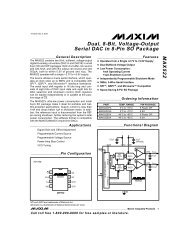
MAX9157 Quad Bus LVDS Transceiver - Maxim
MAX9157 Quad Bus LVDS Transceiver - Maxim
MAX9157 Quad Bus LVDS Transceiver - Maxim

Create successful ePaper yourself
Turn your PDF publications into a flip-book with our unique Google optimized e-Paper software.
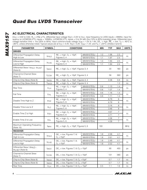
<strong>Quad</strong> <strong>Bus</strong> <strong>LVDS</strong> <strong>Transceiver</strong><strong>MAX9157</strong>AC ELECTRICAL CHARACTERISTICS(V CC = 3.0V to 3.6V, R L = 27Ω ±1%, differential input voltage |V ID | = 0.2V to V CC , input frequency to <strong>LVDS</strong> inputs = 85MHz, input frequencyto LVCMOS/LVTTL inputs = 100MHz, LVCMOS/LVTTL inputs = 0 to 3V with 2ns (10% to 90%) transition times. Differential inputvoltage transition time = 1ns (20% to 80%). Input common-mode voltage V CM = 1.2V to 1.8V, DE_ = high, RE_ = low, T A = -40°C to+85°C, unless otherwise noted. Typical values are at V CC = 3.3V, |V ID | = 0.2V, V CM = 1.2V, and T A = +25°C.) (Notes 3 and 5)DRIVERPARAMETER SYMBOL CONDITIONS MIN TYP MAX UNITSDifferential Propagation DelayHigh to LowDifferential Propagation DelayLow to Hight PHLDt PLHDRE_ = high, C L = 10pF, <strong>MAX9157</strong>EGJ 1.2 1.96 2.5Figures 3, 4 <strong>MAX9157</strong>EHJ 1.1 1.87 2.4RE_ = high, C L = 10pF, <strong>MAX9157</strong>EGJ 1.2 1.94 2.5Figures 3, 4 <strong>MAX9157</strong>EHJ 1.1 1.84 2.4nsnsDifferential Skew | t PHLD - t PLHD |(Note 6)Channel-to-Channel Skew(Note 7)t SKD1 RE_ = high, C L = 10pF, Figures 3, 4 33 160 pst CCSK RE_ = high, C L = 10pF, Figures 3, 4 58 300 psChip-to-Chip Skew (Note 8) t SKD2 RE_ = high, C L = 10pF, Figures 3, 4 0.38 0.8 nsChip-to-Chip Skew (Note 9) T SKD3 RE_ = high, C L = 10pF, Figures 3, 4 1.3 nsRE_ = high, C <strong>MAX9157</strong>EGJ 0.6 1.13 1.4Rise Time t L = 10pF,TLHFigures 3, 4 <strong>MAX9157</strong>EHJ 0.6 1.07 1.4RE_ = high, C <strong>MAX9157</strong>EGJ 0.6 1.16 1.4Fall Time t L = 10pF,THLFigures 3, 4 <strong>MAX9157</strong>EHJ 0.6 1.11 1.4RE_ = high, C <strong>MAX9157</strong>EGJ 6.79 8Disable Time High to Z t L = 10pF,PHZFigures 5, 6 <strong>MAX9157</strong>EHJ 6.79 8RE_ = high, C <strong>MAX9157</strong>EGJ 3.16 8Disable Time Low to Z t L = 10pF,PLZFigures 5, 6 <strong>MAX9157</strong>EHJ 3.48 8RE_ = high, C <strong>MAX9157</strong>EGJ 4.67 7Enable Time Z to High t L = 10pF,PZHFigures 5, 6 <strong>MAX9157</strong>EHJ 4.71 7RE_ = high, C <strong>MAX9157</strong>EGJ 4.36 7Enable Time Z to Low t L = 10pF,PZLFigures 5, 6 <strong>MAX9157</strong>EHJ 4.39 7nsnsnsnsnsns<strong>Maxim</strong>um Operating Frequency(Note 10)f MAX RE_ = high, C L = 10pF, Figures 5, 6 100 MHzRECEIVERDifferential Propagation DelayHigh to LowDifferential Propagation DelayLow to HighDE_ = low, Figures 7, 8; <strong>MAX9157</strong>EGJ 1.8 2.58 4.1t PHLDC L =15pF <strong>MAX9157</strong>EHJ 1.8 2.61 4.1DE_ = low, Figures 7, 8; <strong>MAX9157</strong>EGJ 1.8 2.49 4.1t PLHDC L =15pF <strong>MAX9157</strong>EHJ 1.8 2.52 4.1nsnsDifferential Skew | tPHLD -tPLHD | (Note 6)Channel-to-Channel Skew(Note 7)t SKD1 DE_ = low, Figures 7, 8; C L = 15pF 90 450 pst CCSK DE_ = low, Figures 7, 8; C L = 15pF 131 580 psChip-to-Chip Skew (Note 8) t SKD2 DE_ = low, Figures 7, 8; C L =15pF 0.7 1.7 nsChip-to-Chip Skew (Note 9) t SKD3 DE_ = low, Figures 7, 8; C L =15pF 0.7 1.7 nsRise Time t TLH DE_ = low, Figures 7, 8; C L = 15pF 0.5 1.1 1.6 ns4 _______________________________________________________________________________________