LA4598 - Datasheet Catalog
LA4598 - Datasheet Catalog
LA4598 - Datasheet Catalog

You also want an ePaper? Increase the reach of your titles
YUMPU automatically turns print PDFs into web optimized ePapers that Google loves.
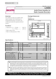
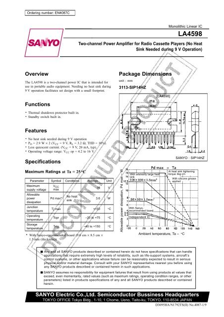
Ordering number: EN4087CMonolithic Linear IC<strong>LA4598</strong>Two-channel Power Amplifier for Radio Cassette Players (No HeatSink Needed during 9VOperation)OverviewThe <strong>LA4598</strong> is a two-channel power IC that is intended foruse in portable audio equipment. Needing no heat sink during9 V operation facilitates set design with a small footprint.Functions. Thermal shutdown protector built in.. Standby switch built in.Package Dimensionsunit : mm3113-SIP14HZ[<strong>LA4598</strong>]FeaturesNo heat sink needed during 9 V operationPO = 2.9 W × 2(V CC =9V,R L = 3.2 Ω, THD = 10%).Less quiescent current. (VCC = 9 V, 20 mA, typ).. Operating voltage range: VCC op = 4.2 to 16 V.SpecificationsMaximum Ratings atTa=25°CParameter Symbol Conditions Ratings UnitMaximumsupply voltageAllowablepowerdissipationJunctiontemperatureOperatingtemperatureStoragetemperatureV CCmaxPd max*No heatsink18 V3.6 WTj max +150 °CTopr –20 to +75 °CTstg –40 to +150 °C* With Sanyo-recommended board (9.0 cm × 8.5 cm ×1.5 mm (thickness))Allowable power dissipation, Pd max – WWith arbitrarily large heatsinkWith SanyorecommendedboardIndependent ICSANYO : SIP14HZAl heat sink tighteningtorque 4kg . cmWith silicone greaseappliedAmbient temperature, Ta – °CAny and all SANYO products described or contained herein do not have specifications that can handleapplications that require extremely high levels of reliability, such as life-support systems, aircraft’scontrol systems, or other applications whose failure can be reasonably expected to result in seriousphysical and/or material damage. Consult with your SANYO representative nearest you before usingany SANYO products described or contained herein in such applications.SANYO assumes no responsibility for equipment failures that result from using products at values thatexceed, even momentarily, rated values (such as maximum ratings, operating condition ranges, or otherparameters) listed in products specifications of any and all SANYO products described or containedherein.SANYO Electric Co.,Ltd. Semiconductor Bussiness HeadquartersTOKYO OFFICE Tokyo Bldg., 1-10, 1 Chome, Ueno, Taito-ku, TOKYO, 110-8534 JAPAND3095HA/N1792TS(II) No.4087-1/9
<strong>LA4598</strong>Operating Conditions atTa=25°CParameter Symbol Conditions Ratings UnitRecommended supply voltage V CC 9 VRecommended load resistance R L 3.2 ΩOperating voltage range V CC op 4.2 to 16.0 VOperating Characteristics atTa=25°C, V CC =9V,f=1kHz, Rg = 600 Ω, R L = 3.2 ΩParameter Symbol Conditions min typ max unitQuiescent current I CCO 10 20 40 mAVoltage gain VG 47 49 51 dBOutput powerP O 1 THD = 10% 2.2 2.9 WP O 2 THD = 10%, R L =4Ω 2.3 WTotal harmonic distortion THD V O = 2 V 0.3 1.0 %Input resistance ri 20 30 kΩOutput noise voltageV NO1 Rg = 0, B.P.F = 20 Hz to 20 kHz 0.4 1.0 mVV NO2 Rg=10kΩ, B.P.F = 20 Hz to 20 kHz 0.6 2.0 mVRipple rejection ratio Rr Rg = 0, fr = 100 Hz, V CC r = 150 mV 40 50 dBChannel separation CH Sep Rg = 10 kΩ, V O =0dB 45 55 dBStandby current Isd 10 µABlock Diagramch1 Inputch1 NFInputamplifierPredriveamplifierPoweramplifierch1 BSch1 outputPre GNDPower GNDD.CBias circuitThermal shutdownprotectorV CCStandby switchStandbych2 Inputch2 NFInputamplifierPredriveamplifierPoweramplifierch2 outputch2 BSSample Print PatternCopper-foiled side 85 × 90 mm 2Unit (resistance: Ω, capacitance: F)No.4087-2/9
<strong>LA4598</strong>Sample Application CircuitTo large signal GNDMylar capacitorUnit (resistance:Ω, capacitance:F)Mylar capacitorC + R can be added to the negative side of the output capacitor.However, this is true only for a Sanyo-recommended board; for a set board, artwork must also beconsidered.Description of External ComponentsC 1 ,C 8 : Bootstrap capacitorsThese capacitors affect low-region output; if the capacitor value is reduced, the low-region output decreases. Therefore,47 µF or more is desirable.C 2 ,C 6 : Output capacitorsIf the capacitor value is reduced, low-region roll-off frequency f L and low-region Po worsen.C 3 ,C 7 : Oscillation blocking capacitorsMylar capacitor, which is excellent in temperature characteristics and frequency characteristics is used.C 4 :C 5 :Power supply capacitorThe capacitor values depends on the power supply line loads (motor, and the like.) and transformer ripple component.1000 µF to 2200 µF is recommended.Standby capacitorPop noise reduction capacitorC 9 ,C 11 : Feedback capacitorsIn addition to affecting low-region roll-off frequency f L , if the capacitor value is increased, the start-up time is extended.C 10 :Decoupling capacitorThis capacitor absorbs power supply ripples; 220 µF is recommended.R 1 ,R 2 : Oscillation blocking resistorsThe resistor value may be varied 3.3 Ω to 1.0 Ω.No.4087-3/9
<strong>LA4598</strong>Total harmonic distortion, THD – %Current drain, I CC – APd when V CC =12 VPd when 9 VPower dissipation, Pd – WFrequency, f – HzOutput power, P O – WCurrent drain, I CC – APower dissipation, Pd – WCurrent drain, I CC – APower dissipation, Pd – WOutput power, P O – WOutput power, P O – WmAQuiescent current, I CCO – mAOutput power, P O – WSupply voltage, V CC – VSupply voltage, V CC – VNo.4087-4/9
<strong>LA4598</strong>Channel separation – dBCH2 to CH1leakCH1 to CH2leakTotal harmonic distortion, THD – %Frequency, f – HzSupply voltage, V CC – VResponse – dBTotal harmonic distortion, THD – %Frequency, f – HzOutput power, P O – WOutput ripple noise voltage, V NOR – mVOutput noise voltage, V NO – mVDIN Audio with20 Hz to 20 kHz BPFSupply voltage, V CC – VSupply voltage, V CC – VNo.4087-5/9
<strong>LA4598</strong>Output ripple noise voltage, V NOR – mVOutput ripple noise voltage, V NOR – mVΩRipple frequency, f R – HzPower supply ripple, V R – mVBTL Sample Application CircuitTo large signal GNDUnit (resistance:Ω, capacitance:F)Mylar capacitorC + R can be added to the negative side of the output capacitor.However, this is true only for a Sanyo-recommended board; for a set board, artwork must also be considered.No.4087-6/9
<strong>LA4598</strong>Output power, P O – WCurrent drain, I CC – APower dissipation, Pd – WCurrent drain, I CC – APower dissipation, Pd – WOutput power, P O – WOutput power, P O – WTotal harmonic distortion, THD – %Supply voltage, V CC – VOutput power, P O – WResponse – dBFrequency, f – HzNo.4087-7/9
<strong>LA4598</strong>Features and Usage Notes1. VG can be lowered by adding an R NF ’ to the NF pins (pins 5 and 11).Calculated as follows:VG = 20log R f /(R NF +R NF ’)The IC contains R f =20kΩ, R NF =62Ω.However, the following must be noted:a) If R NF ’ is added, the ripple bypass effect due to the NF capacitor will worsen, resulting in a worsening of ripplerejection.b) Oscillation stability requires, use at 40 dB or less to be avoided.2. Pin 9 is intended for standby. It is used in conjunction with power supply pin 4. However, it should be noted that whenpower supply pin 9 and pin 4 are used for separate systems, the output power is affected by the pin 9 supply voltage.3. It is recommendable to use no input capacitor. However when rubbing noise generated by the volume control is offencive tothe ear, an input capacitor must be inserted.4. Extreme caution must be exercised when the IC is used in the vincity of the maximum ratings, since even a slight variationin conditions may cause the maximum ratings to be exceeded, thereby leading to breakdown.5. When making the board, refer to the sample printed circuit pattern. No feedback loop must be formed between input andoutput. Thick and short wiring is required so that no common resistance exists between the preamplifier GND and poweramplifier GND.6. Addition of components as shown below enables use without introducing an increased distortion at V CC of up toapproximately 4.5 V. A capacitor of 470 µF is inserted against pop noise.Proper Cares in Mounting a Radiator Fin1. The tightening torque should be in a range from 4 to 6 kg.cm.2. The spacing between the screw holes of the radiator fin must match the spacing between the screw holes of the IC. With caseoutline dimensions L and R referred to, the screws must be tightened with the distance between them as close to each otheras possible.3. The screws to be used must have a head equivalent to the one of truss machine screw or binder machine screw defined byJIS. Washers must also be used to protect the IC case.4. No foreign matter such as cutting particles should exist between heat sink and radiator fin. When applying grease on thejunction surface, it must be applied uniformly on the whole surface.5. IC lead pins should be soldered to the printed circuit board after the radiator fin is mounted on the IC.No.4087-8/9
<strong>LA4598</strong>Specifications of any and all SANYO products described or contained herein stipulate the performance,characteristics, and functions of the described products in the independent state, and are not guaranteesof the performance, characteristics, and functions of the described products as mounted in the customer’sproducts or equipment. To verify symptoms and states that cannot be evaluated in an independent device,the customer should always evaluate and test devices mounted in the customer’s products or equipment.SANYO Electric Co., Ltd. strives to supply high-quality high-reliability products. However, any and allsemiconductor products fail with some probability. It is possible that these probabilistic failures couldgive rise to accidents or events that could endanger human lives, that could give rise to smoke or fire,or that could cause damage to other property. When designing equipment, adopt safety measures sothat these kinds of accidents or events cannot occur. Such measures include but are not limited to protectivecircuits and error prevention circuits for safe design, redundant design, and structural design.In the event that any or all SANYO products(including technical data,services) described orcontained herein are controlled under any of applicable local export control laws and regulations,such products must not be exported without obtaining the export license from the authoritiesconcerned in accordance with the above law.No part of this publication may be reproduced or transmitted in any form or by any means, electronic ormechanical, including photocopying and recording, or any information storage or retrieval system,or otherwise, without the prior written permission of SANYO Electric Co., Ltd.Any and all information described or contained herein are subject to change without notice due toproduct/technology improvement, etc. When designing equipment, refer to the “Delivery Specification”for the SANYO product that you intend to use.Information (including circuit diagrams and circuit parameters) herein is for example only ; it is notguaranteed for volume production. SANYO believes information herein is accurate and reliable, butno guarantees are made or implied regarding its use or any infringements of intellectual property rightsor other rights of third parties.This catalog provides information as of December, 1995. Specifications and information herein are subject tochange without notice.PS No.4087-9/9
This datasheet has been download from:www.datasheetcatalog.com<strong>Datasheet</strong>s for electronics components.