TDA7386 - Tehnari.ru
TDA7386 - Tehnari.ru
TDA7386 - Tehnari.ru

You also want an ePaper? Increase the reach of your titles
YUMPU automatically turns print PDFs into web optimized ePapers that Google loves.
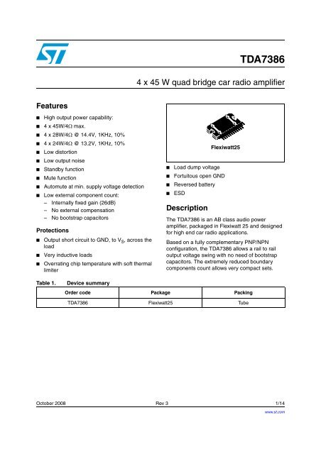
<strong>TDA7386</strong>4 x 45 W quad bridge car radio amplifierFeatures■■High output power capability:4 x 45W/4Ω max.■ 4 x 28W/4Ω @ 14.4V, 1KHz, 10%■ 4 x 24W/4Ω @ 13.2V, 1KHz, 10%■■■■■■Low distortionLow output noiseStandby functionMute functionAutomute at min. supply voltage detectionLow external component count:– Internally fixed gain (26dB)– No external compensation– No bootstrap capacitorsProtections■ Output short circuit to GND, to V S , across theload■ Very inductive loads■ Overrating chip temperature with soft thermallimiter■■■■Load dump voltageFortuitous open GNDReversed batteryESDDescriptionFlexiwatt25The <strong>TDA7386</strong> is an AB class audio poweramplifier, packaged in Flexiwatt 25 and designedfor high end car radio applications.Based on a fully complementary PNP/NPNconfiguration, the <strong>TDA7386</strong> allows a rail to railoutput voltage swing with no need of bootstrapcapacitors. The extremely reduced boundarycomponents count allows very compact sets.Table 1.Device summaryOrder code Package Packing<strong>TDA7386</strong> Flexiwatt25 TubeOctober 2008 Rev 3 1/14www.st.com1
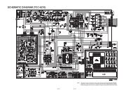
Contents<strong>TDA7386</strong>Contents1 Block and pin connection diagrams . . . . . . . . . . . . . . . . . . . . . . . . . . . . 52 Electrical specifications . . . . . . . . . . . . . . . . . . . . . . . . . . . . . . . . . . . . . . 62.1 Absolute maximum ratings . . . . . . . . . . . . . . . . . . . . . . . . . . . . . . . . . . . . . 62.2 Thermal data . . . . . . . . . . . . . . . . . . . . . . . . . . . . . . . . . . . . . . . . . . . . . . . 62.3 Electrical characteristics . . . . . . . . . . . . . . . . . . . . . . . . . . . . . . . . . . . . . . . 62.4 PCB and component layout . . . . . . . . . . . . . . . . . . . . . . . . . . . . . . . . . . . . 82.5 Electrical characteristics curves . . . . . . . . . . . . . . . . . . . . . . . . . . . . . . . . . 93 Application hints . . . . . . . . . . . . . . . . . . . . . . . . . . . . . . . . . . . . . . . . . . . 113.1 SVR . . . . . . . . . . . . . . . . . . . . . . . . . . . . . . . . . . . . . . . . . . . . . . . . . . . . . 113.2 Input stage . . . . . . . . . . . . . . . . . . . . . . . . . . . . . . . . . . . . . . . . . . . . . . . . 113.3 Standby and muting . . . . . . . . . . . . . . . . . . . . . . . . . . . . . . . . . . . . . . . . . 114 Package information . . . . . . . . . . . . . . . . . . . . . . . . . . . . . . . . . . . . . . . . 125 Revision history . . . . . . . . . . . . . . . . . . . . . . . . . . . . . . . . . . . . . . . . . . . 132/14
<strong>TDA7386</strong>List of tablesList of tablesTable 1. Device summary . . . . . . . . . . . . . . . . . . . . . . . . . . . . . . . . . . . . . . . . . . . . . . . . . . . . . . . . . . 1Table 2. Absolute maximum ratings . . . . . . . . . . . . . . . . . . . . . . . . . . . . . . . . . . . . . . . . . . . . . . . . . . 6Table 3. Thermal data. . . . . . . . . . . . . . . . . . . . . . . . . . . . . . . . . . . . . . . . . . . . . . . . . . . . . . . . . . . . . 6Table 4. Electrical characteristics . . . . . . . . . . . . . . . . . . . . . . . . . . . . . . . . . . . . . . . . . . . . . . . . . . . . 6Table 5. Document revision history . . . . . . . . . . . . . . . . . . . . . . . . . . . . . . . . . . . . . . . . . . . . . . . . . 133/14
<strong>TDA7386</strong>Block and pin connection diagrams1 Block and pin connection diagramsFigure 1.Block diagramVcc1Vcc22200µF100nFST-BYIN1IN2IN3IN4MUTE0.1µF0.1µF0.1µF0.1µFAC-GNDSVR TAB S-GND0.47µF 47µFN.C.OUT1+OUT1-PW-GNDOUT2+OUT2-PW-GNDOUT3+OUT3-PW-GNDOUT4+OUT4-PW-GNDD99AU1018AFigure 2.Pin connection (top view)1 25TABP-GND2ST-BYOUT2+P-GND1OUT1+SVRIN1IN2S-GNDIN4IN3AC-GNDOUT3+P-GND3VCCOUT4+MUTEOUT2-VCCOUT1-OUT3-OUT4-P-GND4N.C.D94AU159B5/14
Electrical specifications<strong>TDA7386</strong>2 Electrical specifications2.1 Absolute maximum ratingsTable 2.Absolute maximum ratingsSymbol Parameter Value UnitV CC Operating supply voltage 18 VV CC (DC) DC supply voltage 28 VV CC (pk) Peak supply voltage (t = 50ms) 50 VI OOutput peak current:Repetitive (Duty Cycle 10% at f = 10Hz)Non Repetitive (t = 100μs)P tot Power dissipation, (T case = 70°C) 80 WT j Junction temperature 150 °CT stg Storage temperature – 55 to 150 °C4.55.5AA2.2 Thermal dataTable 3. Thermal dataSymbol Parameter Value UnitR th j-case Thermal resistance junction to case max. 1 °C/W2.3 Electrical characteristicsTable 4.Electrical characteristicsV S = 14.4 V; f = 1 kHz; R g = 600 Ω; R L = 4 Ω; T amb = 25 °C; Refer to the test and applicationdiagram, unless otherwise specified.Symbol Parameter Test condition Min. Typ. Max. UnitI q1 Quiescent current R L = ∞ 190 350 mAV OS Output offset voltage Play Mode ±80 mVΔV OSDuring mute on/off outputoffset voltage±80 mVG v Voltage gain 25 26 27 dBΔG v Channel gain unbalance ±1 dBTHD = 10%; V S = 13.2V 22 24 WP o Output powerTHD = 0.8%; V S = 13.2V 16.5 18 WTHD = 10%; V S = 14.4V 26 28 WP o max Max.output power (1) V S = 14.4V 43 45 WTHD Distortion P o = 4W 0.04 0.15 %6/14
<strong>TDA7386</strong>Electrical specificationsTable 4.e No Output noise"A" Weighted 50 70 μVBw = 20 Hz to 20 kHz 70 100 μVSVR Supply voltage rejection f = 100 Hz; V r = 1V rms 50 75 dBf ch High cut-off frequency P o = 0.5 W 80 200 KHzR i Input impedance 70 100 KΩC TCross talkf = 1 kHz; Po = 4 W 60 70 dBf = 10 kHz; Po = 4W 60 dBI SBStandby currentV St-by = 1.5 50 μAconsumptionV St-by = 0 V 20 μAI pin4 Standby pin current V St-by = 1.5 to 3.5 V ±1 μAV SB outStandby out thresholdvoltage(Amp: on) 3.5 VV SB IN Standby in threshold voltage (Amp: off) 1.5 VA M Mute attenuation P Oref = 4W 80 90 dBV M out Mute out threshold voltage (Amp: play) 3.5 VV M in Mute in threshold voltage (Amp: mute) 1.5 VV AM inI pin22Electrical characteristics (continued)V S = 14.4 V; f = 1 kHz; R g = 600 Ω; R L = 4 Ω; T amb = 25 °C; Refer to the test and applicationdiagram, unless otherwise specified.Symbol Parameter Test condition Min. Typ. Max. UnitV S automute thresholdMuting pin current1. Saturated square wave output.(Amp: mute); Att ≥ 80dB; P Oref = 4Ω(Amp: play); Att < 0.1dB; P O = 0.5Ω 7.66.58.5V MUTE = 1.5V (Source current) 5 11 20 μAV MUTE = 3.5V -5 - 20 μAVVFigure 3.Standard test and application circuitC80.1μFC72200μFVcc1-2Vcc3-4ST-BYMUTEIN1R110KR247KC10.1μFC91μFC101μF422116 20987523OUT1OUT2IN21217C2 0.1μF18OUT3IN31519C3 0.1μF21IN41424OUT4C4 0.1μFS-GND1316 10 25 123C50.47μFSVRC647μFN.C.TAB7/14
Electrical specifications<strong>TDA7386</strong>2.4 PCB and component layoutReferred to the circuit of Figure 3.Figure 4.Components and top copper layerFigure 5.Bottom copper layer8/14
<strong>TDA7386</strong>Electrical specifications2.5 Electrical characteristics curvesFigure 6. Quiescent current vs. supply voltage Figure 7. Quiescent output voltage vs. supplyvoltageFigure 8. Output power vs. supply voltage Figure 9. Max. output power vs. supply voltageFigure 10. Distortion vs. output powerFigure 11. Distortion vs. frequency9/14
Electrical specifications<strong>TDA7386</strong>Figure 12. Supply voltage rejection vs.frequencyFigure 13. Crosstalk vs. frequencyFigure 14. Output noise vs. source resistanceFigure 15. Power dissipation and efficiency vs.output power10/14
<strong>TDA7386</strong>Application hints3 Application hintsReferred to the circuit of Figure 3.3.1 SVRBesides its contribution to the ripple rejection, the SVR capacitor governs the turn ON/OFFtime sequence and, consequently, plays an essential role in the pop optimization duringON/OFF transients.To conveniently serve both needs, ITS MINIMUM RECOMMENDED VALUE IS 10μF.3.2 Input stageThe <strong>TDA7386</strong>’s inputs are ground-compatible and can stand very high input signals (±8Vpk)without any performances degradation.If the standard value for the input capacitors (0.1μF) is adopted, the low frequency cut-offwill amount to 16 Hz.3.3 Standby and mutingStandby and muting facilities are both CMOS-compatible. If unused, a straight connection toVs of their respective pins would be admissible.Conventional/low-power transistors can be employed to drive muting and stand-by pins inabsence of t<strong>ru</strong>e CMOS ports or microprocessors. R-C cells have always to be used in orderto smooth down the transitions for preventing any audible transient noises.Since a DC current of about 10 µA normally flows out of pin 22, the maximum allowablemuting-series resistance (R 2 ) is 70 KΩ, which is sufficiently high to permit a mutingcapacitor reasonably small (about 1µF).If R 2 is higher than recommended, the involved risk will be that the voltage at pin 22 may riseto above the 1.5 V threshold voltage and the device will consequently fail to turn OFF whenthe mute line is brought down.About the stand-by, the time constant to be assigned in order to obtain a virtually pop-freetransition has to be slower than 2.5V/ms.11/14
Package information<strong>TDA7386</strong>4 Package informationIn order to meet environmental requirements, ST (also) offers these devices in ECOPACK ®packages. ECOPACK ® packages are lead-free. The category of second Level Interconnectis marked on the package and on the inner box label, in compliance with JEDEC StandardJESD97. The maximum ratings related to soldering conditions are also marked on the innerbox label.ECOPACK is an ST trademark. ECOPACK specifications are available at: www.st.com.Figure 16. Flexiwatt25 mechanical data and package dimensionsDIM.mminchMIN. TYP. MAX. MIN. TYP. MAX.A 4.45 4.50 4.65 0.175 0.177 0.183B 1.80 1.90 2.00 0.070 0.074 0.079C 1.40 0.055D 0.75 0.90 1.05 0.029 0.035 0.041E 0.37 0.39 0.42 0.014 0.015 0.016F (1) 0.57 0.022G 0.80 1.00 1.20 0.031 0.040 0.047G1 23.75 24.00 24.25 0.935 0.945 0.955H (2) 28.90 29.23 29.30 1.139 1.150 1.153H1 17.00 0.669H2 12.80 0.503H3 0.80 0.031L (2) 22.07 22.47 22.87 0.869 0.884 0.904L1 18.57 18.97 19.37 0.731 0.747 0.762L2 (2) 15.50 15.70 15.90 0.610 0.618 0.626L3 7.70 7.85 7.95 0.303 0.309 0.313L4 5 0.197L5 3.5 0.138M 3.70 4.00 4.30 0.145 0.157 0.169M1 3.60 4.00 4.40 0.142 0.157 0.173N 2.20 0.086O 2 0.079R 1.70 0.067R1 0.5 0.02R2 0.3 0.12R3 1.25 0.049R4 0.50 0.019V5˚ (T p.)V13˚ (Typ.)V220˚ (Typ.)V345˚ (Typ.)(1): dam-bar protusion not included(2): molding protusion includedOUTLINE ANDMECHANICAL DATAFlexiwatt25 (vertical)VCBV3H3HH1H2VAOR3L2L3 L4NR4V2RR2LL1V1V1R2R1DPin 1GG1FFLEX25MEL5 R1 R1EM M1703486212/14
<strong>TDA7386</strong>Revision history5 Revision historyTable 5. Document revision historyDate Revision Changes24-Nov-2001 1 Initial release.20-Dec-2007 2Document reformatted.Modified the Features on page 1.Modified the Figure 1 and 2.Updated the Table 4: Electrical characteristics.29-Oct-2008 3 Updated the Table 3: Thermal data on page 6.13/14
<strong>TDA7386</strong>Please Read Carefully:Information in this document is provided solely in connection with ST products. STMicroelectronics NV and its subsidiaries (“ST”) reserve theright to make changes, corrections, modifications or improvements, to this document, and the products and services described herein at anytime, without notice.All ST products are sold pursuant to ST’s terms and conditions of sale.Purchasers are solely responsible for the choice, selection and use of the ST products and services described herein, and ST assumes noliability whatsoever relating to the choice, selection or use of the ST products and services described herein.No license, express or implied, by estoppel or otherwise, to any intellectual property rights is granted under this document. If any part of thisdocument refers to any third party products or services it shall not be deemed a license grant by ST for the use of such third party productsor services, or any intellectual property contained therein or considered as a warranty covering the use in any manner whatsoever of suchthird party products or services or any intellectual property contained therein.UNLESS OTHERWISE SET FORTH IN ST’S TERMS AND CONDITIONS OF SALE ST DISCLAIMS ANY EXPRESS OR IMPLIEDWARRANTY WITH RESPECT TO THE USE AND/OR SALE OF ST PRODUCTS INCLUDING WITHOUT LIMITATION IMPLIEDWARRANTIES OF MERCHANTABILITY, FITNESS FOR A PARTICULAR PURPOSE (AND THEIR EQUIVALENTS UNDER THE LAWSOF ANY JURISDICTION), OR INFRINGEMENT OF ANY PATENT, COPYRIGHT OR OTHER INTELLECTUAL PROPERTY RIGHT.UNLESS EXPRESSLY APPROVED IN WRITING BY AN AUTHORIZED ST REPRESENTATIVE, ST PRODUCTS ARE NOTRECOMMENDED, AUTHORIZED OR WARRANTED FOR USE IN MILITARY, AIR CRAFT, SPACE, LIFE SAVING, OR LIFE SUSTAININGAPPLICATIONS, NOR IN PRODUCTS OR SYSTEMS WHERE FAILURE OR MALFUNCTION MAY RESULT IN PERSONAL INJURY,DEATH, OR SEVERE PROPERTY OR ENVIRONMENTAL DAMAGE. ST PRODUCTS WHICH ARE NOT SPECIFIED AS "AUTOMOTIVEGRADE" MAY ONLY BE USED IN AUTOMOTIVE APPLICATIONS AT USER’S OWN RISK.Resale of ST products with provisions different from the statements and/or technical features set forth in this document shall immediately voidany warranty granted by ST for the ST product or service described herein and shall not create or extend in any manner whatsoever, anyliability of ST.ST and the ST logo are trademarks or registered trademarks of ST in various countries.Information in this document supersedes and replaces all information previously supplied.The ST logo is a registered trademark of STMicroelectronics. All other names are the property of their respective owners.© 2008 STMicroelectronics - All rights reservedSTMicroelectronics group of companiesAustralia - Belgium - Brazil - Canada - China - Czech Republic - Finland - France - Germany - Hong Kong - India - Israel - Italy - Japan -Malaysia - Malta - Morocco - Singapore - Spain - Sweden - Switzerland - United Kingdom - United States of Americawww.st.com14/14