Novel Nano Novel Nano-Engineered Semiconductors for ... - Caltech
Novel Nano Novel Nano-Engineered Semiconductors for ... - Caltech
Novel Nano Novel Nano-Engineered Semiconductors for ... - Caltech

Create successful ePaper yourself
Turn your PDF publications into a flip-book with our unique Google optimized e-Paper software.
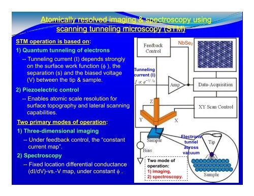
Atomically resolved imaging & spectroscopy usingscanning tunneling microscopy (STM)STM operation is based on:1) Quantum tunneling of electrons-- Tunneling current (I) depends stronglyon the surface work function ( ), theseparation (s) and the biased voltage(V) between the tip & sample.2) Piezoelectric control-- Enables atomic scale resolution <strong>for</strong>surface topography and lateral scanningcapabilities.iTwo primary modes of operation:1) Three-dimensional imaging-- Under feedback control, the “constantcurrent map”.2) Spectroscopy-- Fixed location differential conductance(dI/dV)-vs.-V map, under constant .Tunnelingcurrent (I)Two mode ofoperation:1) imaging,2) spectroscopy.NbSe 2Electronstunnelacrossvacuum