Novel Nano Novel Nano-Engineered Semiconductors for ... - Caltech
Novel Nano Novel Nano-Engineered Semiconductors for ... - Caltech
Novel Nano Novel Nano-Engineered Semiconductors for ... - Caltech

Create successful ePaper yourself
Turn your PDF publications into a flip-book with our unique Google optimized e-Paper software.
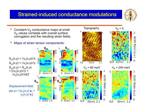
Strained-induced induced conductance modulations• Constant-V B conductance maps at smallV B values correlate with overall surfacecorrugation and the resulting strain fields.Topography V B = 0• Maps of strain tensor components:S 00V B = 80 meV V B = 240 meVS 00S xxS xx (x,y) = u x (x,y)/xS yy (x,y) = u y (x,y)/yS xy (x,y) = S xy (x,y)= [u x (x,y)/y +u y (x,y)/x]/2Displacement field:u(x,y) = [u x (x,y) e x +u y (x,y) e y ]S xyS yy