WA02Y ±5%, ±1% Convex Type General purpose chip resistors ...
WA02Y ±5%, ±1% Convex Type General purpose chip resistors ...
WA02Y ±5%, ±1% Convex Type General purpose chip resistors ...

Create successful ePaper yourself
Turn your PDF publications into a flip-book with our unique Google optimized e-Paper software.
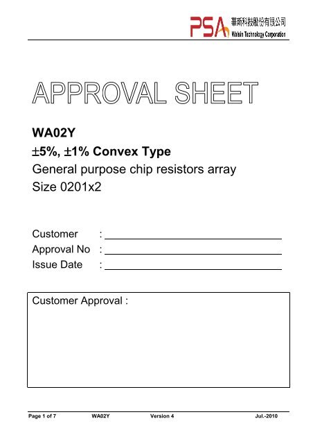
<strong>WA02Y</strong>±5%, ±1% <strong>Convex</strong> <strong>Type</strong><strong>General</strong> <strong>purpose</strong> <strong>chip</strong> <strong>resistors</strong> arraySize 0201x2Customer :Approval No :Issue Date :Customer Approval :Page 1 of 7 <strong>WA02Y</strong> Version 4 Jul.-2010
FEATURE1. Small size and light weight2. Reduced size of final equipment3. Lower surface mounted assembly costs4. Higher component and equipment reliabilityAPPLICATION• Consumer electrical equipment, PDA, Digital Cam-coder, …• EDP, Computer application• Mobile phone, Telecom• Ram moduleDESCRIPTIONThe <strong>resistors</strong> array is constructed in a high grade ceramic body (aluminum oxide). Internal metal electrodes areadded at each end and connected by a resistive paste that is applied to the top surface of the substrate. Thecomposition of the paste is adjusted to give the approximate resistance required and the value is trimmed towithin tolerance by laser cutting of this resistive layer.The resistive layer is covered with a protective coat. Finally, the two external end terminations are added. Forease of soldering the outer layer of these end terminations is a Tin (lead free) solder alloy.Fig 1. Outline of <strong>chip</strong>-R array <strong>WA02Y</strong>Page 2 of 7 <strong>WA02Y</strong> Version 4 Jul.-2010
QUICK REFERENCE DATAItemSeries No.SizeTermination constructionResistance ToleranceResistance Range<strong>General</strong> Specification<strong>WA02Y</strong>0201x2 (0603x2)<strong>Convex</strong> type±5%, ±1% (E24 series)10Ω ~ 1MΩ, Jumper (< 50mΩ)TCR (ppm/°C)Max. dissipation at T amb=70°C≤ ± 300 ppm/°C1/32 WMax. Operation Voltage (DC or RMS) 12.5VMax. overload voltageRated current for Jumper 0.5AClimatic category (IEC 60068) 55/125/56Note :1. This is the maximum voltage that may be continuously supplied to the resistor element, see “IEC publication60115-8”2. Max. Operation Voltage : So called RCWV (Rated Continuous Working Voltage) is determined byRCWV = Rated Power × Resistance Value or Max. RCWV listed above, whichever is lower.25VDimensions<strong>WA02Y</strong>L 0.80 ± 0.10WW 0.60 ± 0.10T 0.35 ± 0.10P 0.50 ± 0.10TaPTTbA 0.35 ± 0.10Ta 0.15 ± 0.10Tb 0.15 ± 0.10ALPage 3 of 7 <strong>WA02Y</strong> Version 4 Jul.-2010
MarkingNo marking for <strong>WA02Y</strong> <strong>chip</strong> <strong>resistors</strong> arrayFUNCTIONAL DESCRIPTIONProduct characterizationStandard values of nominal resistance are taken from the E24 series for <strong>resistors</strong> with a tolerance of ±5%,±1%. The values of the E24 series are in accordance with “IEC publication 60063”DeratingThe power that the resistor can dissipate depends on the operating temperature; see Fig.2Figure 2. Maximum dissipation in percentage of rated powerAs a function of the ambient temperatureCONSTRUCTIONMOUNTINGR1=R2Due to their rectangular shapes and small tolerances, Surface Mountable Resistors are suitable for handling byautomatic placement systems.Chip placement can be on ceramic substrates and printed-circuit boards (PCBs).Electrical connection to the circuit is by individual soldering condition.The end terminations guarantee a reliable contact.Page 4 of 7 <strong>WA02Y</strong> Version 4 Jul.-2010
SOLDERING CONDITIONThe robust construction of <strong>chip</strong> <strong>resistors</strong> allowsthem to be completely immersed in a solder bathof 260°C for 10 seconds. Therefore, it is possibleto mount Surface Mount Resistors on one side ofa PCB and other discrete components on thereverse (mixed PCBs).Surface Mount Resistors are tested forsolderability at 235°C during 2 seconds. The testcondition for no leaching is 260°C for 30 seconds.Typical examples of soldering processes thatprovide reliable joints without any damage aregiven in Fig 3.Fig 3. Infrared soldering profile for Chip Resistors arrayCATALOGUE NUMBERSThe <strong>resistors</strong> have a catalogue number starting with .WA02 Y 472_ J T LSize codeWA02 : 0201<strong>Type</strong> codeYReeled tape packaging: x2, convexResistance code5% E24 : 2 significant digitsfollowed by no. of zeros anda blank4.7Ω =4R7_10Ω220ΩJumper=100_=221_=000_(“_” means a blank)±1%, E24+E96: 3 significant digitsfollowed by no. of zeros102Ω =102037.4KΩ =3742: 8mm width paper taping 10,000pcs per reel.ToleranceJ : ±5%F : ±1%P : JumperPackaging codeT : 7” ReeltapingTermination codeL = Sn base(lead free)Page 5 of 7 <strong>WA02Y</strong> Version 4 Jul.-2010
TEST AND REQUIREMENTSTESTDC resistanceClause 4.5TemperatureCoefficient ofResistance(T.C.R)Clause 4.8Short time overload(S.T.O.L)Clause 4.13Resistance tosoldering heat(R.S.H)Clause 4.18SolderabilityClause 4.17TemperaturecyclingClause 4.19LoadLife(Endurance)Clause 4.25Damp Heat(Load life inhumidity)Clause 4.24AdhesionClause 4.32PROCEDUREDC resistance values measured at the testvoltages specified below :Resistance
PACKAGINGPaper Tape specifications (unit :mm)φD0P1P2P0B0EFWTA0A0 B0 W F E(mm) 0.70 +0.10/-0.05 0.90 +0.10/-0.05 8.00 ± 0.20 3.50 ± 0.05 1.75 ± 0.10P1 P2 P0 ØD0 T(mm) 2.00 ± 0.10 2.00 ± 0.05 4.0 ± 0.10+ 0. 101.50− 00.50 ± 0.10Reel dimensionsSymbol A B C D(unit : mm) Φ178.0 ± 2.0 Φ60.0 ± 1.0 13.0 ± 0.2 9.0 ± 0.5Page 7 of 7 <strong>WA02Y</strong> Version 4 Jul.-2010