Extraction of Effective Carrier Velocity and Observation of ... - JSTS
Extraction of Effective Carrier Velocity and Observation of ... - JSTS
Extraction of Effective Carrier Velocity and Observation of ... - JSTS
Create successful ePaper yourself
Turn your PDF publications into a flip-book with our unique Google optimized e-Paper software.
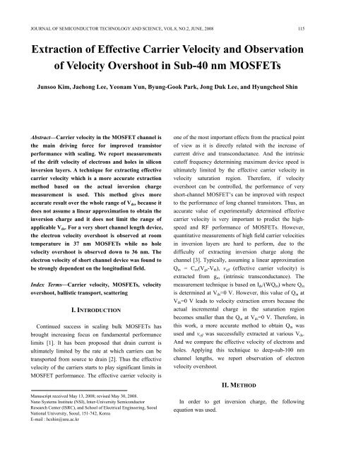
JOURNAL OF SEMICONDUCTOR TECHNOLOGY AND SCIENCE, VOL.8, NO.2, JUNE, 2008 117Q i[ fC ]Q i[ fC ]40353025201510504540353025201510501st term in equation2nd term in equationchannel chargeV GS- V TH= 0.6 VV DS= 1.0 VNMOS0 100 200 300 400 500V GS-V TH= -0.6 VV DS= -1.0 VPMOSL poly[ nm ]1st term in equation2nd term in equationchannel charge0 100 200 300 400 500L poly[ nm ]Fig. 5. Channel charge obtained from equation (1) <strong>of</strong> NMOS<strong>and</strong> PMOS.constant value. However, this formalism begins to breakdown when the carrier travel distance is scaled down.The average carrier velocity can be substantially greaterthan that expected. In other words, as the longitudinalelectric field increases, the electron gas starts to be indisequilibrium with the lattice. There is an insufficientnumber <strong>of</strong> phonon-scattering events experienced by theelectron during its flight with the result that electrons canbe accelerated to velocities higher than the saturationvelocity, thus approaching ballistic transport conditions.Extracted effective velocity <strong>of</strong> electrons <strong>and</strong> holes areplotted in Fig. 6 (a) <strong>and</strong> (b) as a function <strong>of</strong> L poly <strong>and</strong>1/L poly . The linear dependence on 1/L poly is observedespecially short channel regime. It should be noted theobtained v eff <strong>of</strong> electrons under L poly <strong>of</strong> 57 nm exceeds10 7 cm/s, indicating that the velocity overshoot isobserved. And we predict larger electron velocity asdevice dimensions continue to decrease. On the otherh<strong>and</strong>, no hole velocity overshoot is observed even at 37nm channel length. The different trend for the ratio <strong>of</strong>mobility <strong>and</strong> velocity between electrons <strong>and</strong> holes isshown in Fig. 7. In contrast to the similar rates <strong>of</strong>mobility <strong>and</strong> velocity in long channel device, there is aElectron velocity [ X10 7 cm/s ]Hole velocity [ x10 7 cm/s ]1.41.21.00.80.60.40.20.00.400.350.300.250.200.150.100.050.001/L poly[ nm -1 ]0.000 0.005 0.010 0.015 0.020 0.025 0.03NMOSV GS - V TH = 0.6 VV DS = 1.0 V0 100 200 300 400 500L poly [ nm ](a)1/L poly[ nm -1 ]0.000 0.005 0.010 0.015 0.020 0.025 0.0300.450 100 200 300 400 500L poly [ nm ](b)PMOSV GS - V TH = -0.6 VV DS = -1.0 VFig. 6. <strong>Effective</strong> carrier velocity as a function <strong>of</strong> L poly , 1/L poly .μ n/ μ p5432100 100 200 300 400 500L poly[ nm ]V ds= 1.0 VV ds= 0.5 VV ds= 0.1 VV ds= 0.01 V|V gs-V th|= 0.6 VFig. 7. The difference rate <strong>of</strong> mobility <strong>and</strong> velocity betweenelectrons <strong>and</strong> holes.disparity between mobility <strong>and</strong> velocity in short channeldevice. This is probably due to the smaller portion <strong>of</strong>gradual-channel region in short-channel MOSFETs <strong>and</strong>also easier generation <strong>of</strong> hot carriers in NMOSFETs. Fig.8 shows v eff as a function <strong>of</strong> V ds for devices with L effranging from 36 to 500 nm. It is observed that theeffective carrier velocity tends to saturate at long channeldevice <strong>and</strong> p-MOSFETs, although electron velocity543210v eff,n/ v eff,p
118 JUNSOO KIM et al : EXTRACTION OF EFFECTIVE CARRIER VELOCITY AND OBSERVATION OF …<strong>Carrier</strong> velocity [ x10 7 cm/s ]1.41.21.00.80.60.40.2|V gs-V th| = 0.6 VPMOSL poly= 37 nmL poly= 56 nmL poly= 180 nmL poly= 500 nmL poly= 36 nmL poly= 57 nmL poly= 180 nmL poly= 500 nmNMOS0.0-1.0 -0.8 -0.6 -0.4 -0.2 0.0 0.2 0.4 0.6 0.8 1.0V DS[ V ]Fig. 8. <strong>Effective</strong> carrier velocity according to the drain bias inNMOS <strong>and</strong> PMOS.overshoot occurs when the gate length is shorter than 60nm.IV. CONCLUSIONSThe electron velocity overshoot is observed while nohole velocity overshoot is observed down to 37 nmchannel length at room temperature. This indicates morefrequent scattering <strong>and</strong> heavier effective mass <strong>of</strong> holescompared with electrons. And as the longitudinal electricfield increases, there is an insufficient number <strong>of</strong>phonon-scattering events experienced by the electronduring flight with the result that electrons can beaccelerated to velocities higher than the saturationvelocity, thus approaching ballistic transport conditions.ACKNOWLEDGMENTSThis work was supported Samsung Electronics Ltd.<strong>and</strong> Nano Systems Institute.REFERENCES[1] J. B. Rldan, F. Gamiz, J. A. Lopez-Villanueva, <strong>and</strong>J. E. Carceller, “Modeling effects <strong>of</strong> electronvelocityovershoot in a MOSFET,” IEEE Transactionson Electron Devices, vol. 44, no. 5, pp. 841-846,May 1997.[2] F. Assad, Z. Ren, D. Vasileska, S. Datta, <strong>and</strong> M.Lundstrom, ”On the performance limits for SiMOSFET’s : a theoretical study,” IEEE Transactionson Electron Devices, vol. 47, no. 1, pp. 232-240,Jan. 2000.[3] J. Wang, <strong>and</strong> M. Lundstrom, “Ballistic transport inhigh electron mobility transistors,” IEEE Transactionson Electron Devices, vol. 50, no. 7, pp. 1604-1609,July 2003.[4] J. Kim, J. Lee, Y. Yun, B-G. Park, J. D. Lee, <strong>and</strong>H. Shin, “Accurate extraction <strong>of</strong> mobility, effectivechannel length, <strong>and</strong> source/drain resistance in 60nm MOSFETs,” International Conference on SolidState Devices Materials, pp. 442-443, 2007.[5] Y. Yun, I. M. Kang, B-G. Park, J. D. Lee, <strong>and</strong> H.Shin, “<strong>Extraction</strong> <strong>of</strong> effective carrier velocity inRF MOSFET,” Topical Meeting on Silicon MonolithicIntegrated Circuits in RF Systems, pp. 72-75, Jan.10-12, 2007.[6] A. Lochtefeld, <strong>and</strong> D. A. Antoniadis, “On experimentaldetermination <strong>of</strong> carrier velocity in deeply scaledNMOS : How close to the thermal limit?,” IEEEElectron Device Letters, vol. 22, no. 2, pp. 95-97,Feb. 2001.[7] F. Assaderaghi, P. K. Ko, <strong>and</strong> C. Hu, “<strong>Observation</strong><strong>of</strong> velocity overshoot in silicon inversion layers,”IEEE Electron Device Letters, vol . 14, no. 10, pp.484-486, Oct. 1993.[8] T. Mizuno <strong>and</strong> R Ohba, “Experimental study <strong>of</strong>carrier velocity overshoot in sub-0.1 μm devices -Physical Limitation <strong>of</strong> MOS structures-,” TechnicalDigest <strong>of</strong> IEDM, pp. 109-112, 1996.[9] Ritesh Gupta, S<strong>and</strong>eep Kumar Aggarwal, MridulaGupta, <strong>and</strong> R. S. Gupta, “Short channel analyticalmodel for high electron mobility transistor toobtain higher cut-<strong>of</strong>f frequency maintaining reliability<strong>of</strong> the device,” Journal <strong>of</strong> Semiconductor Technology<strong>and</strong> Science, vol. 7, no. 2, June, 2007.[10] S. Lee, “A new method to extract carrier velocityin sub-0.1- μm MOSFETs using RF measurements,”IEEE Transactions on Nanotechnology, vol. 5, no.3, pp. 163-166, May 2006.
JOURNAL OF SEMICONDUCTOR TECHNOLOGY AND SCIENCE, VOL.8, NO.2, JUNE, 2008 119Junsoo Kim was born in Korea onJuly 13, 1980. He received B.S.degree in electronic engineering fromKyunghee University, Gyunggi-do,Korea, in 2003. He is currentlypursuing the Ph.D. degree in SeoulNational University, Seoul, Korea.His major interest is deep submicrometer device modeling<strong>and</strong> characterization issues.Jaehong Lee was born in Korea onOctober 25, 1983. He received B.S.degree in electrical engineering <strong>and</strong>computer science from Seoul NationalUniversity, Seoul, Korea, in 2006,where he is currently working towardthe Ph.D. degree. His major interestis deep submicrometer device modeling <strong>and</strong> characterizationissues.Yeonam Yoon received the B.S.,M.S. degrees in electrical engineering<strong>and</strong> computer science from SeoulNational University, Seoul, Korea, in2004, 2008, respectively. In 2008 hejoined Samsung Electronics Company,Ltd., Gyunggi-do, Korea, His majorinterest is deep submicrometer device modeling <strong>and</strong>characterization issues.Byung-Gook Park received the B.S.<strong>and</strong> M.S. degrees in electronicsengineering from Seoul NationalUniversity, Seoul, Korea, in 1982<strong>and</strong> 1984, respectively, <strong>and</strong> the Ph.D.degree in electrical engineering fromStanford University, Stanford, CA, in1990. From 1990 to 1993, he was with AT&T BellLaboratories, Murray Hill, NJ, where he contributed tothe development <strong>of</strong> 0.1-μm CMOS <strong>and</strong> its characterization.From 1993 to 1994, he was with Texas Instruments,Dallas, TX, developing 0.25-μm CMOS. In 1994, hejoined the School <strong>of</strong> Electrical Engineering, SeoulNational University, as an assistant pr<strong>of</strong>essor. He iscurrently a full pr<strong>of</strong>essor. He has been in charge <strong>of</strong> theresearch <strong>of</strong> Inter-university Semiconductor ResearchCenter (ISRC) in Seoul National University since 2003as the chief <strong>of</strong> the research department. His currentresearch interests are nanoscale CMOS devices, Sisingle-electron devices, nonvolatile memory devices,<strong>and</strong> organic electroluminescent displays. Dr. Park was amember <strong>of</strong> the International Electron Devices MeetingSubcommittee on Solid State Devices from 2001 to 2002<strong>and</strong> worked for Silicon Nanoelectronics Workshop 2005as a program chair.Jong Duk Lee was born in Youngchun,Kyungpook, Korea. He received theB.S. degree in physics from SeoulNational University in 1966. Hereceived the Ph.D. degree from theDepartment <strong>of</strong> Physics at the University<strong>of</strong> North Carolina at Chapel Hill in1975. He served at the Military Communication Schoolas a ROTC <strong>of</strong>ficer from 1966 to 1968. He then worked atthe Engineering College <strong>of</strong> Seoul National University asa teaching assistant in the Department <strong>of</strong> AppliedPhysics until 1970. He was an Assistant Pr<strong>of</strong>essor in theDepartment <strong>of</strong> Electronics Engineering at KyungpookNational University from 1975 to 1978. In 1978, hestudied microelectric technology in HP-ICL at Palo Alto,CA, USA, <strong>and</strong> soon afterward worked for the KoreaInstitute <strong>of</strong> Electronic Technology (KIET) as the director<strong>of</strong> the semiconductor division. He established the KIETKumi Facility <strong>and</strong> introduced the first polysilicon gatetechnology in Korea by developing 4K SRAM, 32K <strong>and</strong>64K Mask ROM's, <strong>and</strong> one-chip 8-bit microcomputer.In July 1983, he moved to the Department <strong>of</strong> ElectronicsEngineering <strong>of</strong> Seoul National University, which hasbeen merged to School <strong>of</strong> Electrical Engineering in 1992,where he is now a Pr<strong>of</strong>essor. He started to establish theInter-University Semiconductor Research Center (ISRC)in 1985, <strong>and</strong> served as the director from 1987 to 1989.He served as the chairman <strong>of</strong> the Electronics EngineeringDepartment from 1994 to 1996. He worked for SamsungSDI Co., Ltd. as the Head <strong>of</strong> Display R&D Center for ayear on the leave <strong>of</strong> SNU in 1996. He was the member <strong>of</strong>the steering committee for IVMC(International Vacuum
120 JUNSOO KIM et al : EXTRACTION OF EFFECTIVE CARRIER VELOCITY AND OBSERVATION OF …Microelectronics Conference) from 1997-2001 <strong>and</strong> KCS(Korean Conference on Semiconductors) from 1998-2008. He was the conference chairman <strong>of</strong> IVMC´97 <strong>and</strong>KCS´98 who led the IVMC´97 <strong>and</strong> the KCS´98successfully. He was also the member <strong>of</strong> IEDM(InternationalElectron Devices Meeting) Subcommittee on Detectors,Sensors <strong>and</strong> Displays operated by IEEE Electron DevicesSociety from 1998 to 1999, he has been elected to thefirst president <strong>of</strong> the Korean Information Display Societyin June 1999 to serve until Dec.31,2001. He concentratedhis study on the image sensors such as Vidicon type,MOS type, <strong>and</strong> also CCD to help Samsung SDI Co. <strong>and</strong>Samsung Electronics Co. since 1985. His current researchinterests include sub 0.1 um CMOS structure <strong>and</strong> technology,CMOS image sensors <strong>and</strong> FED(Field Emission Display),<strong>and</strong> organic LEDs <strong>and</strong> TFTs. He published more than221 papers in the journals such as IEEE-ED <strong>and</strong> EDL,Journal <strong>of</strong> Vacuum Science <strong>and</strong> Technology, AppliedPhysics <strong>and</strong> Journal <strong>of</strong> Electrochemical Society, including160 SCI journal papers. He presented more than 361papers including 213 international conference papers. Healso registered 12 US, 4 Japanese, <strong>and</strong> 28 Korean patents.Now he is a member <strong>of</strong> IEEE, ECS, AVS, SID, KPS,KVS, IEEK, <strong>and</strong> KSS.Hyungcheol Shin received the B.S.(magna cum laude) <strong>and</strong> M.S. degreein electronics engineering from SeoulNational University, Seoul Korea, in1985 <strong>and</strong> 1987, respectively, <strong>and</strong> thePh. D. degree in electrical engineeringfrom the University <strong>of</strong> California, Berkeley, in 1993.From 1994 to 1996, he was with Motorola AdvancedCustom Technologies, as a Senior Device Engineer. In1996, he joined the Department <strong>of</strong> EECS, KAIST,Daejeon, Korea, in 1996 as an Assistant Pr<strong>of</strong>essor.During his sabbatical leave from 2001 to 2002, he waswith Berkana Wireless, CA, as a Staff Scientist in charge<strong>of</strong> CMOS RF modeling. In 2003, he joined the School <strong>of</strong>Electrical Engineering <strong>and</strong> Computer Science, SeoulNational University, Seoul, as an Associate Pr<strong>of</strong>essor. Hiscurrent research interests include RF circuits, CMOS RFmodeling, CIS, <strong>and</strong> nano CMOS. He has published over300 technical papers in international journals <strong>and</strong>conference proceedings <strong>and</strong> also wrote chapters in aJapanese book on plasma charging damage <strong>and</strong> semiconductordevice physics. Pr<strong>of</strong>. Shin was a committee memberInternational Electron Devices Meeting. He also has servedas a committee member <strong>of</strong> several international conferences,including International Workshop on Compact Modeling(IWCM) <strong>and</strong> as a committee member <strong>of</strong> IEEE EDSGraduate Student Fellowship. He is a Lifetime Member<strong>of</strong> the Institute <strong>of</strong> Electronics Engineers <strong>of</strong> Korea (IEEK)<strong>and</strong> received the Second Best Paper Award from theAmerican Vacuum Society in 1991. He also received theExcellent Teaching Award from the Department <strong>of</strong> EECSat KAIST in 1998 <strong>and</strong> from Seoul National University in2005. In 1999, he received The Haedong Paper Awardfrom the Institute <strong>of</strong> Electronics Engineers <strong>of</strong> Korea(IEEK). He is listed in Who’s Who in the World.


