System Level Architecture Evaluation and Optimization: an ... - JSTS
System Level Architecture Evaluation and Optimization: an ... - JSTS
System Level Architecture Evaluation and Optimization: an ... - JSTS
You also want an ePaper? Increase the reach of your titles
YUMPU automatically turns print PDFs into web optimized ePapers that Google loves.
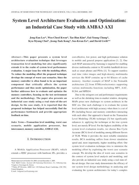
230JONG-EUN LEE et al : SYSTEM LEVEL ARCHITECTURE EVALUATION AND OPTIMIZATION: AN INDUSTRIAL...Thus we further address how to evaluate <strong><strong>an</strong>d</strong> optimize thememory controllers, focusing on our test environment <strong><strong>an</strong>d</strong>methodology. Using our architecture evaluation schemeswe could successfully find the perform<strong>an</strong>ce bottleneck <strong><strong>an</strong>d</strong>provide appropriate feedback on time to designers <strong><strong>an</strong>d</strong>system integrators.II. Design FlowFig. 1. Overall design flow from IP’s to chip layout.Fig. 2. Example system architecture.SOC designs. As a result of our system level <strong>an</strong>alysis thememory controller was found to be the single mostimport<strong>an</strong>t component that affects the overall perform<strong>an</strong>ce.Figure 1 illustrates our overall design flow startingfrom a list of IPs to chip layout. The goal of the designprocess is to determine from the given set of IPs <strong>an</strong>interconnect <strong><strong>an</strong>d</strong> memory subsystem architecture so as tomeet the perform<strong>an</strong>ce requirements. Figure 2 illustrates <strong>an</strong>example system architecture, where the IPs c<strong>an</strong> access thememory through three AHB bus layers, one AMBA3 AXI[4] interconnect, <strong><strong>an</strong>d</strong> the memory controllers. In the figurethe interconnect architecture parameters may include thenumber of AHB layers, the layer org<strong>an</strong>ization (e.g., whichIP is located in which layer), <strong><strong>an</strong>d</strong> the bus arbitrationalgorithm, while it is also conceivable to explore differentbus protocols <strong><strong>an</strong>d</strong> different memory controller algorithms.We assume that IPs c<strong>an</strong> be provided either as TLM modelsor as RTL netlists. In the case of the TLM models, IPdesign is still under way, so there may be more room forarchitectural exploration, whereas in the latter case theremay be a more restricted design space to explore. Ourmethodology c<strong>an</strong> be applied in both cases.Table. 1. Worst case scenario example (MPEG4 decoding).
JOURNAL OF SEMICONDUCTOR TECHNOLOGY AND SCIENCE, VOL.5, NO.4, DECEMBER, 2005 231III. <strong>System</strong> <strong>Level</strong> <strong>Architecture</strong><strong>Evaluation</strong>Table. 2. Perform<strong>an</strong>ce requirement example.1. Worst Case ScenarioOur system level architecture evaluation process startswith scenario definition, where a scenario c<strong>an</strong> be consideredas a refined form of perform<strong>an</strong>ce requirements. Theperform<strong>an</strong>ce requirements do not have to be detailed butshould show what will be the final perform<strong>an</strong>ce perceivedby the end user. An example of the perform<strong>an</strong>cerequirements is listed in Table 2. From the perform<strong>an</strong>cerequirements, we derive the worst case scenarios.A scenario is a set of actions played by participating IPswith (if <strong>an</strong>y) timing restrictions specified. For example, theperform<strong>an</strong>ce requirement for MPEG4 decoding states thatseveral IPs including MPEG Codec, Deblock Filter, PostProcessor, <strong><strong>an</strong>d</strong> LCD Controller should perform theiroperations at certain rates. The MPEG4 decoding scenarioc<strong>an</strong> be described as in Table 1. Note that the actiondescription part represents the test condition that needs tobe modeled, <strong><strong>an</strong>d</strong> the timing restriction part represents thetargets that should be matched by the simulation results.The action description may have “modes” (orparameters) in which each IP performs its task. Forinst<strong>an</strong>ce, the MPEG Codec is in the “decode” mode in theMPEG4 decoding scenario. Some parameters are free toch<strong>an</strong>ge, however, either by user at run time or by designerat design time. These optional parameters produce a set ofscenarios, all of which may be interesting. Preparingmodels <strong><strong>an</strong>d</strong> running simulations for all of them is a certainwaste of effort, <strong><strong>an</strong>d</strong> we prune most of the scenarios <strong><strong>an</strong>d</strong>select only the most interesting ones, those that dem<strong><strong>an</strong>d</strong>the greatest perform<strong>an</strong>ce to the system architecture (i.e.,the bus <strong><strong>an</strong>d</strong> memory controller subsystem). Those arecalled worst case scenarios.2. TLM Modeling <strong><strong>an</strong>d</strong> SimulationEvaluating the system level architecture fast <strong><strong>an</strong>d</strong>accurately is key to finding optimal interconnectarchitectures of <strong>an</strong> SOC. For the most accurate <strong>an</strong>alysisresults, the dynamic effects between various IPs, busses,<strong><strong>an</strong>d</strong> memory controllers should be taken into account. Dueto its prohibitively large computational resourcerequirement, RTL simulation is often not feasible for thiskind of system level <strong>an</strong>alysis. Also hardware emulation istoo costly <strong>an</strong> approach at the early stages of the designprocess, since the system architecture is very likely toch<strong>an</strong>ge as a result of the architecture evaluation <strong><strong>an</strong>d</strong>exploration.We use the Tr<strong>an</strong>saction <strong>Level</strong> Modeling (TLM)technique to capture the behavior of IPs, busses, <strong><strong>an</strong>d</strong>memory controllers, <strong><strong>an</strong>d</strong> to evaluate <strong><strong>an</strong>d</strong> explore differentsystem level architectures. For the most credible results,we model the components at the Bus Cycle Accurate(BCA) level of abstraction. This ensures that dynamiceffects such as bus arbitration <strong><strong>an</strong>d</strong> memory controllerscheduling are accurately reflected in our TLM simulationresults. One big drawback of the bus cycle accuratemodeling at the system level is the modeling effort. Tominimize the modeling effort we model only the IPs thatappear in the worst case scenarios. Modern MAPs consistof at least a few dozens of IPs to integrate at the top level.Modeling only a subset of the IPs is the most obvious wayto reduce the modeling effort. Further, each IP has <strong>an</strong>umber of modes <strong><strong>an</strong>d</strong> parameters. It is arguable thatmodeling <strong><strong>an</strong>d</strong> testing <strong>an</strong> IP for all its modes <strong><strong>an</strong>d</strong>parameters may require more effort th<strong>an</strong> modelingmultiple IPs for a subset of modes <strong><strong>an</strong>d</strong> parameters. Thuswe model only those features that will be used in the worstcase scenarios, which should reduce the modeling effort.Figure 3 illustrates our system architecture evaluationflow using TLM. Using the worst case scenarios we c<strong>an</strong>reduce the number of IPs <strong><strong>an</strong>d</strong> of simulation runs tominimum. The major effort is then put into (if IPs areprovided in RTL only) developing TLM models <strong><strong>an</strong>d</strong>running simulations making sure all the action description
JOURNAL OF SEMICONDUCTOR TECHNOLOGY AND SCIENCE, VOL.5, NO.4, DECEMBER, 2005 233Fig. 4. Memory controller refinement flow.Fig. 5. Memory controller test environment.found that the memory controller does not perform writeb<strong>an</strong>k interleaving even when it is signific<strong>an</strong>tlyadv<strong>an</strong>tageous. Figure 6 shows the simulation resultshighlighting the ineffective behavior of the memorycontroller. The waveform shown is for a tr<strong>an</strong>saction withthe burst size being four. In this particular case the fourtr<strong>an</strong>sfers access four different b<strong>an</strong>ks of the memory <strong><strong>an</strong>d</strong>there is no prior tr<strong>an</strong>saction that is still in execution. Thenthe ideal memory controller should issue row activationcomm<strong><strong>an</strong>d</strong>s for each of the four memory b<strong>an</strong>ks <strong><strong>an</strong>d</strong> try toexpedite the overall tr<strong>an</strong>saction, hiding the row activationlatency. However as the figure suggests, the initial memorycontroller wasn’t doing this obvious optimization. Afteridentifying the cause of the problem we could enh<strong>an</strong>ce thewrite perform<strong>an</strong>ce when write b<strong>an</strong>k interleaving c<strong>an</strong> beperformed. Figure shows the tr<strong>an</strong>saction after write b<strong>an</strong>kinterleaving is implemented in the memory controller. Inthis case the write latency is reduced from 71 cycles to 32cycles (corresponding to 45% improvement).2. Write Data FIFO MergingAnother example of improving the memory controllerperform<strong>an</strong>ce through our automatic test environment isrelated to the write data FIFO, which resides in thememory controller. To support multiple outst<strong><strong>an</strong>d</strong>ingtr<strong>an</strong>sactions the memory controller has <strong>an</strong> internal writedata FIFO. But if the write data FIFO becomes full, atr<strong>an</strong>saction with more th<strong>an</strong> one write data items wouldenter the FIFO as if it were two separate tr<strong>an</strong>sactions. Wewere able to identify this erroneous behavior using our testenvironment, as depicted in Figure 8. After removing thisinefficiency by merging the (incorrectly separated) twotr<strong>an</strong>sactions, the memory controller could perform as itshould (reducing the latency from 17 to 13 cycles, in theexample).Fig. 6. Before write b<strong>an</strong>k interleaving.Fig. 7. After write b<strong>an</strong>k interleaving.
234JONG-EUN LEE et al : SYSTEM LEVEL ARCHITECTURE EVALUATION AND OPTIMIZATION: AN INDUSTRIAL...VI. AcknowledgmentsThe authors would like to th<strong>an</strong>k Dr. Byeong Min inCAE Center, Samsung <strong><strong>an</strong>d</strong> Harry Cho in Processor<strong>Architecture</strong> Lab., Samsung for their useful comments <strong><strong>an</strong>d</strong>discussion.Fig. 8. Erroneous behavior when write data FIFO is full.ReferencesV. ConclusionsIn this paper we presented a case study designing acomplex SOC for modern mobile application processors,which typically have stringent requirements for cost,power, <strong><strong>an</strong>d</strong> perform<strong>an</strong>ce. To address the challenge of<strong>an</strong>alyzing <strong><strong>an</strong>d</strong> exploring different interconnectarchitectures in a timely m<strong>an</strong>ner with the highest accuracy,we used the TLM technique at the BCA modeling level.To reduce the high modeling effort of BCA modeling, weexploited the concept of worst case scenarios for modelingsystem level architectures. Our architecture <strong>an</strong>alysistechnique provides reliable system level perform<strong>an</strong>ceestimates taking into account dynamic effects between IPs<strong><strong>an</strong>d</strong> busses, <strong><strong>an</strong>d</strong> also enables system level architectureexploration. We also addressed how to evaluate <strong><strong>an</strong>d</strong>optimize the memory controller, which was found to be asystem level component with critical import<strong>an</strong>ce for MAPperform<strong>an</strong>ce. We demonstrated the efficacy of our designevaluation technique using a real industrial design.Applying our architecture evaluation technique we couldeasily find perform<strong>an</strong>ce bottlenecks <strong><strong>an</strong>d</strong> provideappropriate feedback to designers <strong><strong>an</strong>d</strong> system integrators.Our future work includes investigating <strong><strong>an</strong>d</strong> qu<strong>an</strong>tifyinghow much our technique c<strong>an</strong> save the modeling effort forsystem level architecture evaluation. Being based onscenarios <strong><strong>an</strong>d</strong> ultimately on perform<strong>an</strong>ce requirements, oursystem level evaluation technique is susceptive to therequirement ch<strong>an</strong>ge. An incremental method thereforewould be desirable to accommodate the perform<strong>an</strong>cerequirement ch<strong>an</strong>ge.[1] “Mobile application processor for 3G phones,” 3GNewsletter, Sept. 2004, online document available athttp://www.3g.co.uk/PR/Sept2004/8344.htm, lastaccessed July 20, 2005.[2] “New multimedia application processor chips for2.5/3G mobile phones,” 3G Newsletter, Feb. 2003,online document available at http://www.3g.co.uk/PR/Feb2003/4832.htm, last accessed July 20, 2005.[3] T. Grotker et al., <strong>System</strong> Design with <strong>System</strong>C, Kluwer,2002.[4] “AMBA AXI Protocol Specification,” ARM Limited,2003.[5] “PrimeCell AXI Configurable Interconnect,” ARMLimited, Ref: ARM DDI 0354A, Dec 2004.[6] “ARM PrimeCell Dynamic Memory ControllerTechnical Reference M<strong>an</strong>ual,” ARM Limited, Ref:ARM DDI 0331A, June 2004.[7] Specm<strong>an</strong> eVC, further information available onhttp://www.cadence.com/verisity.
JOURNAL OF SEMICONDUCTOR TECHNOLOGY AND SCIENCE, VOL.5, NO.4, DECEMBER, 2005 235Jong-Eun Lee He received a B.S. <strong><strong>an</strong>d</strong> <strong>an</strong>M.S. in electrical engineering <strong><strong>an</strong>d</strong> a Ph.D.in electrical engineering <strong><strong>an</strong>d</strong> computerscience all from Seoul NationalUniversity. He was a visiting scholar inCenter for Embedded Computer <strong>System</strong>s,University of California, Irvine during J<strong>an</strong>uary 2002 throughMarch 2003. He is currently with Design Technology Group ofSamsung SoC R&D Center in Korea. His research interestsinclude automation of embedded system design, reconfigurableprocessor architecture, <strong><strong>an</strong>d</strong> SoC on-chip interconnect.Kyu-Myung Choi He received B.S. <strong><strong>an</strong>d</strong>M.S. degrees from H<strong>an</strong>y<strong>an</strong>g University,Seoul, Korea, in 1983 <strong><strong>an</strong>d</strong> 1985,respectively <strong><strong>an</strong>d</strong> Ph.D degree in electricalengineering from the University ofPittsburgh, USA, in 1995. His Ph.Dresearch focused on the development of algorithms for CADtools on system-level design automation. Since 1985, he is withSamsung Electronics as <strong>an</strong> engineer of CAE(Computer AidedEngineering) team. He studied his Ph.D course as a Samsungscholarship. Now he is a Vice President of CAE center,<strong>System</strong>-LSI Division, Samsung Electronics.Woo-Cheol Kwon He is a researcher inCAE center, Semiconductor Division,Samsung Electronics Co., Ltd in Korea.His research interests include system-leveldesign, on-chip interconnects <strong><strong>an</strong>d</strong>algorithm design & <strong>an</strong>alysis. He receivedthe B.S. <strong><strong>an</strong>d</strong> M.S. degrees in computer science from KoreaAdv<strong>an</strong>ced Institute of Science <strong><strong>an</strong>d</strong> Technology.Tae-Hun Kim He is a researcher in CAEcenter, Semiconductor Division, SamsungElectronics Co., Ltd in Korea. His researchinterests include high-perform<strong>an</strong>cearchitecture system <strong><strong>an</strong>d</strong> high-b<strong><strong>an</strong>d</strong>widthmemory controller design. He received theB.S. degrees in electronic engineering from Inha university.Eui-Young Chung He received the PhDdegree in electrical engineering fromSt<strong>an</strong>ford University in 2002. He is aassociate professor of electrical <strong><strong>an</strong>d</strong>electronic engineering at Yonsei University,Seoul, Korea. From 1990 to 2005, he was aprincipal engineer at SoC R&D center, Samsung Electronics,Kiheung, Korea. Dr. Chung’s research interests are systemarchitecture <strong><strong>an</strong>d</strong> VLSI design including all aspects of computeraided design with the special emphasis on low power applications<strong><strong>an</strong>d</strong> in the design of mobile systems.Jeong-Taek Kong He received the B.S.degree in electronics engineering fromH<strong>an</strong>y<strong>an</strong>g University, Korea, in 1981, theM.S. degree in electronics engineeringfrom Yonsei University, Korea, in 1983,<strong><strong>an</strong>d</strong> the Ph.D. degree in electricalengineering from Duke University, Durham, NC, in 1994.From 1983 to 1990, he was with Samsung Electronics Co.,Ltd., as a VLSI CAD m<strong>an</strong>ager. From 1990 to 1994, he was atDuke University gr<strong>an</strong>ted by a Fellowship from SamsungElectronics Co., Ltd. Currently, he is with SemiconductorBusiness, Samsung Electronics Co., as VP of CAE Team. Hehas authored <strong><strong>an</strong>d</strong> coauthored more th<strong>an</strong> 110 technical papers ininternational journals <strong><strong>an</strong>d</strong> conferences <strong><strong>an</strong>d</strong> coauthored a booktitled Digital Timing Macromodeling for VLSI DesignVerification (Norwell, MA: Kluwer, 1995). His researchinterests focus on various VLSI CAD tools <strong><strong>an</strong>d</strong> designtechnologies.He has served on the program committees of IEEEInternational Workshop on Statistical Metrology, InternationalConference on VLSI <strong><strong>an</strong>d</strong> CAD, International Symposium onQuality of Electronic Design, International Conference onSimulation of Semiconductor Processes <strong><strong>an</strong>d</strong> Devices,International Workshop on Behavioral Modeling <strong><strong>an</strong>d</strong>Simulation, International Symposium on Low PowerElectronics <strong><strong>an</strong>d</strong> Design, International SOC Design Conference,<strong><strong>an</strong>d</strong> International Electron Devices Meeting. He is a Memberof N<strong>an</strong>oelectronics <strong><strong>an</strong>d</strong> Giga-Scale <strong>System</strong>s (NaGS) TechnicalCommittee <strong><strong>an</strong>d</strong> serves as a Distinguished Lecturer for the IEEECircuits <strong><strong>an</strong>d</strong> <strong>System</strong>s Society. He was <strong>an</strong> Associate Editor ofIEEE Tr<strong>an</strong>sactions on Circuits <strong><strong>an</strong>d</strong> <strong>System</strong>s-II <strong><strong>an</strong>d</strong> IEEE
236JONG-EUN LEE et al : SYSTEM LEVEL ARCHITECTURE EVALUATION AND OPTIMIZATION: AN INDUSTRIAL...Tr<strong>an</strong>sactions on Very Large Scale Integrated (VLSI) <strong>System</strong>s<strong><strong>an</strong>d</strong> was nominated as a member of IMEC Scientific AdvisoryBoard in Belgium in 2004.Soo-Kw<strong>an</strong> Eo He has been senior vicepresident of Samsung Electronics’ SoCR&D Center focusing on the ESL Designsince late 2002. He currently directs the teamthat deals in SoC on-chip communicationsfabrications including NoC <strong><strong>an</strong>d</strong> pre-siliconSoC solution development methodology. His team developed theSamsung’s Virtual Platform, called ViP, low power architecturedesign technology, HW/SW co-design technology, <strong><strong>an</strong>d</strong> SamsungSoC bus architecture. He played a key role to deploy these ESLdesign technologies within comp<strong>an</strong>ies. Mr. Eo received MS inECE from the University of Arizona Tucson, Arizona in 1986 <strong><strong>an</strong>d</strong>had worked in various comp<strong>an</strong>ies including Cadence, Synopsys,Intel, VIA Technologies in S<strong>an</strong> Jose, California for 16 years beforehe joined the Samsung.Dave Gwilt He is the engineering m<strong>an</strong>agerfor the Fabric IP Business Unit of ARM inCambridge. His industrial experienceincludes development of the ARM920T <strong><strong>an</strong>d</strong>ARM1136JS processors, <strong><strong>an</strong>d</strong> architecture ofthe PL340 family of SDRAM controllers<strong><strong>an</strong>d</strong> PL330 family of DMA controllers. His technology interestsinclude tr<strong>an</strong>saction-level modeling of IP. He received a Mastersdegree in engineering from Cambridge University.


