A Delta-Sigma Fractional-N Frequency Synthesizer for Quad ... - JSTS
A Delta-Sigma Fractional-N Frequency Synthesizer for Quad ... - JSTS
A Delta-Sigma Fractional-N Frequency Synthesizer for Quad ... - JSTS

You also want an ePaper? Increase the reach of your titles
YUMPU automatically turns print PDFs into web optimized ePapers that Google loves.
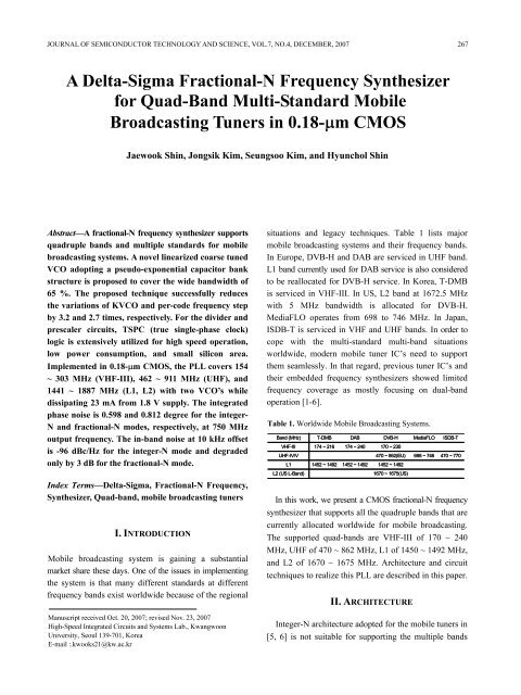
268 JAEWOOK SHIN et al : A DELTA-SIGMA FRACTIONAL-N FREQUENCY SYNTHESIZER FOR~AFC6V DDTCXO/RfRf VPFD/CPOff-chipVDD/2LOGEN/2/2/6L1 & L2UHFVHFIIIV REFRegulatingAm plifierR 5C 5M 5L 1C 1ProgrammableDFF Prescaler /2CounterM 3 M 4DSML tankFig. 1. <strong>Frequency</strong> synthesizer architecture.and multiple standards. There<strong>for</strong>e, fractional-N architecturewith a third-order multi-bit delta sigma modulator(DSM) is realized. Fig. 1 shows the PLL architecture.Two VCO’s cover the quad-band; a high-band VCO(VCOH) covering 2900 ~ 3350 MHz and a low-bandVCO (VCOL) covering 940 ~ 1724 MHz. LOGENblock generates LO signals, in which the divide-by-6 isused <strong>for</strong> the VHF band and the divide-by-2’s are used <strong>for</strong>L1/L2 and UHF bands. These divider circuits are basedon the current-mode logic (CML) DFF <strong>for</strong> simple I/Qgeneration. Meanwhile, the divide-by-2 and the 4/5 dualmodulusprescaler in the feedback path are designed byutilizing true-single-phase-clock (TSPC) logic. A DFFafter the programmable counter synchronizes its outputto the prescaler output. This re-timing block significantlyeliminates the accumulated phase noise created by theasynchronous programmable counter. Automatic frequencycontrol (AFC) block is based on the pulse-counting andcomparison method. The number of the pulse-countingand comparison operation is programmable so that thelock time can be optimized. Typical AFC search time <strong>for</strong>the 6-bit coarse tuning is less than 150 μsec. A thirdorder loop filter is used, of which only three componentsare implemented off chip.III. BUILDING BLOCK DESIGN3.1 Wideband VCO with Linearized Coarse TuningFig. 2 shows the VCO circuit schematic. A regulatingamplifier is employed to reduce the power supplysensitivity of the VCO and thereby its phase noisecontribution. Reference voltage V REF is generated by areplica circuit with a bandgap reference current. Thesimulated output noise of the bandgap circuit is 12.2 and10.9 nV/√Hz at 100 kHz and 1 MHz, respectively. A lowpass filter of R 5 and C 5 is employed to further suppressthe noise transferred from the regulator.Fig. 2. VCO circuit schematic.Cap. BankM 1 M 2Conventional binary weighted cap bank is utilized <strong>for</strong>the VCOH whose fractional bandwidth is about 25 %.However, <strong>for</strong> the VCOL whose fractional bandwidth isover 70 % considering PVT variations, the conventionalcap bank cannot be used due to the extremely widetuning range. The K VCO and the frequency step per a capbank code vary over 10 times. Such a big K VCO variationmakes difficult optimal design of the PLL loopcharacteristics, possibly leading to severe degradation ofphase noise and lock time in some channels. The bigvariation of the per-code frequency step also prohibitsoptimal design of AFC search time because the numberof pulse-counting must be set unnecessarily high enoughto detect the smallest frequency step. Hauspie et al.proposed a combined tuning technique of capacitor bank,varactor, and active core size to address these problems[7]. However, we found that the method showed verylimited effects <strong>for</strong> such a wide bandwidth of this workdue to the conventional binary-weighted cap bank structure.Here we propose a novel pseudo-exponential cap bankstructure. Fig. 3 shows the structure. It consists of a subsectioncap bank, a variable-slope linear cap bank, and a varactorbank. Fig. 4 illustrates the effects of the proposed capbank by comparing the coarse tuning characteristics thatcan be obtained by the proposed and the conventionalcap bank structures. Since the VCO output frequency isdetermined by 1/(2π√LC), it would be ideal to make thetotal capacitance of a cap bank vary in an exponential<strong>for</strong>m of n -2 with respect to the cap bank code n. However,this is not practical <strong>for</strong> real implementation because of theL 2
JOURNAL OF SEMICONDUCTOR TECHNOLOGY AND SCIENCE, VOL.7, NO.4, DECEMBER, 2007 26955 5CLK432242(a)Fig. 3. Pseudo-exponential capacitor bank structure.CLKD Q D QMCOUTDQ(b)Fig. 5. (a)TSPC divide-by-2 circuit and (b) TSPC 4/5 prescalerlogic diagram.LSB 20A3IN23MSB 33-bitAdd24-bitAdd24-bitReg24-bitAdd24-bitReg24-bitAdd24-bitRegA226-bitAdd3OUTA1(a)Fig. 4. Comparison of coarse tuning characteristics by theconventional binary-weighted cap bank and the proposedpseudo-exponential cap bank structure. (a) <strong>Frequency</strong> tuningcharacteristics. (b) <strong>Frequency</strong> and K vco variation against the capbank tuning code at a fixed V tune .20IN20-bitadderError Cancellation Network andMapping LogicC1C220-bitadderC320-bitadder3OUTextremely huge ratio of the maximum and minimumcapacitances (e.g. 64 2 <strong>for</strong> 6-bit coarse tuning in VCO).Thus, we mimic the n -2 -dependency by using apseudo-exponentially varying capacitance. As shown inFig. 4, the total tuning range is divided into foursubsections (B n ). Within each subsection, capacitancevaries linearly with a different slope. The slope isdetermined by the different unit capacitance whichvaries from 1⋅C unit to 3⋅C unit in each subsection. Duringthe inter-subsection transitions, the cumulative capacitanceis re-adjusted in the subsection cap bank to make the totalcapacitance vary smoothly. Also, the varactor capacitance isadjusted in each subsection by the varactor bank in orderto keep the K VCO constant. This proposed structure isadopted <strong>for</strong> the wideband VCOL, which is referred to asVCOL-LCT. By using this structure, the coarse tuningcharacteristics are dramatically linearized.CLK20-bitregister20-bitregister(b)20-bitregisterFig. 6. Logic block diagram of designed delta-sigma modulatorswith 20-bit resolution. (a) 3 rd -order 3-bit single-loop CIFF and(b) MASH-111.3.2 Divide-by-2, 4/5-Prescaler, and PFD in TSPC logicThe divide-by-2 and 4/5 dual-modulus prescaler in thefeedback path are realized in the TSPC logic. Fig. 5(a)shows the circuit schematic of the divide-by-2, where theFET widths are shown while the gate length is minimum0.18 μm. The widths are optimized <strong>for</strong> high speed operationand large swing by trading off the self-capacitance andthe driving capability. The same DFF is also used <strong>for</strong> thedual-modulus prescaler, whose circuit is shown in Fig.5(b). In the simulation, the maximum operation frequenciesof the divide-by-2 and the prescaler are 6 GHz and 3.5
270 JAEWOOK SHIN et al : A DELTA-SIGMA FRACTIONAL-N FREQUENCY SYNTHESIZER FOR~GHz in the worst condition, while they goes up to 9 GHzand 4.5 GHz in the typical condition. Moreover, thecurrent consumption of the prescaler is only 0.8 mA. Wehave found that the TSPC logic dramatically reduces thepower consumption and silicon area compared to theconventional CML logic. The TSPC logic DFF is alsoused in the PFD circuit in order to minimize the timingmismatch of the UP/DN pulses.3.3 <strong>Delta</strong>-<strong>Sigma</strong> ModulatorIn general, DSM poses significant impacts on thephase noise per<strong>for</strong>mance of the PLL. We implement twotypes of DSM: a 3 rd -order 3-bit single-loop DSM ofCIFF (cascaded integrators with distributed feed<strong>for</strong>ward)type which is similar to that in [8] and MASH-111 with20-bit resolution. Fig. 6 shows the block structures ofsingle-loop modulator and MASH-111. In single-loopmodulator, the coefficients A 1 , A 2 , and A 3 are 2, 1.5, and0.5, respectively. Fig. 7 shows the simulated PSDs (powerspectral density) of each modulator. It is clearly seen thatboth are non-tonal. Fig. 8 compares NTFs (noise transferfunction) of MASH-111 and single-loop modulator. Itclearly exhibits the great difference of the NTF’s of thetwo DSMs. According to the linear analysis results, themaximum and integral quantization noises of the implementedsingle-loop architecture are found to be considerably lessthan the conventional MASH-111 structure, only about40 % and 28 %, respectively. Time-domain simulation isalso per<strong>for</strong>med to examine the dynamic range. Fig. 9shows the internal node values in the DSM with respectto the input value. As can be seen, the dynamic range ofMagnitude (dB)0-50-100-150MASHSingleLoop-20010 -3 10 -2 10 -1Normalized <strong>Frequency</strong> (Hz)Fig. 7. Simulated power spectral density of MASH-111 andsingle-loop delta-sigma modulators.this architecture is about -2.5 ~ +2.0, which is significantlylarger than the conventional MASH-111 whose dynamicrange is only -0.5 ~ +0.5. The time-domain simulationalso shows the number of output levels is only about 4while that of the MASH-111 is 8, possibly leading toless noise folding and lower in-band noise. For theseadvantages, the single-loop CIFF architecture is chosenin this work.IV. MEASUREMENT RESULTSThe frequency synthesizer was fabricated in a 0.18-μm RF CMOS process. Fig. 10 shows the chip micrograph.The die area is 2.5×2.5 mm 2 . It is packaged in a 40-pinleadless plastic chip carrier (LPCC) and tested on anevaluation printed circuit board with a 1.8-V supply. Itdissipates 21 mA <strong>for</strong> UHF/L1/L2 bands and 23 mA <strong>for</strong>VHF band. The slight additional currents at VHF band isconsumed by the divider-by-6 in the LOGEN block.|NTF(z)|8642MASHSingleLoop00.0 0.1 0.2 0.3 0.4 0.5Normalized <strong>Frequency</strong> (Hz)Fig. 8. Noise transfer function of MASH-111 and single-loopdelta-sigma modulators.SL Internal Node Values20151050-5-10-15-20-4 -2 0 2Input ValueFig. 9. Dynamic range simulation of the single-loop delta-sigmamodulator.
JOURNAL OF SEMICONDUCTOR TECHNOLOGY AND SCIENCE, VOL.7, NO.4, DECEMBER, 2007 271Fig. 10. Chip micrograph.<strong>Frequency</strong> (MHz)19001800170016001500140013001200110010009000.0 0.3 0.6 0.9 1.2 1.5 1.8Tuning Voltage (V)0.0 0.3 0.6 0.9 1.2 1.5 1.8(a)(b)Fig. 12. Measured frequency tuning characteristics of the lowband VCO with (a) the proposed pseudo-exponential cap bankand (b) the conventional binary weighted cap bank.<strong>Frequency</strong> (MHz)380036003400320030002800180016001400120010008000.0 0.2 0.4 0.6 0.8 1.0 1.2 1.4 1.6 1.8Tuning Voltage (V)Fig. 11. Measured frequency tuning characteristics of the lowbandand high-band VCO’s.Fig. 11 shows the measured frequency tuning rangesof the VCOH and VCOL-LCT which are 2882 ~ 3775MHz and 924 ~ 1823 MHz, respectively. They successfullycover the target ranges. The measured phase noises are -90 dBc/Hz at 100 kHz offset and -122 dBc/Hz at 1.45MHz offset <strong>for</strong> the 3 GHz output frequency in theVCOH, and -110 dBc/Hz at 100 kHz offset and -135dBc/Hz at 1.45 MHz offset <strong>for</strong> the 1-GHz outputfrequency in the VCOL-LCT.In order to examine the effects of the proposed pseudoexponentialcap bank structure, a test VCO with theconventional cap bank structure is also fabricated andcompared. Fig. 12 shows the measured coarse tuningcharacteristics of VCOL and VCOL-LCT. For the VCOL,the ranges of the K VCO and the frequency step are 23 ~123 MHz/V and 5 ~ 29 MHz/code, respectively. For theVCOL-LCT, they are reduced to 37 ~ 72 MHz/V and 9 ~16 MHz/code at V tune = 0.9 V. Thus the variation of(a)(b)Fig. 13. PLL phase noise measurement. (a) Integer-N mode at825.6 MHz. (b) <strong>Fractional</strong>-N mode at 827.5 MHz.K VCO is reduced from 530 % to 190 % and the variationof the frequency step is reduced from 580 % to 180 %.They correspond to 3.2- and 2.7-times reduction, respectively.Fig. 13 shows the measured phase noise of the PLL. Inthe measurement, the loop bandwidth is 70 kHz, thereference frequency is 19.2 MHz, and the charge pumpcurrent is 2 mA. Fig. 13(a) is <strong>for</strong> the integer-N modewith the output frequency of 825.6 MHz and Fig. 13(b)is <strong>for</strong> the fractional-N mode with the output frequency of827.52 MHz where the DSM output value is +0.1. Thein-band noise at 1 kHz is -95 dBc/Hz <strong>for</strong> the integer-Nmode and becomes -91.2 dBc/Hz <strong>for</strong> the fractional-Nmode, which is only 3.8-dB degradation. The phasenoises at 100 kHz and 1.45 MHz offsets are -101.7 and -132.9 dBc/Hz <strong>for</strong> the integer-N mode, and -100.9 and -130.9 dBc/Hz <strong>for</strong> the fractional-N mode. In the fractional-
272 JAEWOOK SHIN et al : A DELTA-SIGMA FRACTIONAL-N FREQUENCY SYNTHESIZER FOR~N mode, residual quantization noise is slightly observedat around 2 MHz offset. Integrated phase noise is acrucial factor affecting the signal-to-noise ratio in OFDMsignal. The phase noise integrated from 1 kHz to 3.8MHz is measured to be 0.807 degree (-37.0 dBc) and0.910 degree (-35.9 dBc) <strong>for</strong> the integer-N and fractional-Nmodes, respectively. At lower output frequencies, thephase noise per<strong>for</strong>mances become better. For instance, atan output frequency of 500 MHz, the integrated phasenoise is measured to be 0.145 and 0.244 degree <strong>for</strong> theinteger-N and fractional-N modes, respectively. It successfullymeets the DVB-H requirement of -33 dBc [5]. Meanwhile,the reference and fractional spur are measured to be lowerthan -70 dBc and -50dBc, respectively. The lock time ismeasured to be less than 150 μsec including the 6-bitAFC search time.V. CONCLUSIONSTV Tuner IC <strong>for</strong> T-DMB/DAB and ISDB-T,”ISSCC Dig. Tech. Papers, pp.614-615, Feb. 2006.[5] P. Antoine et al., “A Direct-Conversion Receiver <strong>for</strong>DVB-H,” IEEE J. Solid-State Circuits, vol. 40, no. 2,pp. 2536-2546, Dec. 2005.[6] M. Marutani et al., “An 18mW 90 to 770 MHz<strong>Synthesizer</strong> with Agile Auto-Tuning <strong>for</strong> Digital TV-Tuners,” ISSCC Dig. Tech. Papers, pp.192-193, Feb.2006.[7] D. Hauspie et al., “Wideband VCO withSimultaneous Switching of <strong>Frequency</strong> Band, ActiveCore and Varactor Size,” ESSCIRC Dig. Tech.Papers, pp.452-455, Sep. 2006.[8] W. Rhee et al., “A 1.1-GHz CMOS <strong>Fractional</strong>-N<strong>Frequency</strong> <strong>Synthesizer</strong> with 3-bit Third Order Σ-ΔModulator,” IEEE J. Solid-State Circuits, vol. 35,no. 10, pp. 1453-1460, Oct. 2000.A CMOS fractional-N frequency synthesizer to supportthe quadruple bands and multiple standards <strong>for</strong> mobilebroadcasting systems has been presented. The novellinearized coarse tuned VCO with a pseudo exponentialcapacitor bank structure is proposed to cover the widebandwidth. Implemented in 0.18-μm CMOS technology,the PLL successfully covers 154 ~ 303 MHz (VHF), 462~ 911 MHz (UHF), and 1441 ~ 1887 MHz (L1, L2) withsatisfactory phase noise per<strong>for</strong>mances.ACKNOWLEDGMENTSThis work was supported by Seoul Research andBusiness Development Program (GR070039).Jaewook Shin received B.S. andM.S. degrees in department of wirelesscommunications engineering fromKwangwoon University, Seoul, Korea,in 2004 and 2006 respectively. Hehas been a Research Assistant workingtoward the Ph.D. degree at High-Speed Integrated Circuit and System Laboratory (HICSL),Kwangwoon University, since 2007. His current researchis focused on the RF/Analog Integrated Circuits andSystems.REFERENCES[1] I. Vassiliou et al., “A 0.18um CMOS Dual-BandDirect-Conversion DVB-H Receiver,” ISSCC Dig.Tech. Papers, pp.606-607, Feb. 2006.[2] Y. Kim et al., “A Multi-Band Multi-Mode CMOSDirect Conversion DVB-H Tuner,” ISSCC Dig. Tech.Papers, pp.608-609, Feb. 2006.[3] M. Womac et al., “Dual-Band Single-Ended-InputDirect-Conversion DVB-H Receiver,” ISSCC Dig.Tech. Papers, pp.610-611, Feb. 2006.[4] B. Kim et al., “A 100mW Dual-Band CMOS Mobile-Jongsik Kim was born in Korea in1978. He received B.S. and M.S.degree in electrical engineering fromKwangwoon University in 2005 and2007, respectively. He is currentlyworking toward a Ph.D. degree atthe same university. His researchinterests are wide-band transmitter and linearizationmethod <strong>for</strong> medium power amplifiers in CMOS technology.
JOURNAL OF SEMICONDUCTOR TECHNOLOGY AND SCIENCE, VOL.7, NO.4, DECEMBER, 2007 273Seungsoo Kim was born in Korea in1976. He received B.S. and M.S.degree in electrical engineering fromGunsan University, Gunsan, Korea,in 1998 and Kwangwoon University,Seoul, Korea, in 2004 respectively.He is presently working towards hisPh.D. degree at High-Speed Integrated Circuit andSystem Laboratory (HICSL), Kwangwoon University,since 2004. His current research is the RF/AnalogIntegrated Circuits and Systems in CMOS technology.Hyunchol Shin received B.S., M.S.and Ph.D. degrees in electricalengineering from Korea AdvancedInstitute of Science and Technology(KAIST), Daejon, Korea, in 1991,1993 and 1998, respectively. In 1997,he worked at Daimler Benz ResearchCenter, Ulm, Germany as a doctoral research student.From 1998 to 2000, he was with Samsung Electronics asa Senior RF/Analog IC Design Engineer, where he wasinvolved in the RF/IF chipset development <strong>for</strong>CDMA/AMPS mobile handsets. In April 2000, he joinedthe Electrical Engineering Department of the Universityof Cali<strong>for</strong>nia, Los Angeles as a Postdoctoral ResearchAssociate, where he had worked on RF transceiverdesign using CMOS and SiGe BiCMOS. He also servedas a Lecturer at UCLA teaching Analog ElectronicCircuits <strong>for</strong> undergraduate students. In May 2002, hejoined Qualcomm RF/Analog IC design group as aSenior Engineer, where he had been involved in thedevelopment of multi-band multi-mode GSM/WCDMAtransceivers. Since September 2003, he has been with theDepartment of Radio Science and Engineering,Kwangwoon University, Seoul, Korea, where he iscurrently an Associate Professor. His research interestsare RF/Analog/Microwave Integrated Circuits andSystems.