Lab 3: Advanced ASIC Design Flow - Sm.luth.se
Lab 3: Advanced ASIC Design Flow - Sm.luth.se
Lab 3: Advanced ASIC Design Flow - Sm.luth.se

You also want an ePaper? Increase the reach of your titles
YUMPU automatically turns print PDFs into web optimized ePapers that Google loves.
Instructions for<strong>Lab</strong> 3: <strong>Advanced</strong><strong>ASIC</strong> <strong>Design</strong> <strong>Flow</strong>SMD154 VLSI <strong>Design</strong>
SMD154 VLSI <strong>Design</strong><strong>Lab</strong> 3: <strong>Advanced</strong> <strong>ASIC</strong> <strong>Design</strong> <strong>Flow</strong>1 SCAN CHAIN ......................................................................................................31.1 SCAN CHAINS AND DESIGN FOR TEST.............................................................32 LAB ASSIGNMENT 3A......................................................................................42.1 CHECKING YOUR SCAN CHAIN .......................................................................42.2 SUBMISSION 3A...............................................................................................43 LAB ASSIGNMENT 3B......................................................................................53.1 CHECKING THE SCAN CHAIN...........................................................................53.2 SUBMISSION 3B...............................................................................................64 LAB ASSIGNMENT 3C......................................................................................64.1 DESIGN ENTRY ...............................................................................................64.2 FRONTEND - CHANGED CLOCK FREQUENCY...................................................74.3 BACKEND........................................................................................................74.4 VERIFY ...........................................................................................................84.5 POST LAYOUT SIMULATION ............................................................................85 APPENDIX.........................................................................................................102(10)
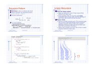
SMD154 VLSI <strong>Design</strong><strong>Lab</strong> 3: <strong>Advanced</strong> <strong>ASIC</strong> <strong>Design</strong> <strong>Flow</strong>1 Scan Chain1.1 Scan Chains and <strong>Design</strong> for TestIn this lab you will continue to work with your ALU design from lab 2. A simpledirectory structure (with a modified test bench) can be found at/digcad/smd154/2006/lab3/lab3.zip.You will get an introduction to DFT (design for test) by in<strong>se</strong>rting a scan chain intoyour design and <strong>se</strong>e which fault cover you can reach. A common technique u<strong>se</strong>d forDFT (design for test) is an internal scan chain. Complex <strong>se</strong>quential blocks arepartitioned in either isolated combinational blocks (full-scan design) or partiallyisolated combinational blocks (partial-scan design). By extending the flip-flops withsupport for <strong>se</strong>rial shift (compare DFC1 with DFSEC1); it is possible to chain the flipflopstogether to form a scan-chain (Figure 1).Figure 1. Example of a design without and with a scan chain.Synopsys u<strong>se</strong>s DFT Compiler to in<strong>se</strong>rt scan chains into the design. There are a fewdifferent scan methods available and the one u<strong>se</strong>d in this lab is called multiplexedflip-flop (Figure 2). A drawback with this method is that the performance of thecircuit is decrea<strong>se</strong>d. In short, the multiplexed flip-flop scan style u<strong>se</strong>s a multiplexeddata input to provide <strong>se</strong>rial shift capability. During functional mode, the scan-enablesignal, acting as the multiplexer <strong>se</strong>lect line, <strong>se</strong>lects the system data input. During scanshift, the scan-enable signal <strong>se</strong>lects the scan data input. The scan data input comesfrom either the scan input port or the scan output pin of the previous cell in the scanchain.Figure 2. Multiplexed flip-flop scan cell.Read more about scan chains in chapter 14.6 in <strong>Sm</strong>ith, Application-SpecificIntegrated Circuits (http://www.edacafe.com/books/<strong>ASIC</strong>/Book/CH14/).3(10)
SMD154 VLSI <strong>Design</strong><strong>Lab</strong> 3: <strong>Advanced</strong> <strong>ASIC</strong> <strong>Design</strong> <strong>Flow</strong>2 <strong>Lab</strong> assignment 3aThis lab is an introduction to DFT flows for designs in the logical domain, thus wewill only u<strong>se</strong> <strong>Design</strong> Compiler and Synopsys DFT compiler. In this lab assignment3a, u<strong>se</strong> the same vhdl-files as in the previous lab, and feel free to reu<strong>se</strong> the same scriptfor logical synthesis as you u<strong>se</strong>d before. Plea<strong>se</strong> <strong>se</strong>e Appendix for using the command<strong>se</strong>quence provided, where you can take a design from an HDL-level circuitdescription (without existing scan) to a fully optimized design with internal scancircuitry.2.1 Checking Your Scan ChainFault coverage is a method to define testability of a design and shows to what extentthe design can be checked for manufacturing defects. Fault coverage is defined asfault coverage = detected faults / detectable faultsRead more in chapter 14.1 and 14.1 in <strong>Sm</strong>ith, Application-Specific Integrated Circuits(http://www.edacafe.com/books/<strong>ASIC</strong>/Book/CH14/). As noted in the appendix,you u<strong>se</strong> the command estimate_test_coverage to check your fault coverage andu<strong>se</strong> the command dft_drc to check your design against the design rules formultiplexed flip-flop. You should not have any (dft) violations in assignment 3a.2.2 Submission 3aAs indicated in the script in the appendix, after the scan in<strong>se</strong>rtion, you need toperform design rule checking again to ensure no violations have been introduced intoyour design by the scan in<strong>se</strong>rtion process. More specifically, you execute and save ina text file (lab3a.txt) the results of the commands:# Check that you have satisfied the constraintsreport_constraint -all_violators -verbo<strong>se</strong># Recheck the test design rulesdft_drc# Report scan pathreport_scan_path -view existing_dft -chain all# Check test coverage statistics on the current designestimate_test_coverage# Report max/min delayreport_timing -path full -delay minreport_timing -path full -delay maxIn the same text file, answer the following questions (info can be found by thegenerated report above):1. What is your max and min slack?2. What is the length of the scan path?3. What is the test coverage (%)?4. You should not have any design rule violations, but in this state, you mighthave timing problems (if so given by the report_constraint command).If you have timing violations, plea<strong>se</strong> explain as good as you can whySynopsys report violations.4(10)
SMD154 VLSI <strong>Design</strong><strong>Lab</strong> 3: <strong>Advanced</strong> <strong>ASIC</strong> <strong>Design</strong> <strong>Flow</strong>3 <strong>Lab</strong> assignment 3bYou should now discard the naive VHDL model of the SRAM that was given in lab 2since it takes to long time to synthesize (that is why its size was only 16x8 bits) and,more important, it does not u<strong>se</strong> real estate (chip area) efficiently. Instead you will u<strong>se</strong>an IP block that has been pre-generated by a memory compiler from AMS (theinterested can find more information at http://asic.austriamicrosystems.com/databooks/digital/). The size of the new SRAM is 128x8 bits.You should replace the src/sram.vhd file with the sram128x8 block. In effect, it isdone already by the given .synopsys_dc.<strong>se</strong>tup that adds the path to thesram128x8.db. However, you need to modify alu.vhdl slightly to instantiatesram128x8 instead of the vhdl-file and change the number of address bits to thememory.(Note: The timing diagram for the pre-generated memory differs from the oneprovided in lab 2. In lab assignment 3b, ignore the discrepancy. For now, it is onlyrequired to change the address bits and component to instantiate).You should then be able <strong>se</strong>e to u<strong>se</strong> the same command <strong>se</strong>quence provided inappendix, where you can take a design from an HDL-level circuit description (withoutexisting scan) to a fully optimized design with internal scan circuitry. (Remember: Donot analyze src/sram.vhd. in lab assignment 3b!)3.1 Checking the Scan ChainU<strong>se</strong> the command dft_drc to check your design against the design rules formultiplexed flip-flop. Unfortunately, the three state buffers u<strong>se</strong>d by the IP blockcau<strong>se</strong>s violations.-----------------------------------------------------------------Begin Topology violations...Warning: Three-state net alu0/Q_i[7] is not properly driven.Information: There are 7 other nets with the same violation.Topology violations completed...-----------------------------------------------------------------It is possible to work around this problem using Shadow LogicDFT to create awrapper around the memory. However, we accept the<strong>se</strong> violations in this lab.Thus, your report will likely look something like this:-----------------------------------------------------------------DRC ReportTotal violations: 9-----------------------------------------------------------------1 MODELING VIOLATION1 Cell has unknown model violation (TEST-451)8 TOPOLOGY VIOLATIONS8 Improperly driven three-state net violations (TEST-115)Warning: Violations occurred during test design rule checking.-----------------------------------------------------------------Sequential Cell Report0 out of 75 <strong>se</strong>quential cells have violations-----------------------------------------------------------------SEQUENTIAL CELLS WITHOUT VIOLATIONS* 75 cells are valid scan cells5(10)
SMD154 VLSI <strong>Design</strong><strong>Lab</strong> 3: <strong>Advanced</strong> <strong>ASIC</strong> <strong>Design</strong> <strong>Flow</strong>3.2 Submission 3bAs indicated in the script in the appendix, after the scan in<strong>se</strong>rtion, you need toperform design rule checking again to ensure no violations have been introduced intoyour design by the scan in<strong>se</strong>rtion process. More specifically, you execute and save ina text file (lab3b.txt) the results of the commands:# Check that you have satisfied the constraintsreport_constraint -all_violators -verbo<strong>se</strong># Recheck the test design rulesdft_drc# Report scan pathreport_scan_path -view existing_dft -chain all# Check test coverage statistics on the current designestimate_test_coverage# Report max/min delayreport_timing -path full -delay minreport_timing -path full -delay maxIn the same text file, answer the following questions (info can be found by thegenerated report above):1. What is your max and min slack?2. What is the length of the scan path?3. What is the test coverage (%)?4. If the test coverage differs from assignment 3a, plea<strong>se</strong> explain as good as youcan why there is a difference.5. You should not have any design rule violations, but in this state, you mighthave timing problems (if so given by the report_constraint command).If you have timing violations, plea<strong>se</strong> explain as good as you can whySynopsys report violations.4 <strong>Lab</strong> assignment 3cIn this lab assignment, we will u<strong>se</strong> the IP block that has been pre-generated by amemory compiler from AMS and incorporates the block into the ALU and take thedesign through the entire design flow. In lab assignment 3c, you don’t have to in<strong>se</strong>rtscan chains into the design.4.1 <strong>Design</strong> EntryAs in assignment 3b, you should replace the src/sram.vhd file with the sram128x8block. As mentioned, the timing diagram for the pre-generated memory differs fromthe one provided in lab 2, which means that you might have redesign your ALUslightly. The timing diagram for the pre-generated memory can be found at http://asic.austriamicrosystems.com/databooks/digital/mc_spram_c35_timing.html.4.1.1 RTL SimulationRemember to compile the new memory file when simulating your design. Whensimulating the design at RTL, u<strong>se</strong> the sram128x8_func.v (that has disabled timingchecks) e.g. do:6(10)
SMD154 VLSI <strong>Design</strong><strong>Lab</strong> 3: <strong>Advanced</strong> <strong>ASIC</strong> <strong>Design</strong> <strong>Flow</strong>ncvlog /digcad/smd154/2006/lab1/sram128x8/sram128x8_func.vinstead of ncvhdl sram.vhdl.4.2 Frontend - Changed Clock FrequencyWhen the ALU is operated at a clock frequency of 100 MHz, the CMOS technologyis far from pushed to its limit. However, in this assignment, we decrea<strong>se</strong> the clockfrequency to 60 MHz instead. The rationale is that you might get hold-time violationsin your design, so when performing optimization, you can focus on fixing the holdproblems.You have to make changes in the following files:• Syntesis script1: Create clock with the new period to reflect yourfrequency.• Syntesis script2: Change the operating conditions, as max condition, <strong>se</strong>tWORST from the c35_CORELIB (instead of WORST-MIL as in lab 2).• check_layout.tcl: Change the FREQUENCY variable.4.3 BackendThe following <strong>se</strong>ttings have to be modified for Encounter:• c35b4_std.conf: Add path to sram block:tlf: /digcad/smd154/2006/lab1/sram128x8/sram128x8_43.tlflef: /digcad/smd154/2006/lab1/sram128x8/sram128x8.lefSome hints on gemma.tcl. You have to add commands for placing the memoryblock, create power rings, and cutting rows around it.• UPDATE! It <strong>se</strong>ems like the generated layout script generates a lot ofviolations when adding periphery cells. So before routing the pad ring(“srouting” gnd3o! gnd3r! vdd3o! vdd3r2! vdd3r1!), execute the fillperi.tclscript. E.g. the simplest way <strong>se</strong>ems to be: add core rings, block rings, andstripes as usual, then:> source fillperi.tcl> sroute -jogControl {preferWithChanges differentLayer}to connect all power and ground rings, block pins, pad pins, pad rings, stripes,etc. Then continue with placement of standard cells as usual.• Should you have large timing violations, consider a lower core utilizationwhen initializing the floorplan (e.g. by testing going from 85% -> 75 %)• Place the memory block. (help modulePlace)• Set block status to “fixed” and add a halo to the block, u<strong>se</strong>:> <strong>se</strong>tBlockPlacementStatus -allHardMacros -status preplaced> addHaloToBlock 20 20 20 20 -allBlock –fromInstBox• Cut rows under macros, halos and blockages, u<strong>se</strong>> cutCoreRow• Add power and ground rings around the memory block. U<strong>se</strong> (almost) the same<strong>se</strong>ttings as in lab 1, i.e. width 4, spacing 1 etc. for the nets gnd! and vdd!.However, in this lab we increa<strong>se</strong> the Off<strong>se</strong>t, (the distance in microns between7(10)
SMD154 VLSI <strong>Design</strong><strong>Lab</strong> 3: <strong>Advanced</strong> <strong>ASIC</strong> <strong>Design</strong> <strong>Flow</strong>the edge of the inner ring and the boundary of the referenced block), specifyan off<strong>se</strong>t of 4 otherwi<strong>se</strong> we might get DRC violations.• You can clear the design with the command free<strong>Design</strong> should you want tostart over again.• If timing and/or constraints are not meet, it is time to re-optimize the design.Have a look at the opt<strong>Design</strong> command if needed (or runPhySyn command.The recommended reading is the <strong>se</strong>ction Synthesis Optimization in the timingmanual/menu if you perform post placement optimization after generating theclock tree).4.4 VerifyIdeally, the route design should not result in any violations. Run violation reports forthe connectivity and geometry. Currently, the only allowed violations are related tothe VDD and GND pads as in lab2.Finally, extract the <strong>se</strong>tload and <strong>se</strong>tres files as done in lab 2 (converting to tclcommandsusing transcript). Run the (modified) script check_layout to generatethe SDF file for post-layout simulation.Note: If you get violations you are uncertain about, contact the lab assistance for …assistance.4.5 Post Layout SimulationWhen simulating the routed design, u<strong>se</strong> the sram128x8.v (with timing checks) e.g:(assuming running from a directory parallel with a “par” directory)ncsdfc -output ./top.sdf.X top.sdfncvlog /digcad/hk_3.70/verilog/udp.vncvlog /digcad/smd154/2006/lab1/sram128x8/sram128x8.vncvlog /digcad/hk_3.70/verilog/c35b4/c35_IOLIB_4M.vncvlog /digcad/hk_3.70/verilog/c35b4/c35_CORELIB.vncvlog ../par/EXPORTS/top_routed.vncvhdl -v93 ../src/top_tb.vhdncelab -v93 -ACCESS +r -messages -neg_tchk -nowarn cuvwsp –nowarn \sdfndp -nowarn sdfinf -nowarn sdfuncon -timescale "1ns/10ps" \worklib.top_tb:sim -sdf_cmd_file SDF_command4.5.1 Submission 3cBesides taking your ALU through the <strong>ASIC</strong> design flow, you should also report thetiming at various stages as in lab2. You should pass the timing check and not haveviolated any constraints. The slack from report timings commands should be met(positive). Prepare to take notes and report on both the <strong>se</strong>tup and hold time analysis (6values in total):A) When the design is synthesized.B) When the design is routed.C) When the design is back-annotated.The files needed for submission are:A) The final netlist from layout8(10)
SMD154 VLSI <strong>Design</strong><strong>Lab</strong> 3: <strong>Advanced</strong> <strong>ASIC</strong> <strong>Design</strong> <strong>Flow</strong>B) The generated sdf file from post-layout (generated by <strong>Design</strong> Compiler). The2 files makes it possible to verify the functionally of your design (at least torun the simulator with some simple test ca<strong>se</strong>s).C) The routed layout, e.g. the file top.enc and the directory top.enc.dat.Send an e-mail with the attached files (remember the text files from submission 3a,3b) no later than the submission date as posted on the web page.9(10)
SMD154 VLSI <strong>Design</strong><strong>Lab</strong> 3: <strong>Advanced</strong> <strong>ASIC</strong> <strong>Design</strong> <strong>Flow</strong>5 AppendixThe following changes should be done to your top.tcl (or the name of the file youu<strong>se</strong>d in lab2).#----------------------------------------------------------------------# In<strong>se</strong>rting scan chains into the design.## Commands are given.# Plea<strong>se</strong> note the -scan flag on the compile command#----------------------------------------------------------------------# Read in files as in lab2# For 1 st run, read in sram.vhdl# For 2 nd run, don’t read in sram.vhdl, u<strong>se</strong> the sram128x8 memory block.# NOTE! Remember to modify alu.vhd to instantiate sram128x8 instead!# Set design environment and constraints as in lab2, then:# Set up for design rule checking on the RTL source.<strong>se</strong>t hdlin_enable_rtldrc_info true# Select the scan style, the scan style is multiplexed flip-flop.<strong>se</strong>t test_default_scan_style multiplexed_flip_flop# Define clocks and asynchs in your design, then generate a test protocol.create_test_protocol -infer_clock -infer_async# Check test design rules in the RTL source file using RTL Test DRCdft_drc# Synthesize a design that meets the constraints you <strong>se</strong>t, and map your# circuit, description to cells from the target technology library.# Becau<strong>se</strong> of the –scan option, all flip-flops in the design are implemented# as scan flip-flops.compile -scan# Post-Processing the designreport_constraint -all_violators# Again, check the test design rules. (At this stage, DFT Compiler checks# for and describes potential problems with the testability of your design).dft_drc# Building Scan Chains. When you add scan-test circuitry to a design, its# area and performance change. DFT Compiler minimizes the effect of adding# scan-test circuitry on compile design rules and performance by using# synthesis routines.in<strong>se</strong>rt_dft# Check that you have satisfied the constraintsreport_constraint -all_violators -verbo<strong>se</strong># Recheck the test design rulesdft_drc# Report scan pathreport_scan_path -view existing_dft -chain all# Check test coverage statistics on the current designestimate_test_coverage# Report max/min delayreport_timing -path full -delay minreport_timing -path full -delay max10(10)