

Xilinx UG203 Virtex-5 FPGA PCB Designer's Guide
Xilinx UG203 Virtex-5 FPGA PCB Designer's Guide
Xilinx UG203 Virtex-5 FPGA PCB Designer's Guide

Create successful ePaper yourself
Turn your PDF publications into a flip-book with our unique Google optimized e-Paper software.
Chapter 2: Power Distribution System<br />
X-Ref Target - Figure 2-1<br />
0805 Land Pattern<br />
End Vias<br />
Long Traces<br />
(A)<br />
<strong>PCB</strong> Tantalum Capacitors<br />
Tantalum capacitors can be large and difficult to place very close to the <strong>FPGA</strong>. Fortunately,<br />
this is not a problem because the low-frequency energy covered by tantalum capacitors is<br />
not as sensitive to capacitor location. Tantalum capacitors can be placed almost anywhere<br />
on the <strong>PCB</strong>, but the best placement is close as possible to the <strong>FPGA</strong>. Capacitor mounting<br />
should follow normal <strong>PCB</strong> layout practices, tending toward short and wide shapes<br />
connecting to power planes.<br />
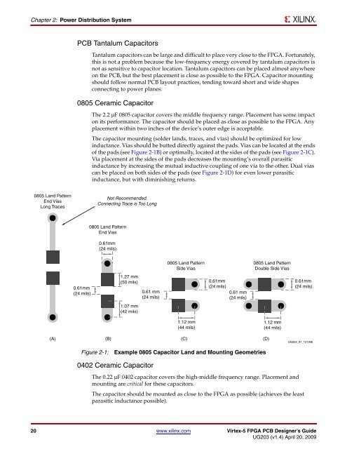
0805 Ceramic Capacitor<br />
0.61mm<br />
(24 mils)<br />
The 2.2 µF 0805 capacitor covers the middle frequency range. Placement has some impact<br />
on its performance. The capacitor should be placed as close as possible to the <strong>FPGA</strong>. Any<br />
placement within two inches of the device’s outer edge is acceptable.<br />
The capacitor mounting (solder lands, traces, and vias) should be optimized for low<br />
inductance. Vias should be butted directly against the pads. Vias can be located at the ends<br />
of the pads (see Figure 2-1B) or optimally, located at the sides of the pads (see Figure 2-1C).<br />
Via placement at the sides of the pads decreases the mounting’s overall parasitic<br />
inductance by increasing the mutual inductive coupling of one via to the other. Dual vias<br />
can be placed on both sides of the pads (see Figure 2-1D) for even lower parasitic<br />
inductance, but with diminishing returns.<br />
Not Recommended.<br />
Connecting Trace is Too Long<br />
0805 Land Pattern<br />
End Vias<br />
0.61mm<br />
(24 mils)<br />
(B)<br />
1.27 mm<br />
(50 mils)<br />
0.61 mm<br />
(24 mils)<br />
1.07 mm<br />
(42 mils)<br />
Figure 2-1: Example 0805 Capacitor Land and Mounting Geometries<br />
0402 Ceramic Capacitor<br />
0805 Land Pattern<br />
Side Vias<br />
1.12 mm<br />
(44 mils)<br />
<strong>UG203</strong>_01_121306<br />
The 0.22 µF 0402 capacitor covers the high-middle frequency range. Placement and<br />
mounting are critical for these capacitors.<br />
The capacitor should be mounted as close to the <strong>FPGA</strong> as possible (achieves the least<br />
parasitic inductance possible).<br />
20 www.xilinx.com <strong>Virtex</strong>-5 <strong>FPGA</strong> <strong>PCB</strong> Designer’s <strong>Guide</strong><br />
<strong>UG203</strong> (v1.4) April 20, 2009<br />
(C)<br />
0.61mm<br />
(24 mils)<br />
0.61 mm<br />
(24 mils)<br />
0805 Land Pattern<br />
Double Side Vias<br />
1.12 mm<br />
(44 mils)<br />
(D)<br />
0.61mm<br />
(24 mils)


