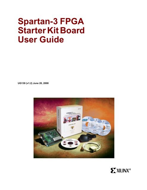
Xilinx UG130 Spartan-3 FPGA Starter Kit Board User Guide
Xilinx UG130 Spartan-3 FPGA Starter Kit Board User Guide
Xilinx UG130 Spartan-3 FPGA Starter Kit Board User Guide
You also want an ePaper? Increase the reach of your titles
YUMPU automatically turns print PDFs into web optimized ePapers that Google loves.
R<strong>Xilinx</strong> is disclosing this Document and Intellectual Property (hereinafter “the Design”) to you for use in the development of designs to operateon, or interface with <strong>Xilinx</strong> <strong>FPGA</strong>s. Except as stated herein, none of the Design may be copied, reproduced, distributed, republished,downloaded, displayed, posted, or transmitted in any form or by any means including, but not limited to, electronic, mechanical,photocopying, recording, or otherwise, without the prior written consent of <strong>Xilinx</strong>. Any unauthorized use of the Design may violate copyrightlaws, trademark laws, the laws of privacy and publicity, and communications regulations and statutes.<strong>Xilinx</strong> does not assume any liability arising out of the application or use of the Design; nor does <strong>Xilinx</strong> convey any license under its patents,copyrights, or any rights of others. You are responsible for obtaining any rights you may require for your use or implementation of theDesign. <strong>Xilinx</strong> reserves the right to make changes, at any time, to the Design as deemed desirable in the sole discretion of <strong>Xilinx</strong>. <strong>Xilinx</strong>assumes no obligation to correct any errors contained herein or to advise you of any correction if such be made. <strong>Xilinx</strong> will not assume anyliability for the accuracy or correctness of any engineering or technical support or assistance provided to you in connection with the Design.THE DESIGN IS PROVIDED “AS IS” WITH ALL FAULTS, AND THE ENTIRE RISK AS TO ITS FUNCTION AND IMPLEMENTATION ISWITH YOU. YOU ACKNOWLEDGE AND AGREE THAT YOU HAVE NOT RELIED ON ANY ORAL OR WRITTEN INFORMATION ORADVICE, WHETHER GIVEN BY XILINX, OR ITS AGENTS OR EMPLOYEES. XILINX MAKES NO OTHER WARRANTIES, WHETHEREXPRESS, IMPLIED, OR STATUTORY, REGARDING THE DESIGN, INCLUDING ANY WARRANTIES OF MERCHANTABILITY,FITNESS FOR A PARTICULAR PURPOSE, TITLE, AND NONINFRINGEMENT OF THIRD-PARTY RIGHTS.IN NO EVENT WILL XILINX BE LIABLE FOR ANY CONSEQUENTIAL, INDIRECT, EXEMPLARY, SPECIAL, OR INCIDENTALDAMAGES, INCLUDING ANY LOST DATA AND LOST PROFITS, ARISING FROM OR RELATING TO YOUR USE OF THE DESIGN,EVEN IF YOU HAVE BEEN ADVISED OF THE POSSIBILITY OF SUCH DAMAGES. THE TOTAL CUMULATIVE LIABILITY OF XILINX INCONNECTION WITH YOUR USE OF THE DESIGN, WHETHER IN CONTRACT OR TORT OR OTHERWISE, WILL IN NO EVENTEXCEED THE AMOUNT OF FEES PAID BY YOU TO XILINX HEREUNDER FOR USE OF THE DESIGN. YOU ACKNOWLEDGE THATTHE FEES, IF ANY, REFLECT THE ALLOCATION OF RISK SET FORTH IN THIS AGREEMENT cc THAT XILINX WOULD NOT MAKEAVAILABLE THE DESIGN TO YOU WITHOUT THESE LIMITATIONS OF LIABILITY.The Design is not designed or intended for use in the development of on-line control equipment in hazardous environments requiring failsafecontrols, such as in the operation of nuclear facilities, aircraft navigation or communications systems, air traffic control, life support, orweapons systems (“High-Risk Applications”). <strong>Xilinx</strong> specifically disclaims any express or implied warranties of fitness for such High-RiskApplications. You represent that use of the Design in such High-Risk Applications is fully at your risk.© 2004-2008 <strong>Xilinx</strong>, Inc. All rights reserved. XILINX, the <strong>Xilinx</strong> logo, and other designated brands included herein are trademarks of <strong>Xilinx</strong>,Inc. PowerPC is a trademark of IBM Corp. and used under license. PCI, PCI-X, and PCI EXPRESS are registered trademarks of PCI-SIG.All other trademarks are the property of their respective owners.Some portions reproduced by permission from Digilent, Inc.<strong>Spartan</strong>-3 <strong>FPGA</strong> <strong>Starter</strong> <strong>Kit</strong> <strong>Board</strong> <strong>User</strong> <strong>Guide</strong><strong>UG130</strong> (v1.2) June 20, 2008The following table shows the revision history for this document.VersionRevision04/26/04 1.0 Initial <strong>Xilinx</strong> release.06/07/04 1.0.1 Minor modifications for printed release.07/21/04 1.0.2 Added information on auxiliary serial port connections to Chapter 7.05/13/05 1.1 Clarified that SRAM IC10 shares eight lower data lines with A1 connector.06/20/08 1.2 Corrected A1 pins in Table 2-2. Updated links.<strong>Spartan</strong>-3 <strong>FPGA</strong> <strong>Starter</strong> <strong>Kit</strong> <strong>Board</strong> <strong>User</strong> <strong>Guide</strong> www.xilinx.com <strong>UG130</strong> (v1.2) June 20, 2008
RChapter 10: Platform Flash Configuration StoragePlatform Flash Jumper Options (JP1) . . . . . . . . . . . . . . . . . . . . . . . . . . . . . . . . . . . . . . . . 38“Default” Option . . . . . . . . . . . . . . . . . . . . . . . . . . . . . . . . . . . . . . . . . . . . . . . . . . . . . . . . . . . 38“Flash Read” Option . . . . . . . . . . . . . . . . . . . . . . . . . . . . . . . . . . . . . . . . . . . . . . . . . . . . . . . . 39“Disable” Option . . . . . . . . . . . . . . . . . . . . . . . . . . . . . . . . . . . . . . . . . . . . . . . . . . . . . . . . . . . 40Chapter 11: JTAG Programming/Debugging PortsJTAG Header (J7) . . . . . . . . . . . . . . . . . . . . . . . . . . . . . . . . . . . . . . . . . . . . . . . . . . . . . . . . . . . 41Parallel Cable IV/MultiPro Desktop Tool JTAG Header (J5). . . . . . . . . . . . . . . . . . 42Chapter 12: Power DistributionAC Wall Adapter. . . . . . . . . . . . . . . . . . . . . . . . . . . . . . . . . . . . . . . . . . . . . . . . . . . . . . . . . . . . 45Voltage Regulators . . . . . . . . . . . . . . . . . . . . . . . . . . . . . . . . . . . . . . . . . . . . . . . . . . . . . . . . . . 45Chapter 13: Expansion Connectors and <strong>Board</strong>sExpansion Connectors. . . . . . . . . . . . . . . . . . . . . . . . . . . . . . . . . . . . . . . . . . . . . . . . . . . . . . . 47A1 Connector Pinout . . . . . . . . . . . . . . . . . . . . . . . . . . . . . . . . . . . . . . . . . . . . . . . . . . . . . . 49A2 Connector Pinout . . . . . . . . . . . . . . . . . . . . . . . . . . . . . . . . . . . . . . . . . . . . . . . . . . . . . . 50B1 Connector Pinout . . . . . . . . . . . . . . . . . . . . . . . . . . . . . . . . . . . . . . . . . . . . . . . . . . . . . . 51Expansion <strong>Board</strong>s . . . . . . . . . . . . . . . . . . . . . . . . . . . . . . . . . . . . . . . . . . . . . . . . . . . . . . . . . . . 52Appendix A: <strong>Board</strong> SchematicsAppendix B: Reference Material for Major Components4 www.xilinx.com <strong>Spartan</strong>-3 <strong>FPGA</strong> <strong>Starter</strong> <strong>Kit</strong> <strong>Board</strong> <strong>User</strong> <strong>Guide</strong><strong>UG130</strong> (v1.2) June 20, 2008
RPrefaceAbout This <strong>Guide</strong><strong>Guide</strong> ContentsThis user guide describes the components and operation of the <strong>Spartan</strong> ® -3 <strong>FPGA</strong> <strong>Starter</strong><strong>Kit</strong> <strong>Board</strong>.This manual contains the following chapters:• Chapter 1, “Introduction”• Chapter 2, “Fast, Asynchronous SRAM”• Chapter 3, “Four-Digit, Seven-Segment LED Display”• Chapter 4, “Switches and LEDs”• Chapter 5, “VGA Port”• Chapter 6, “PS/2 Mouse/Keyboard Port”• Chapter 7, “RS-232 Serial Port”• Chapter 8, “Clock Sources”• Chapter 9, “<strong>FPGA</strong> Configuration Modes and Functions”• Chapter 10, “Platform Flash Configuration Storage”• Chapter 11, “JTAG Programming/Debugging Ports”• Chapter 12, “Power Distribution”• Chapter 13, “Expansion Connectors and <strong>Board</strong>s”• Appendix A, “<strong>Board</strong> Schematics”• Appendix B, “Reference Material for Major Components”<strong>Spartan</strong>-3 <strong>FPGA</strong> <strong>Starter</strong> <strong>Kit</strong> <strong>Board</strong> <strong>User</strong> <strong>Guide</strong> www.xilinx.com 5<strong>UG130</strong> (v1.2) June 20, 2008
RPreface: About This <strong>Guide</strong>6 www.xilinx.com <strong>Spartan</strong>-3 <strong>FPGA</strong> <strong>Starter</strong> <strong>Kit</strong> <strong>Board</strong> <strong>User</strong> <strong>Guide</strong><strong>UG130</strong> (v1.2) June 20, 2008
RChapter 1IntroductionThe <strong>Xilinx</strong> <strong>Spartan</strong> ® -3 <strong>FPGA</strong> <strong>Starter</strong> <strong>Kit</strong> provides a low-cost, easy-to-use development andevaluation platform for <strong>Spartan</strong>-3 <strong>FPGA</strong> designs.Key Components and FeaturesFigure 1-1 shows the <strong>Spartan</strong>-3 <strong>Starter</strong> <strong>Kit</strong> board, which includes the followingcomponents and features:• 200,000-gate <strong>Xilinx</strong> <strong>Spartan</strong>-3 XC3S200 <strong>FPGA</strong> in a 256-ball thin Ball Grid Arraypackage (XC3S200FT256) 1♦ 4,320 logic cell equivalents♦ Twelve 18K-bit block RAMs (216K bits)♦ Twelve 18x18 hardware multipliers♦ Four Digital Clock Managers (DCMs)♦ Up to 173 user-defined I/O signals• 2Mbit <strong>Xilinx</strong> XCF02S Platform Flash, in-system programmable configurationPROM 2♦ 1Mbit non-volatile data or application code storage available after <strong>FPGA</strong>configuration♦ Jumper options allow <strong>FPGA</strong> application to read PROM data or <strong>FPGA</strong>configuration from other sources 3• 1M-byte of Fast Asynchronous SRAM (bottom side of board, see Figure 1-3) 4♦ Two 256Kx16 ISSI IS61LV25616AL-10T 10 ns SRAMs♦ Configurable memory architecture- Single 256Kx32 SRAM array, ideal for MicroBlaze code images- Two independent 256Kx16 SRAM arrays♦ Individual chip select per device♦ Individual byte enables• 3-bit, 8-color VGA display port 5• 9-pin RS-232 Serial Port 6♦ DB9 9-pin female connector (DCE connector)♦ RS-232 transceiver/level translator 7♦ Uses straight-through serial cable to connect to computer or workstation serialport♦ Second RS-232 transmit and receive channel available on board test points 8<strong>Spartan</strong>-3 <strong>FPGA</strong> <strong>Starter</strong> <strong>Kit</strong> <strong>Board</strong> <strong>User</strong> <strong>Guide</strong> www.xilinx.com 7<strong>UG130</strong> (v1.2) June 20, 2008
RChapter 1: IntroductionDigilent Low-CostParallel Port to JTAGCable23IncludedParallel Cable IVMutliPro Desktop ToolJTAG Connector24Low-Cost JTAGDownload CableConnector222XCF02S 2MbitConfigurationPROMA1 ExpansionHeaderA2 ExpansionHeader21203Platform FlashOption JumpersB1 ExpansionHeader1945691011256Kx1610ns SRAM256Kx1610ns SRAM8-colorVGA PortRS-232 PortSerial PortPS/2 Port4 Character7-Segment LED8 Slide SwitchesRS-232Driver71XC3S200<strong>Spartan</strong>-3<strong>FPGA</strong>ConfigurationDONE LEDPROGRAMPush ButtonConfigurationMode SelectJumpersAuxiliaryOscillator Socket50 MHzOscillator4 Push Buttons8 LEDs18171615141312Power OnLED26VCCO3.3VRegulator2.5VRegulator1.2VRegulator27 28 295 VDC, 2A Supply100-240V AC Input50-60 Hz25AC Wall AdapterIncluded<strong>UG130</strong>_c1_01_042504Figure 1-1:<strong>Xilinx</strong> <strong>Spartan</strong>-3 <strong>Starter</strong> <strong>Kit</strong> <strong>Board</strong> Block Diagram• PS/2-style mouse/keyboard port• Four-character, seven-segment LED display• Eight slide switches• Eight individual LED outputs• Four momentary-contact push button switches1112910138 www.xilinx.com <strong>Spartan</strong>-3 <strong>FPGA</strong> <strong>Starter</strong> <strong>Kit</strong> <strong>Board</strong> <strong>User</strong> <strong>Guide</strong><strong>UG130</strong> (v1.2) June 20, 2008
Component LocationsRComponent Locations• 50 MHz crystal oscillator clock source (bottom side of board, see Figure 1-3)• Socket for an auxiliary crystal oscillator clock source• <strong>FPGA</strong> configuration mode selected via jumper settings• Push button switch to force <strong>FPGA</strong> reconfiguration (<strong>FPGA</strong> configuration happensautomatically at power-on) 17• LED indicates when <strong>FPGA</strong> is successfully configured 18• Three 40-pin expansion connection ports to extend and enhance the <strong>Spartan</strong>-3 <strong>Starter</strong><strong>Kit</strong> <strong>Board</strong> 19 20 21♦ See compatible expansion cards atwww.xilinx.com/products/boards/DO-SPAR3-DK/boards/daughtercards.htm♦ Compatible with Digilent, Inc. peripheral boardswww.digilentinc.com/Products/Catalog.cfm?Nav1=Products&Nav2=Peripheral&Cat=Peripheral♦ <strong>FPGA</strong> serial configuration interface signals available on the A2 and B1 connectors- PROG_B, DONE, INIT_B, CCLK, DONE• JTAG port 22 for low-cost download cable 23• Digilent JTAG download/debugging cable connects to PC parallel port 23• JTAG download/debug port compatible with the <strong>Xilinx</strong> Parallel Cable IV andMultiPRO Desktop Tool 24• AC power adapter input for included international unregulated +5V powersupply 25• Power-on indicator LED 26• On-board 3.3V 27 , 2.5V 28 , and 1.2V 29 regulatorsFigure 1-2 and Figure 1-3 indicate the component locations on the top side and bottom sideof the board, respectively.151614<strong>Spartan</strong>-3 <strong>FPGA</strong> <strong>Starter</strong> <strong>Kit</strong> <strong>Board</strong> <strong>User</strong> <strong>Guide</strong> www.xilinx.com 9<strong>UG130</strong> (v1.2) June 20, 2008
RChapter 1: Introduction21A1 Expansion Connector20A2 Expansion Connector5VGA3.3VPROG25POWER POWER2667RS-2328271718DONERS-23216123122152422MbitPlatformFlash11XILINXXC3S200<strong>FPGA</strong>1103B1 Expansion Connector30PS/291913ug130_c1_02_042704Figure 1-2:<strong>Xilinx</strong> <strong>Spartan</strong>-3 <strong>Starter</strong> <strong>Kit</strong> <strong>Board</strong> (Top Side)54256Kx16SRAM256Kx16SRAM2.5V282950MHz141.2V6Figure 1-3:<strong>Xilinx</strong> <strong>Spartan</strong>-3 <strong>Starter</strong> <strong>Kit</strong> <strong>Board</strong> (Bottom Side)ug130_c1_03_04270410 www.xilinx.com <strong>Spartan</strong>-3 <strong>FPGA</strong> <strong>Starter</strong> <strong>Kit</strong> <strong>Board</strong> <strong>User</strong> <strong>Guide</strong><strong>UG130</strong> (v1.2) June 20, 2008
RChapter 2Fast, Asynchronous SRAMThe <strong>Spartan</strong> ® -3 <strong>FPGA</strong> <strong>Starter</strong> <strong>Kit</strong> board has a megabyte of fast asynchronous SRAM,surface-mounted to the backside of the board. The memory array includes two 256Kx16ISSI IS61LV25616AL-10T 10 ns SRAM devices, as shown in Figure 2-1. A detailedschematic appears in Figure A-8.ISSI256Kx16 SRAM(10 ns)(see (see Table Table 2-3) 2-3)I/O[15:0]<strong>Spartan</strong>-3<strong>FPGA</strong>CE1UB1LB1(see (see Table 2-4)(P7)(T4)(P6)A[17:0]CEUBLBWEOEISSI256Kx16 SRAM(10 ns)I/O[15:0]IC10(see (see Table 2-1)A[17:0]CE2UB2LB2WEOE(N5)(R4)(P5)(G3)(K4)CEUBLBWEOEIC11(xx) = <strong>FPGA</strong> pin number<strong>UG130</strong>_c2_01_042604Figure 2-1:<strong>FPGA</strong> to SRAM Connections<strong>Spartan</strong>-3 <strong>FPGA</strong> <strong>Starter</strong> <strong>Kit</strong> <strong>Board</strong> <strong>User</strong> <strong>Guide</strong> www.xilinx.com 11<strong>UG130</strong> (v1.2) June 20, 2008
RChapter 2: Fast, Asynchronous SRAMAddress Bus ConnectionsThe SRAM array forms either a single 256Kx32 SRAM memory or two independent256Kx16 arrays. Both SRAM devices share common write-enable (WE#), output-enable(OE#), and address (A[17:0]) signals. However, each device has a separate chip selectenable (CE#) control and individual byte-enable controls to select the high or low byte inthe 16-bit data word, UB and LB, respectively.The 256Kx32 configuration is ideally suited to hold MicroBlaze instructions. However, italternately provides high-density data storage for a variety of applications, such as digitalsignal processing (DSP), large data FIFOs, and graphics buffers.Both 256Kx16 SRAMs share 18-bit address control lines, as shown in Table 2-1. Theseaddress signals also connect to the A1 Expansion Connector (see “Expansion Connectors,”page 47).Table 2-1: External SRAM Address Bus Connections to <strong>Spartan</strong>-3 <strong>FPGA</strong>Address Bit <strong>FPGA</strong> Pin A1 Expansion Connector PinA17 L3 35A16 K5 33A15 K3 34A14 J3 31A13 J4 32A12 H4 29A11 H3 30A10 G5 27A9 E4 28A8 E3 25A7 F4 26A6 F3 23A5 G4 24A4 L4 14A3 M3 12A2 M4 10A1 N3 8A0 L5 612 www.xilinx.com <strong>Spartan</strong>-3 <strong>FPGA</strong> <strong>Starter</strong> <strong>Kit</strong> <strong>Board</strong> <strong>User</strong> <strong>Guide</strong><strong>UG130</strong> (v1.2) June 20, 2008
Write Enable and Output Enable Control SignalsRWrite Enable and Output Enable Control SignalsBoth 256Kx16 SRAMs share common output enable (OE#) and write enable (WE#) controllines, as shown in Table 2-2. These control signals also connect to the A1 ExpansionConnector (refer to “Expansion Connectors,” page 47).Table 2-2:External SRAM Control Signal Connections to <strong>Spartan</strong>-3 <strong>FPGA</strong>Signal <strong>FPGA</strong> Pin A1 Expansion Connector PinOE# K4 18WE# G3 16SRAM Data Signals, Chip Enables, and Byte EnablesThe data signals, chip enables, and byte enables are dedicated connections between the<strong>FPGA</strong> and SRAM. Table 2-3 shows the <strong>FPGA</strong> pin connections to the SRAM designatedIC10 in Figure A-8. Table 2-4 shows the <strong>FPGA</strong> pin connections to SRAM IC11. To disable anSRAM, drive the associated chip enable pin High.Table 2-3: SRAM IC10 ConnectionsSignal <strong>FPGA</strong> Pin A1 Expansion Connector PinIO15R1IO14P1IO13L2IO12J2IO11H1IO10F2IO9P8IO8D3IO7 B1 19IO6 C1 17IO5 C2 15IO4 R5 13IO3 T5 11IO2 R6 9IO1 T8 7IO0 N7 5CE1 (chip enable IC10)P7UB1 (upper byte enable IC10) T4LB1 (lower byte enable IC10) P6<strong>Spartan</strong>-3 <strong>FPGA</strong> <strong>Starter</strong> <strong>Kit</strong> <strong>Board</strong> <strong>User</strong> <strong>Guide</strong> www.xilinx.com 13<strong>UG130</strong> (v1.2) June 20, 2008
RChapter 2: Fast, Asynchronous SRAMTable 2-4: SRAM IC11 ConnectionsSignal<strong>FPGA</strong> PinIO15N1IO14M1IO13K2IO12C3IO11F5IO10G1IO9E2IO8D2IO7D1IO6E1IO5G2IO4J1IO3K1IO2M2IO1N2IO0P2CE2 (chip enable IC11)N5UB2 (upper byte enable IC11) R4LB2 (lower byte enable IC11) P514 www.xilinx.com <strong>Spartan</strong>-3 <strong>FPGA</strong> <strong>Starter</strong> <strong>Kit</strong> <strong>Board</strong> <strong>User</strong> <strong>Guide</strong><strong>UG130</strong> (v1.2) June 20, 2008
RChapter 3Four-Digit, Seven-Segment LED DisplayThe <strong>Spartan</strong> ® -3 <strong>FPGA</strong> <strong>Starter</strong> <strong>Kit</strong> board has a four-character, seven segment LED displaycontrolled by <strong>FPGA</strong> user-I/O pins, as shown in Figure 3-1. Each digit shares eight commoncontrol signals to light individual LED segments. Each individual character has a separateanode control input. A detailed schematic for the display appears in Figure A-2.The pin number for each <strong>FPGA</strong> pin connected to the LED display appears in parentheses.To light an individual signal, drive the individual segment control signal Low along withthe associated anode control signal for the individual character. In Figure 3-1, for example,the left-most character displays the value ‘2’. The digital values driving the display in thisexample are shown in blue. The AN3 anode control signal is Low, enabling the controlinputs for the left-most character. The segment control inputs, A through G and DP, drivethe individual segments that comprise the character. A Low value lights the individualsegment, a High turns off the segment. A Low on the A input signal, lights segment ‘a’ ofthe display. The anode controls for the remaining characters, AN[2:0] are all High, andthese characters ignore the values presented on A through G and DP.AN3 (E13) AN2 (F14) AN1 (G14) AN0 (D14)01 1 1(E14)aaaa0A0B(F13)fb(G13)fbfbfb10CD(N16)gggg0E1F(R16)ec(N15)ececec0G1DPd(P15)dpddpddpddp(P16)<strong>UG130</strong>_c3_01_042704Figure 3-1:Seven-Segment LED Digit ControlTable 3-1 lists the <strong>FPGA</strong> connections that drive the individual LEDs comprising a sevensegmentcharacter. Table 3-2 lists the connections to enable a specific character. Table 3-3shows the patterns required to display hexadecimal characters.<strong>Spartan</strong>-3 <strong>FPGA</strong> <strong>Starter</strong> <strong>Kit</strong> <strong>Board</strong> <strong>User</strong> <strong>Guide</strong> www.xilinx.com 15<strong>UG130</strong> (v1.2) June 20, 2008
RChapter 3: Four-Digit, Seven-Segment LED DisplayTable 3-1:<strong>FPGA</strong> Connections to Seven-Segment Display (Active Low)Segment<strong>FPGA</strong> PinAE14BG13CN15DP15ER16FF13GN16DPP16Table 3-2: Digit Enable (Anode Control) Signals (Active Low)Anode Control AN3 AN2 AN1 AN0<strong>FPGA</strong> Pin E13 F14 G14 D14Table 3-3: Display Characters and Resulting LED Segment Control ValuesCharacter a b c d e f g0 0 0 0 0 0 0 11 1 0 0 1 1 1 12 0 0 1 0 0 1 03 0 0 0 0 1 1 04 1 0 0 1 1 0 05 0 1 0 0 1 0 06 0 1 0 0 0 0 07 0 0 0 1 1 1 18 0 0 0 0 0 0 09 0 0 0 0 1 0 0A 0 0 0 1 0 0 0b 1 1 0 0 0 0 0C 0 1 1 0 0 0 1d 1 0 0 0 0 1 0E 0 1 1 0 0 0 0F 0 1 1 1 0 0 016 www.xilinx.com <strong>Spartan</strong>-3 <strong>FPGA</strong> <strong>Starter</strong> <strong>Kit</strong> <strong>Board</strong> <strong>User</strong> <strong>Guide</strong><strong>UG130</strong> (v1.2) June 20, 2008
RThe LED control signals are time-multiplexed to display data on all four characters, asshown in Figure 3-2. Present the value to be displayed on the segment control inputs andselect the specified character by driving the associated anode control signal Low. Throughpersistence of vision, the human brain perceives that all four characters appearsimultaneously, similar to the way the brain perceives a TV display.AN3AN2AN1AN0{A,B,C,D,E,F,G,DP}DISP3 DISP2 DISP1 DISP0<strong>UG130</strong>_c3_02_042404Figure 3-2:Drive Anode Input Low to Light an Individual CharacterThis “scanning” technique reduces the number of I/O pins required for the fourcharacters. If an <strong>FPGA</strong> pin were dedicated for each individual segment, then 32 pins arerequired to drive four 7-segment LED characters. The scanning technique reduces therequired I/O down to 12 pins. The drawback to this approach is that the <strong>FPGA</strong> logic mustcontinuously scan data out to the displays—a small price to save 20 additional I/O pins.<strong>Spartan</strong>-3 <strong>FPGA</strong> <strong>Starter</strong> <strong>Kit</strong> <strong>Board</strong> <strong>User</strong> <strong>Guide</strong> www.xilinx.com 17<strong>UG130</strong> (v1.2) June 20, 2008
RChapter 3: Four-Digit, Seven-Segment LED Display18 www.xilinx.com <strong>Spartan</strong>-3 <strong>FPGA</strong> <strong>Starter</strong> <strong>Kit</strong> <strong>Board</strong> <strong>User</strong> <strong>Guide</strong><strong>UG130</strong> (v1.2) June 20, 2008
RChapter 4Switches and LEDsSlide SwitchesThe <strong>Spartan</strong> ® -3 <strong>FPGA</strong> <strong>Starter</strong> <strong>Kit</strong> board has eight slide switches, indicated as 11 inFigure 1-2. The switches are located along the lower edge of the board, toward the rightedge. The switches are labeled SW7 through SW0. Switch SW7 is the left-most switch, andSW0 is the right-most switch. The switches connect to an associated <strong>FPGA</strong> pin, as shown inTable 4-1. A detailed schematic appears in Figure A-2.Table 4-1:Push Button SwitchesSlider Switch ConnectionsSwitch SW7 SW6 SW5 SW4 SW3 SW2 SW1 SW0<strong>FPGA</strong> Pin K13 K14 J13 J14 H13 H14 G12 F12When in the UP or ON position, a switch connects the <strong>FPGA</strong> pin to V CCO , a logic High.When DOWN or in the OFF position, the switch connects the <strong>FPGA</strong> pin to ground, a logicLow. The switches typically exhibit about 2 ms of mechanical bounce and there is no activedebouncing circuitry, although such circuitry could easily be added to the <strong>FPGA</strong> designprogrammed on the board. A 4.7KΩ series resistor provides nominal input protection.The <strong>Spartan</strong>-3 <strong>Starter</strong> <strong>Kit</strong> board has four momentary-contact push button switches,indicated as 13 in Figure 1-2. These push buttons are located along the lower edge of theboard, toward the right edge. The switches are labeled BTN3 through BTN0. Push buttonswitch BTN3 is the left-most switch, BTN0 the right-most switch. The push buttonswitches connect to an associated <strong>FPGA</strong> pin, as shown in Table 4-2. A detailed schematicappears in Figure A-2.Table 4-2:Push Button Switch ConnectionsPush Button BTN3 (<strong>User</strong> Reset) BTN2 BTN1 BTN0<strong>FPGA</strong> Pin L14 L13 M14 M13Pressing a push button generates a logic High on the associated <strong>FPGA</strong> pin. Again, there isno active debouncing circuitry on the push button.The left-most button, BTN3, is also the default <strong>User</strong> Reset pin. BTN3 electrically behavesidentically to the other push buttons. However, when applicable, BTN3 resets theprovided reference designs.<strong>Spartan</strong>-3 <strong>FPGA</strong> <strong>Starter</strong> <strong>Kit</strong> <strong>Board</strong> <strong>User</strong> <strong>Guide</strong> www.xilinx.com 19<strong>UG130</strong> (v1.2) June 20, 2008
RChapter 5VGA PortThe <strong>Spartan</strong> ® -3 <strong>FPGA</strong> <strong>Starter</strong> <strong>Kit</strong> board includes a VGA display port and DB15 connector,indicated as 5 in Figure 1-2. Connect this port directly to most PC monitors or flat-panelLCD displays using a standard monitor cable.Pin 5Pin 10Pin 1Pin 6Pin 15Pin 1112345DB15Connector6117128139141015RedGreenBlueHorizontal SyncVertical SyncDB15 VGA Connector(front view)270Ω270Ω270ΩRGBHSVS(R12)(T12)(R11)(R9)(T10)(xx) = <strong>FPGA</strong> pin numberGND<strong>UG130</strong>_c5_01_042604Figure 5-1:VGA Connections from <strong>Spartan</strong>-3 <strong>Starter</strong> <strong>Kit</strong> <strong>Board</strong>As shown in Figure 5-1, the <strong>Spartan</strong>-3 <strong>FPGA</strong> controls five VGA signals: Red (R), Green (G),Blue (B), Horizontal Sync (HS), and Vertical Sync (VS), all available on the VGA connector.The <strong>FPGA</strong> pins that drive the VGA port appear in Table 5-1. A detailed schematic is inFigure A-7.<strong>Spartan</strong>-3 <strong>FPGA</strong> <strong>Starter</strong> <strong>Kit</strong> <strong>Board</strong> <strong>User</strong> <strong>Guide</strong> www.xilinx.com 21<strong>UG130</strong> (v1.2) June 20, 2008
RChapter 5: VGA PortTable 5-1:Red (R)Green (G)Blue (B)VGA Port Connections to the <strong>Spartan</strong>-3 <strong>FPGA</strong>SignalHorizontal Sync (HS)Vertical Sync (VS)<strong>FPGA</strong> PinEach color line has a series resistor to provide 3-bit color, with one bit each for Red, Green,and Blue. The series resistor uses the 75Ω VGA cable termination to ensure that the colorsignals remain in the VGA-specified 0V to 0.7V range. The HS and VS signals are TTL level.Drive the R, G, and B signals High or Low to generate the eight possible colors shown inTable 5-2.R12T12R11R9T10Table 5-2:3-Bit Display Color CodesRed (R) Green (G) Blue (B) Resulting Color0 0 0 Black0 0 1 Blue0 1 0 Green0 1 1 Cyan1 0 0 Red1 0 1 Magenta1 1 0 Yellow1 1 1 WhiteVGA signal timing is specified, published, copyrighted, and sold by the Video ElectronicsStandards Association (VESA). The following VGA system and timing information isprovided as an example of how the <strong>FPGA</strong> might drive VGA monitor in 640 by 480 mode.For more precise information or for information on higher VGA frequencies, refer todocuments available on the VESA website or other electronics websites:• Video Electronics Standards Associationhttp://www.vesa.org• VGA Timing Informationhttp://www.epanorama.net/documents/pc/vga_timing.htmlSignal Timing for a 60Hz, 640x480 VGA DisplayCRT-based VGA displays use amplitude-modulated, moving electron beams (or cathoderays) to display information on a phosphor-coated screen. LCD displays use an array ofswitches that can impose a voltage across a small amount of liquid crystal, therebychanging light permitivity through the crystal on a pixel-by-pixel basis. Although thefollowing description is limited to CRT displays, LCD displays have evolved to use the22 www.xilinx.com <strong>Spartan</strong>-3 <strong>FPGA</strong> <strong>Starter</strong> <strong>Kit</strong> <strong>Board</strong> <strong>User</strong> <strong>Guide</strong><strong>UG130</strong> (v1.2) June 20, 2008
Signal Timing for a 60Hz, 640x480 VGA DisplayRsame signal timings as CRT displays. Consequently, the following discussion pertains toboth CRTs and LCD displays.Within a CRT display, current waveforms pass through the coils to produce magneticfields that deflect electron beams to transverse the display surface in a “raster” pattern,horizontally from left to right and vertically from top to bottom. As shown in Figure 5-2,information is only displayed when the beam is moving in the “forward” direction—left toright and top to bottom—and not during the time the beam returns back to the left or topedge of the display. Much of the potential display time is therefore lost in “blanking”periods when the beam is reset and stabilized to begin a new horizontal or vertical displaypass.pixel 0,0pixel 0,639640 pixels are displayed eachtime the beam traverses the screenCurrentthrough thehorizontaldeflectioncoilVGA Displaypixel 479,0 pixel 479,639Stable current ramp: Information isdisplayed during this timeRetrace: Noinformationis displayedduringthis timetimeTotal horizontal timeHorizontal display timeretrace time"back porch""back porch"HSHorizontal sync signalsets the retrace frequency"front porch"<strong>UG130</strong>_c5_02_051305Figure 5-2:CRT Display Timing ExampleThe size of the beams, the frequency at which the beam traces across the display, and thefrequency at which the electron beam is modulated determine the display resolution.<strong>Spartan</strong>-3 <strong>FPGA</strong> <strong>Starter</strong> <strong>Kit</strong> <strong>Board</strong> <strong>User</strong> <strong>Guide</strong> www.xilinx.com 23<strong>UG130</strong> (v1.2) June 20, 2008
RChapter 5: VGA PortVGA Signal TimingModern VGA displays support multiple display resolutions, and the VGA controllerdictates the resolution by producing timing signals to control the raster patterns. Thecontroller produces TTL-level synchronizing pulses that set the frequency at which currentflows through the deflection coils, and it ensures that pixel or video data is applied to theelectron guns at the correct time.Video data typically comes from a video refresh memory with one or more bytes assignedto each pixel location. The <strong>Spartan</strong>-3 <strong>Starter</strong> <strong>Kit</strong> board uses three bits per pixel, producingone of the eight possible colors shown in Table 5-2. The controller indexes into the videodata buffer as the beams move across the display. The controller then retrieves and appliesvideo data to the display at precisely the time the electron beam is moving across a givenpixel.As shown in Figure 5-2, the VGA controller generates the HS (horizontal sync) and VS(vertical sync) timings signals and coordinates the delivery of video data on each pixelclock. The pixel clock defines the time available to display one pixel of information. The VSsignal defines the “refresh” frequency of the display, or the frequency at which allinformation on the display is redrawn. The minimum refresh frequency is a function of thedisplay’s phosphor and electron beam intensity, with practical refresh frequencies in the60 Hz to 120 Hz range. The number of horizontal lines displayed at a given refreshfrequency defines the horizontal “retrace” frequency.The signal timings in Table 5-3 are derived for a 640-pixel by 480-row display using a25 MHz pixel clock and 60 Hz ±1 refresh. Figure 5-3 shows the relation between each of thetiming symbols. The timing for the sync pulse width (T PW ) and front and back porchintervals (T FP and T BP ) are based on observations from various VGA displays. The frontand back porch intervals are the pre- and post-sync pulse times. Information cannot bedisplayed during these times.Table 5-3: 640x480 Mode VGA TimingSymbol ParameterVertical SyncHorizontal SyncTime Clocks Lines Time ClocksT S Sync pulse time 16.7 ms 416,800 521 32 μs 800T DISP Display time 15.36 ms 384,000 480 25.6 μs 640T PW Pulse width 64 μs 1,600 2 3.84 μs 96T FP Front porch 320 μs 8,000 10 640 ns 16T BP Back porch 928 μs 23,200 29 1.92 μs 48T ST DISPT FPT PWT BPFigure 5-3:VGA Control Timing<strong>UG130</strong>_c5_03_05130524 www.xilinx.com <strong>Spartan</strong>-3 <strong>FPGA</strong> <strong>Starter</strong> <strong>Kit</strong> <strong>Board</strong> <strong>User</strong> <strong>Guide</strong><strong>UG130</strong> (v1.2) June 20, 2008
RChapter 5: VGA Port26 www.xilinx.com <strong>Spartan</strong>-3 <strong>FPGA</strong> <strong>Starter</strong> <strong>Kit</strong> <strong>Board</strong> <strong>User</strong> <strong>Guide</strong><strong>UG130</strong> (v1.2) June 20, 2008
RChapter 6: PS/2 Mouse/Keyboard Portbidirectional keyboard communications. As shown in Figure 6-2, the attached keyboard ormouse writes a bit on the data line when the clock signal is High, and the host reads thedata line when the clock signal is Low.Table 6-2: PS/2 Bus TimingSymbol Parameter Min MaxT CK Clock High or Low time 30 μs 50 μsT SU Data-to-clock setup time 5 μs 25 μsT HLD Clock-to-data hold time 5 μs 25 μsCLK (PS2C)DATA (PS2D)T CKT CKEdge 0 Edge 10T HLDT SU'0' start bit'1' stop bit<strong>UG130</strong>_c6_02_042404Figure 6-2:PS/2 Bus Timing WaveformsThe following site contains additional information on the PS/2 bus protocol:• PS/2 Mouse/Keyboard Protocolhttp://www.computer-engineering.org/ps2protocol/KeyboardThe keyboard uses open-collector drivers so that either the keyboard or the host can drivethe two-wire bus. If the host never sends data to the keyboard, then the host can use simpleinput pins.A PS/2-style keyboard uses scan codes to communicate key press data. Nearly allkeyboards in use today are PS/2 style. Each key has a single, unique scan code that is sentwhenever the corresponding key is pressed. The scan codes for most keys appear inFigure 6-3.If the key is pressed and held, the keyboard repeatedly sends the scan code every 100 ms orso. When a key is released, the keyboard sends a “F0” key-up code, followed by the scancode of the released key. The keyboard sends the same scan code, regardless if a key hasdifferent “shift” and “non-shift” characters and regardless whether the Shift key is pressedor not. The host determines which character is intended.Some keys, called extended keys, send an “E0” ahead of the scan code and furthermore,they may send more than one scan code. When an extended key is released, a “E0 F0” keyupcode is sent, followed by the scan code.28 www.xilinx.com <strong>Spartan</strong>-3 <strong>FPGA</strong> <strong>Starter</strong> <strong>Kit</strong> <strong>Board</strong> <strong>User</strong> <strong>Guide</strong><strong>UG130</strong> (v1.2) June 20, 2008
KeyboardRESC76F105F206F304F40CF503F60BF783F80AF901F1009F1178F1207 E0 75` ~0ETAB0DCaps Lock58Shift12Ctrl141 !16Q152 @1EW1DA1CZ1Z3 #26S1BAlt11E24X224 $25D23R2DC215 %2EF2BT2CV2A6 ^36Y35G34B327 &3DH33U3CN31Space298 *3EJ3BM3AI439 (46K42O44, .49- _4E; :4C/ ?4A[ {54AltE0 11= +55' "52] }5BBack Space66\ |5DEnter5AShift59CtrlE0 14E0 74E0 6BE0 72<strong>UG130</strong>_c6_03_042404Figure 6-3:PS/2 Keyboard Scan CodesTable 6-3:CommandEDThe host can also send data to the keyboard. Table 6-3 provides a short list of some oftenusedcommands.Common PS/2 Keyboard CommandsDescriptionTurn on/off Num Lock, Caps Lock, and Scroll Lock LEDs. The keyboard acknowledges receipt ofan “ED” command by replying with an “FA”, after which the host sends another byte to set LEDstatus. The bit positions for the keyboard LEDs appear in Table 6-4. Write a ‘1’ to the specific bit toilluminate the associated keyboard LED.Table 6-4:Keyboard LED Control7 6 5 4 3 2 1 0IgnoredCapsLockNumLockScrollLockEEF3FEFFEcho. Upon receiving an echo command, the keyboard replies with the same scan code “EE”.Set scan code repeat rate. The keyboard acknowledges receipt of an “F3” by returning an “FA”,after which the host sends a second byte to set the repeat rate.Resend. Upon receiving a resend command, the keyboard resends the last scan code sent.Reset. Resets the keyboard.The keyboard sends data to the host only when both the data and clock lines are High, theIdle state.Because the host is the “bus master”, the keyboard checks whether the host is sending databefore driving the bus. The clock line can be used as a “clear to send” signal. If the hostpulls the clock line Low, the keyboard must not send any data until the clock is released.The keyboard sends data to the host in 11-bit words that contain a ‘0’ start bit, followed byeight bits of scan code (LSB first), followed by an odd parity bit and terminated with a ‘1’stop bit. When the keyboard sends data, it generates 11 clock transitions at around 20 to30 kHz, and data is valid on the falling edge of the clock as shown in Figure 6-2.<strong>Spartan</strong>-3 <strong>FPGA</strong> <strong>Starter</strong> <strong>Kit</strong> <strong>Board</strong> <strong>User</strong> <strong>Guide</strong> www.xilinx.com 29<strong>UG130</strong> (v1.2) June 20, 2008
RChapter 6: PS/2 Mouse/Keyboard PortThe following site contains more information on PS/2 keyboard interfaces:• The PS/2 Keyboard Interfacehttp://www.computer-engineering.org/index.php?title=PS/2_Keyboard_InterfaceMouseA mouse generates a clock and data signal when moved; otherwise, these signals remainHigh indicating the Idle state. Each time the mouse is moved, the mouse sends three 11-bitwords to the host. Each of the 11-bit words contains a ‘0’ start bit, followed by 8 data bits(LSB first), followed by an odd parity bit, and terminated with a ‘1’ stop bit. Each datatransmission contains 33 total bits, where bits 0, 11, and 22 are ‘0’ start bits, and bits 10, 21,and 32 are ‘1’ stop bits. The three 8-bit data fields contain movement data as shown inFigure 6-4. Data is valid at the falling edge of the clock, and the clock period is 20 to 30 kHz.Mouse status byte X direction byte Y direction byte10 L R 0 1 XS YS XV YV P 1 0 X0 X1 X2 X3 X4 X5 X6 X7 P 1 0 Y0 Y1 Y2 Y3 Y4 Y5 Y6 Y7 P 1Idle stateStart bitStop bit Stop bit Stop bitStart bitStart bitIdle state<strong>UG130</strong>_c6_04_042404Figure 6-4:PS/2 Mouse TransactionAs shown in Figure 6-5, a PS/2 mouse employs a relative coordinate system whereinmoving the mouse to the right generates a positive value in the X field, and moving to theleft generates a negative value. Likewise, moving the mouse up generates a positive valuein the Y field, and moving down represents a negative value. The XS and YS bits in thestatus byte define the sign of each value, where a ‘1’ indicates a negative value.+Y values (YS=0)-X values(XS=1)+X values(XS=0)-Y values (YS=1)<strong>UG130</strong>_c6_05_042404Figure 6-5:The Mouse Uses a Relative Coordinate System to Track MovementThe magnitude of the X and Y values represent the rate of mouse movement. The larger thevalue, the faster the mouse is moving. The XV and YV bits in the status byte indicate whenthe X or Y values exceed their maximum value, an overflow condition. A ‘1’ indicates when30 www.xilinx.com <strong>Spartan</strong>-3 <strong>FPGA</strong> <strong>Starter</strong> <strong>Kit</strong> <strong>Board</strong> <strong>User</strong> <strong>Guide</strong><strong>UG130</strong> (v1.2) June 20, 2008
Voltage SupplyRVoltage Supplyan overflow occurs. If the mouse moves continuously, the 33-bit transmissions repeatevery 50 ms or so.The L and R fields in the status byte indicate Left and Right button presses. A ‘1’ indicatesthat the associated mouse button is being pressed.The following site contains additional information on interfacing to a PS/2-style mouse:• The PS/2 Mouse Interfacehttp://www.computer-engineering.org/index.php?title=PS/2_Mouse_InterfaceMost modern keyboards and mice work equally well from a 3.3V or 5V supply. The voltagesupply for the PS/2 port is selectable via the JP2 jumper, indicated as 30 in Figure 1-2,located immediately above the PS/2 connector along the right edge. The 3.3V setting ispreferred as the <strong>FPGA</strong>’s output signals operate from the 3.3V supply. The JP2 jumpershould be positioned as shown in Table 6-5 by default.Table 6-5:PS/2 Port Supply Voltage OptionsPS/2 PortSupply Voltage3.3V(DEFAULT)5VJumper JP2Setting3.3V3.3VJP2JP2VUVUSome older keyboards and mice are 5V only. Consequently, the JP2 jumper should be setfor 5V operation as shown in Table 6-5. The <strong>Spartan</strong>-3 <strong>FPGA</strong> can tolerate 5V signals due tothe 270Ω series resistors on the PS/2 data and clock signals connected to the <strong>FPGA</strong>. See theschematic in Figure A-7 for more details.<strong>Spartan</strong>-3 <strong>FPGA</strong> <strong>Starter</strong> <strong>Kit</strong> <strong>Board</strong> <strong>User</strong> <strong>Guide</strong> www.xilinx.com 31<strong>UG130</strong> (v1.2) June 20, 2008
RChapter 6: PS/2 Mouse/Keyboard Port32 www.xilinx.com <strong>Spartan</strong>-3 <strong>FPGA</strong> <strong>Starter</strong> <strong>Kit</strong> <strong>Board</strong> <strong>User</strong> <strong>Guide</strong><strong>UG130</strong> (v1.2) June 20, 2008
RChapter 7RS-232 Serial PortThe <strong>Spartan</strong> ® -3 <strong>FPGA</strong> <strong>Starter</strong> <strong>Kit</strong> board has an RS-232 serial port. The RS-232 transmit andreceive signals appear on the female DB9 connector, labeled J2, indicated as 6 inFigure 1-2. The connector is a DCE-style port and connects to the DB9 DTE-style serial portconnector available on most personal computers and workstations. Use a standardstraight-through serial cable to connect the <strong>Spartan</strong>-3 <strong>Starter</strong> <strong>Kit</strong> board to the PC’s serialport.Pin 5Pin 16DB9Connector123456789GNDMaxim MAX3232RS232 VoltageTranslator7DOUT1RIN1DOUT2RIN2DIN1ROUT1DIN2ROUT2Pin 9TXDRXDTXD-ARXD-ADB9 Serial Port Connector(front view)1R13T13T14N10Pin 6<strong>Spartan</strong>-3 <strong>FPGA</strong>8ReceiverTransmitterJ1 HeaderAuxiliary Serial PortLD7 LD6 LD5<strong>FPGA</strong> pin number<strong>UG130</strong>_c7_01_072104Figure 7-1:RS-232 Serial PortFigure 7-1 shows the connection between the <strong>FPGA</strong> and the DB9 connector, including theMaxim MAX3232 RS-232 voltage converter, indicated as 7 in Figure 1-2. The <strong>FPGA</strong>supplies serial output data as LVTTL or LVCMOS levels to the Maxim device, which in<strong>Spartan</strong>-3 <strong>FPGA</strong> <strong>Starter</strong> <strong>Kit</strong> <strong>Board</strong> <strong>User</strong> <strong>Guide</strong> www.xilinx.com 33<strong>UG130</strong> (v1.2) June 20, 2008
RChapter 7: RS-232 Serial Portturn, converts the logic value to the appropriate RS-232 voltage level. Likewise, the Maximdevice converts the RS-232 serial input data to LVTTL levels for the <strong>FPGA</strong>. A series resistorbetween the Maxim output pin and the <strong>FPGA</strong>’s RXD pin protects against accidental logicconflicts. A detailed schematic appears in Figure A-7.Hardware flow control is not supported on the connector. The port’s DCD, DTR, and DSRsignals connect together, as shown in Figure 7-1. Similarly, the port’s RTS and CTS signalsconnect together.The <strong>FPGA</strong> connections to the Maxim RS-232 translator appear in Table 7-1.Table 7-1:SignalRXDTXDRXD-ATXD-AAccessory Port Connections to the <strong>Spartan</strong>-3 <strong>FPGA</strong><strong>FPGA</strong> PinT13R13N10T14An auxiliary RS-232 serial channel from the Maxim device is available on two 0.1-inchstake pins, indicated as J1 in the schematic and 8 in Figure 1-2. The J1 stake pins are inthe lower left corner of the board, to the right of the DB9 serial connector, below the MaximRS-232 voltage translator, and to the left of the individual LEDs. The transmitter outputfrom the Maxim device drives the bottom stake pin while the receiver input connects to thetop stake pin.The <strong>FPGA</strong> auxiliary RS-232 connections to the Maxim device appear in Table 7-1 withsignals RXD-A and TXD-A. Ignore the pin numbers listed on the silkscreen markings nextto the stake pins as these apply to the connections to the DB9 connector.Place a jumper across the stake pins for an easy loop-back test. Alternately, create customserial ports by attaching the stake pins to other types of serial connectors such as male orfemale DB9 or DB25 cable connectors or even create null modem connections.34 www.xilinx.com <strong>Spartan</strong>-3 <strong>FPGA</strong> <strong>Starter</strong> <strong>Kit</strong> <strong>Board</strong> <strong>User</strong> <strong>Guide</strong><strong>UG130</strong> (v1.2) June 20, 2008
RChapter 8Clock SourcesThe <strong>Spartan</strong> ® -3 <strong>FPGA</strong> <strong>Starter</strong> <strong>Kit</strong> board has a dedicated 50 MHz Epson SG-8002JF seriesclock oscillator source and an optional socket for another clock oscillator source.Figure A-5 provides a detailed schematic for the clock sources.The 50 MHz clock oscillator is mounted on the bottom side of the board, indicated as 14in Figure A-5. Use the 50 MHz clock frequency as is or derive other frequencies using the<strong>FPGA</strong>s Digital Clock Managers (DCMs).• Chapter 3: Using Digital Clock Managers (DCMs) in <strong>Spartan</strong>-3 <strong>FPGA</strong>swww.xilinx.com/support/documentation/user_guides/ug331.pdfThe oscillator socket, indicated asfootprint.15in Figure 1-2, accepts oscillators in an 8-pin DIPTable 8-1:Clock Oscillator SourcesOscillator Source<strong>FPGA</strong> Pin50 MHz (IC4) T9Socket (IC8)D9<strong>Spartan</strong>-3 <strong>FPGA</strong> <strong>Starter</strong> <strong>Kit</strong> <strong>Board</strong> <strong>User</strong> <strong>Guide</strong> www.xilinx.com 35<strong>UG130</strong> (v1.2) June 20, 2008
RChapter 9<strong>FPGA</strong> Configuration Modes andFunctions<strong>FPGA</strong> Configuration Mode SettingsIn most applications for the <strong>Spartan</strong> ® -3 <strong>FPGA</strong> <strong>Starter</strong> <strong>Kit</strong> <strong>Board</strong>, the <strong>FPGA</strong> automaticallyboots from the on-board Platform Flash memory whenever power is applied or the PROGpush button is pressed. However, the board supports all the available configuration modesvia the J8 header, indicated as 16 in Figure 1-2. Table 9-1 provides the available optionsettings for the J8 header. Additionally, the JP1 jumper setting is required when usingMaster Serial configuration mode, as further described in “Platform Flash Jumper Options(JP1).”The default jumper settings for the board are:• All jumpers in the J8 header are installed• The JP1 jumper is in the “Default” positionTable 9-1: Header J8 Controls the <strong>FPGA</strong> Configuration ModeConfigurationHeader J8 Jumper JP1ModeSettings SettingMaster SerialGNDM0 M1 M2J8MODEorJP1JP1DescriptionDEFAULT. The <strong>FPGA</strong> automatically boots from the PlatformFlash.JP1The <strong>FPGA</strong> attempts to boot from a serial configuration sourceattached to either expansion connector A2 or B1.Slave SerialGNDM0 M1 M2J8MODEJP1Another device connected to either the A2 or B1 expansionconnector provides serial data and clock to load the <strong>FPGA</strong>.Master ParallelGNDM0 M1 M2J8MODEJP1The <strong>FPGA</strong> attempts to boot from a parallel configuration sourceattached to the B1 expansion connector.<strong>Spartan</strong>-3 <strong>FPGA</strong> <strong>Starter</strong> <strong>Kit</strong> <strong>Board</strong> <strong>User</strong> <strong>Guide</strong> www.xilinx.com 36<strong>UG130</strong> (v1.2) June 20, 2008
Program Push Button/DONE Indicator LEDRTable 9-1:ConfigurationModeSlave ParallelHeader J8 Controls the <strong>FPGA</strong> Configuration Mode (Continued)Header J8SettingsGNDM0 M1 M2J8MODEJumper JP1SettingJP1DescriptionAnother device connected to the B1 expansion connectorprovides parallel data and clock to load the <strong>FPGA</strong>.JTAGGNDM0 M1 M2J8MODEJP1The <strong>FPGA</strong> waits for configuration via the four-wire JTAGinterface.Program Push Button/DONE Indicator LEDThe <strong>Spartan</strong>-3 <strong>Starter</strong> <strong>Kit</strong> <strong>Board</strong> includes two <strong>FPGA</strong> configuration functions, located nearthe VGA connector and the AC power input connector, as shown in Figure 9-1. The PROGpush button, shown as 17 in Figure 9-1, drives the <strong>FPGA</strong>’s PROG_B programming pin.When pressed, the PROG push button forces the <strong>FPGA</strong> to reconfigure and reload itconfiguration data.The DONE LED, shown as 18 in Figure 9-1, connects to the <strong>FPGA</strong>’s DONE pin and lightsup when the <strong>FPGA</strong> is successfully configured.VGAVGA1718DONEPROG<strong>UG130</strong>_c9_03_042704Figure 9-1:The PROG Button and the DONE LED<strong>Spartan</strong>-3 <strong>FPGA</strong> <strong>Starter</strong> <strong>Kit</strong> <strong>Board</strong> <strong>User</strong> <strong>Guide</strong> www.xilinx.com 37<strong>UG130</strong> (v1.2) June 20, 2008
RChapter 10Platform Flash Configuration StorageThe <strong>Spartan</strong> ® -3 <strong>FPGA</strong> <strong>Starter</strong> <strong>Kit</strong> board has an XCF02S serial configuration Flash PROM tostore <strong>FPGA</strong> configuration data and potentially additional non-volatile data, includingMicroBlaze application code. To configure the <strong>FPGA</strong> from Platform Flash memory, allthree jumpers must be installed on the J8 header, indicated as 16 in Figure 1-2.Platform Flash Jumper Options (JP1)The Platform Flash has three optional settings controlled by the JP1 jumper, which islocated in the upper right-hand corner of the board, adjacent to the Platform Flashconfiguration PROM. The JP1 jumper is indicated as 3 in Figure 1-2. A detailedschematic is provided in Figure A-4. Table 10-1 summarizes the available options, whichare described in more detail below.Table 10-1:OptionDefaultJumper JP1 Controls the Platform Flash OptionsJumper JP1SettingJP1DescriptionThe <strong>FPGA</strong> boots from Platform Flash. No additional data storage is available.Flash ReadDisableJP1JP1The <strong>FPGA</strong> boots from Platform Flash, which is permanently enabled. The <strong>FPGA</strong>can read additional data from Platform Flash.Jumper removed. Platform Flash is disabled. Other configuration data sourceprovides <strong>FPGA</strong> boot data.“Default” OptionFor most applications, this is the default jumper setting. As shown in Figure 10-1, thePlatform Flash is enabled only during configuration when the <strong>FPGA</strong>’s DONE pin is Low.When the DONE pin goes High at the end of configuration, the Platform Flash is disabledand placed in low-power mode.<strong>Spartan</strong>-3 <strong>FPGA</strong> <strong>Starter</strong> <strong>Kit</strong> <strong>Board</strong> <strong>User</strong> <strong>Guide</strong> www.xilinx.com 38<strong>UG130</strong> (v1.2) June 20, 2008
“Flash Read” OptionR<strong>Spartan</strong>-3 <strong>FPGA</strong>M0 DIN/D0M1 INIT_BPlatform FlashD0OE/RESETDefaultJP1J8MODEM2DONECCLKCECLKUSER I/ORCLK<strong>UG130</strong>_c10_01_060704Figure 10-1:Default Platform Flash Option“Flash Read” OptionThe <strong>Spartan</strong>-3 <strong>Starter</strong> <strong>Kit</strong> <strong>Board</strong> includes a 2Mbit Platform Flash configuration PROM. TheXC3S200 <strong>FPGA</strong> on the board only requires slightly less than 1Mbit for configuration data.The remainder of the Platform Flash is available to store other non-volatile data, such asrevision codes, serial numbers, coefficients, an Ethernet MAC ID, or code for an embeddedprocessor, such as MicroBlaze, within the <strong>FPGA</strong>.To allow the <strong>FPGA</strong> to read from Platform Flash after configuration, the JP1 jumper must beproperly positioned, as shown in Figure 10-2. When the jumper is in this position, thePlatform Flash is always enabled. After <strong>FPGA</strong> configuration completes, the <strong>FPGA</strong>application drives the INIT_B pin High, <strong>FPGA</strong> pin N9. Consequently, the Platform Flashdata pointer is not reset and points to the additional data following the <strong>FPGA</strong>configuration data. To read any subsequent data, the <strong>FPGA</strong> application generatesadditional clock pulses on the RCLK signal from <strong>FPGA</strong> pin A14. After configuration, the<strong>FPGA</strong>’s CCLK output is three-stated with a pull-up resistor to V CCAUX (2.5V). ThePlatform Flash presents serial data on the <strong>FPGA</strong>’s DIN pin, pin M11.<strong>Spartan</strong>-3 <strong>FPGA</strong>M0 DIN/D0M1 INIT_B(M11)(N9)Platform FlashD0OE/RESETJP1Flash ReadJ8MODEM2DONECCLKUSER I/O(A14)RCLKCECLK(xx) = <strong>FPGA</strong> pin number<strong>UG130</strong>_c10_02_060404Figure 10-2:Read Additional Data from Platform Flash by Setting the JP1 JumperThe resistor between the CCLK output and <strong>FPGA</strong> pin A14 prevents any accidentalconflicts between the two signals.<strong>Spartan</strong>-3 <strong>FPGA</strong> <strong>Starter</strong> <strong>Kit</strong> <strong>Board</strong> <strong>User</strong> <strong>Guide</strong> www.xilinx.com 39<strong>UG130</strong> (v1.2) June 20, 2008
RChapter 10: Platform Flash Configuration Storage“Disable” OptionAdditional <strong>FPGA</strong> logic is required to read the Platform Flash data, as described in thefollowing application note.• XAPP694: Reading <strong>User</strong> Data from Configuration PROMswww.xilinx.com/support/documentation/application_notes/xapp694.pdfIf the JP1 jumper is removed, then the Platform Flash is disabled, potentially allowingconfiguration via an expansion board connected to one of the expansion connectors.40 www.xilinx.com <strong>Spartan</strong>-3 <strong>FPGA</strong> <strong>Starter</strong> <strong>Kit</strong> <strong>Board</strong> <strong>User</strong> <strong>Guide</strong><strong>UG130</strong> (v1.2) June 20, 2008
RChapter 11JTAG Programming/Debugging PortsThe <strong>Spartan</strong> ® -3 <strong>FPGA</strong> <strong>Starter</strong> <strong>Kit</strong> board includes a JTAG programming and debuggingchain. Both the <strong>Spartan</strong>-3 <strong>FPGA</strong> and the Platform Flash devices are part of the JTAG chain,as shown in Figure 11-1. Additionally, there are two JTAG headers for driving the JTAGsignals from various supported JTAG download and debugging cables. A Digilent JTAG3low-cost parallel to JTAG cable is included as part of the kit and connects to the J7 header.DigilentJTAG3Parallel MultiProCable 3 DesktopToolHeader HeaderJ7J522 2421014ParallelCable IV46<strong>Spartan</strong>-3 <strong>FPGA</strong>(XC3S400FT256C)TDITMSTCKTDOPlatformFlash(XCF02S)TDITMSTCKTDO58xHeader pin number<strong>UG130</strong>_c11_01_042504Figure 11-1:<strong>Spartan</strong>-3 <strong>Starter</strong> <strong>Kit</strong> <strong>Board</strong> JTAG ChainJTAG Header (J7)This J7 JTAG header consists of 0.1-inch stake pins and is indicated as 22 in Figure 1-2,located toward the top edge of the board, directly below the two expansion connectors.The Digilent low-cost parallel port to JTAG cable fits directly over the J7 header stake pins,as shown in Figure 11-2. When properly fitted, the cable is perpendicular to the board.Make sure that the signals at the end of the JTAG cable align with the labels listed on theboard. The other end of the Digilent cable connects to the PC’s parallel port. The Digilentcable is directly compatible with the <strong>Xilinx</strong> iMPACT software. The schematic for theDigilent cable appears in Figure A-9.<strong>Spartan</strong>-3 <strong>FPGA</strong> <strong>Starter</strong> <strong>Kit</strong> <strong>Board</strong> <strong>User</strong> <strong>Guide</strong> www.xilinx.com 41<strong>UG130</strong> (v1.2) June 20, 2008
RChapter 11: JTAG Programming/Debugging Ports23TMSTDITDOTCKGNDVCC2.8VUP TO 5V21 20J7TMSTDITDOTCKGNDVDD22<strong>UG130</strong>_c11_02_042704Figure 11-2:Digilent JTAG Cable Provided with <strong>Kit</strong> Connects to the J7 HeaderThe J7 header also supports the <strong>Xilinx</strong> Parallel Cable 3 (PC3) download/debugging cablewhen using the flying leaders. Again, make sure that the signals at the end of the JTAGcable align with the labels listed on the board.Figure A-4 provides a detailed schematic of the J7 header and the JTAG programmingchain.Parallel Cable IV/MultiPro Desktop Tool JTAG Header (J5)The J5 header, shown as 24 in Figure 1-2, supports the <strong>Xilinx</strong> download/debugging cablelisted below:• Parallel Cable IV (PC IV)http://www.xilinx.com/products/devkits/HW-PC4.htmUse the 14-pin ribbon cable supplied with both cables to connect to the J5 header. DO NOTuse the flying leads that are also provided with some cables. Although the MultiProDesktop Tool and the Parallel Cable IV support multiple <strong>FPGA</strong> configuration modes, the<strong>Spartan</strong>-3 <strong>Starter</strong> <strong>Kit</strong> board only supports the JTAG configuration method. The header isdesigned for a keyed socket. However, the <strong>Spartan</strong>-3 <strong>Starter</strong> <strong>Kit</strong> uses only stake pins. Theoutline of the keyed connector appears around the J5 header, as shown in Figure 11-3.When properly inserted, the keyed header matches the outline on the board and the ribboncable crosses over the top edge of the board. The red-colored lead indicates pin 1 on thecable and should be on the left side.42 www.xilinx.com <strong>Spartan</strong>-3 <strong>FPGA</strong> <strong>Starter</strong> <strong>Kit</strong> <strong>Board</strong> <strong>User</strong> <strong>Guide</strong><strong>UG130</strong> (v1.2) June 20, 2008
Parallel Cable IV/MultiPro Desktop Tool JTAG Header (J5)RRed traceindicates pin 1212024J5Parallel Cable IVJTAGNotch on outlinematches key on header<strong>UG130</strong>_c11_03_042704Figure 11-3:Use 14-Pin Ribbon Cable to Connect Parallel Cable IV or the MultiProDesktop Tool to the J5 Header<strong>Spartan</strong>-3 <strong>FPGA</strong> <strong>Starter</strong> <strong>Kit</strong> <strong>Board</strong> <strong>User</strong> <strong>Guide</strong> www.xilinx.com 43<strong>UG130</strong> (v1.2) June 20, 2008
RChapter 11: JTAG Programming/Debugging Ports44 www.xilinx.com <strong>Spartan</strong>-3 <strong>FPGA</strong> <strong>Starter</strong> <strong>Kit</strong> <strong>Board</strong> <strong>User</strong> <strong>Guide</strong><strong>UG130</strong> (v1.2) June 20, 2008
RChapter 12Power DistributionAC Wall AdapterVoltage RegulatorsTable 12-1:The <strong>Spartan</strong> ® -3 <strong>FPGA</strong> <strong>Starter</strong> <strong>Kit</strong> includes an international-ready AC wall adapter thatproduces a +5V DC output. Connect the AC wall adapter to the barrel connector along theleft edge of the board, indicated as 25 in Figure 1-2. There is no power switch to the board.To disconnect power, remove the AC adapter from the wall or disconnect the barrelconnector.The POWER indicator LED, shown as 26 in Figure 1-2, lights up when power is properlyapplied to the board. If the jumpers in the J8 header and JP1 header are properly set andthere is a valid configuration data file in the Platform Flash memory, then the DONEindicator LED, shown as 18 in Figure 1-2, also lights up.The AC wall adapter is directly compatible for North America, Japan, and Taiwan locales.Other locations might require a socket adapter to convert from the North Americanstandard to the local power socket standard. The AC wall adapter operates from 100V to240V AC input, at 50 or 60 Hz.There are multiple voltages supplied on the <strong>Spartan</strong>-3 <strong>Starter</strong> <strong>Kit</strong> <strong>Board</strong>, as summarized inTable 12-1.Voltage Supplies and SourcesVoltage Source Supplies+5V DC AC Wall Adapter, 5V switching power supply( 25 in Figure 1-2)+3.3V DC National Semiconductor LM1086CS-ADJ 3.3Vregulator ( 27 in Figure 1-2)+2.5V DCSTMicroelectronics LF25CDT 2.5V regulator( in Figure 1-2)28+1.2V DC Fairchild Semiconductor FAN1112 1.2Vregulator ( in Figure 1-2)293.3V regulatorOptionally, PS/2 port via jumper JP2 settingPin 1 (VU) on A1, A2, B1 expansion connectors2.5V and 1.2V regulatorsV CCO supply input for all <strong>FPGA</strong> I/O banksMost components on the boardPin 3 on A1, A2, B1 expansion connectorsV CCAUX supply input to <strong>FPGA</strong>V CCINT supply input to <strong>FPGA</strong><strong>Spartan</strong>-3 <strong>FPGA</strong> <strong>Starter</strong> <strong>Kit</strong> <strong>Board</strong> <strong>User</strong> <strong>Guide</strong> www.xilinx.com 45<strong>UG130</strong> (v1.2) June 20, 2008
RChapter 12: Power DistributionOverall, the 5V DC switching power adapter that connects to AC wall power powers theboard. A 3.3V regulator, powered by the 5V DC supply, provides power to the inputs ofthe 2.5V and 1.2V regulators. Similarly, the 3.3V regulator feeds all the V CCO voltagesupply inputs to the <strong>FPGA</strong>’s I/O banks and powers most of the components on the board.The 2.5V regulator supplies power to the <strong>FPGA</strong>’s V CCAUX supply inputs. The V CCAUXvoltage input supplies power to Digital Clock Managers (DCMs) within the <strong>FPGA</strong> andsupplies some of the I/O structures. In specific, all of the <strong>FPGA</strong>’s dedicated configurationpins, such as DONE, PROG_B, CCLK, and the <strong>FPGA</strong>’s JTAG pins, are powered byV CCAUX . The <strong>FPGA</strong> configuration interface on the board is powered by 3.3V.Consequently, the 2.5V supply has a current shunt resistor to prevent reverse current.Finally, a 1.2V regulator supplies power to the <strong>FPGA</strong>’s V CCINT voltage inputs, whichpower the <strong>FPGA</strong>’s core logic.The board uses three discrete regulators to generate the necessary voltages. However,various power supply vendors are developing integrated solutions specifically for<strong>Spartan</strong>-3 <strong>FPGA</strong>s.Figure A-3 provides a detailed schematic of the various voltage regulators. Similarly,Figure A-6 shows the power decoupling capacitors.46 www.xilinx.com <strong>Spartan</strong>-3 <strong>FPGA</strong> <strong>Starter</strong> <strong>Kit</strong> <strong>Board</strong> <strong>User</strong> <strong>Guide</strong><strong>UG130</strong> (v1.2) June 20, 2008
RChapter 13Expansion Connectors and <strong>Board</strong>sExpansion ConnectorsThe <strong>Spartan</strong> ® -3 <strong>FPGA</strong> <strong>Starter</strong> <strong>Kit</strong> board has three 40-pin expansion connectors labeled A1,A2, and B1. The A1 and A2 connectors, indicated as 21 and 20 , respectively, in Figure 1-2,are on the top edge of the board. Connector A1 is on the top left, and A2 is on the top right.The B1 connector, indicated as 19 in Figure 1-2, is along the right edge of the board.21 20A1 Expansion ConnectorA2 Expansion Connector19B1 Expansion Connector<strong>UG130</strong>_c12_01_042704Figure 13-1:<strong>Spartan</strong>-3 <strong>Starter</strong> <strong>Kit</strong> <strong>Board</strong> Expansion ConnectorsTable 13-1 summarizes the capabilities of each expansion port. Port A1 supports amaximum of 32 user I/O pins, while the other ports provide up to 34 user I/O pins. Somepins are shared with other functions on the board, which may reduce the effective I/Ocount for specific applications. For example, pins on the A1 port are shared with the SRAMaddress signals, with the SRAM OE# and WE# control signals, and with the eight leastsignificantdata signals to SRAM IC10 only.<strong>Spartan</strong>-3 <strong>FPGA</strong> <strong>Starter</strong> <strong>Kit</strong> <strong>Board</strong> <strong>User</strong> <strong>Guide</strong> www.xilinx.com 47<strong>UG130</strong> (v1.2) June 20, 2008
RChapter 13: Expansion Connectors and <strong>Board</strong>sTable 13-1:Expansion Connector FeaturesConnector <strong>User</strong> I/O SRAM JTAG Serial Configuration Parallel ConfigurationA1 32 AddressOE#, WE#Data[7:0] to IC10 onlyA2 34 √B1 34 √ √√Each port offers some ability to program the <strong>FPGA</strong> on the <strong>Spartan</strong>-3 <strong>Starter</strong> <strong>Kit</strong> <strong>Board</strong>. Forexample, port A1 provides additional logic to drive the <strong>FPGA</strong> and Platform Flash JTAGchain. Similarly, ports A2 and B1 provide connections for Master or Slave Serial modeconfiguration. Finally, port B1 also offers Master or Slave Parallel configuration mode.Each 40-pin expansion header, shown in Figure 13-2, uses 0.1-inch (100 mil) DIP spacing.Pin 1 on each connector is always GND. Similarly, pin 2 is always the +5V DC output fromthe switching power supply. Pin 3 is always the output from the +3.3V DC regulator.Pin 39Pin 3: +3.3VPin 1: GNDPin 39Pin 40Pin 4Pin 2: VU+5VPin 40<strong>UG130</strong>_c12_02_042504Figure 13-2:40-pin Expansion ConnectorThe pinout information for each connector appears below. The tables include theconnections between the <strong>FPGA</strong> and the expansion connectors plus the signal names usedin the detailed schematic in Figure A-1.48 www.xilinx.com <strong>Spartan</strong>-3 <strong>FPGA</strong> <strong>Starter</strong> <strong>Kit</strong> <strong>Board</strong> <strong>User</strong> <strong>Guide</strong><strong>UG130</strong> (v1.2) June 20, 2008
Expansion ConnectorsRTable 13-2:A1 Connector PinoutThe A1 expansion connector is located along the top edge of the board, on the left, asindicated by 21 in Figure 1-2. Table 13-2 provides the pinout for the A1 connector. The<strong>FPGA</strong> connections are specified in parentheses.Pinout for A1 Expansion ConnectorSchematic Name <strong>FPGA</strong> Pin Connector <strong>FPGA</strong> Pin Schematic NameGND 1 2 VU (+5V)V CCO (+3.3V) V CCO (all banks) 3 4 (N8) ADR0DB0DB1DB2DB3DB4DB5DB6DB7(N7)SRAM IC10 IO0(T8)SRAM IC10 IO1(R6)SRAM IC10 IO2(T5)SRAM IC10 IO3(R5)SRAM IC10 IO4(C2)SRAM IC10 IO5(C1)SRAM IC10 IO6(B1)SRAM IC10 IO75 67 89 1011 1213 1415 1617 1819 20(L5)SRAM A0(N3)SRAM A1(M4)SRAM A2(M3)SRAM A3(L4)SRAM A4(G3)SRAM WE#(K4)SRAM OE#(P9)<strong>FPGA</strong> DOUT/BUSYADR1ADR2ADR3ADR4ADR5LSBCLK (M7) 21 22 (M10) MA1-DB0MA1-DB1MA1-DB3MA1-DB5MA1-DB7MA1-DSTBMA1-WAITMA1-INTTMSTDO-ROM(F3)SRAM A6(E3)SRAM A8(G5)SRAM A10(H4)SRAM A12(J3)SRAM A14(K5)SRAM A16(L3)SRAM A17(C13)<strong>FPGA</strong> JTAG TMSPlatform FlashJTAG TDO23 2425 2627 2829 3031 3233 3435 3637 3839 40(G4)SRAM A5(F4)SRAM A7(E4)SRAM A9(H3)SRAM A11(J4)SRAM A13(K3)SRAM A15JTAG Isolation(C14)<strong>FPGA</strong> JTAG TCKHeader J7, pin 3WEOECSAMA1-DB2MA1-DB4MA1-DB6MA1-ASTBMA1-WRITEMA1-RESETJTAG IsolationTCKTDO-A<strong>Spartan</strong>-3 <strong>FPGA</strong> <strong>Starter</strong> <strong>Kit</strong> <strong>Board</strong> <strong>User</strong> <strong>Guide</strong> www.xilinx.com 49<strong>UG130</strong> (v1.2) June 20, 2008
RChapter 13: Expansion Connectors and <strong>Board</strong>sTable 13-3:The A1 expansion connector shares connections with the 256Kx16 SRAM devices,specifically the SRAM address lines, the OE# and WE# control signals, and the eight leastsignificantdata lines to SRAM IC10 only. Similarly, the JTAG chain is available on pins 36through 40. Pin 20 is the <strong>FPGA</strong> DOUT/BUSY configuration signal and toggles during the<strong>FPGA</strong> configuration process.A2 Connector PinoutThe A2 expansion connector is located along the top edge of the board, on the right, asindicated by 20 in Figure 1-2. Table 13-3 provides the pinout for the A2 connector. The<strong>FPGA</strong> connections are specified in parentheses.Most of the A2 expansion connector pins connect only with the <strong>FPGA</strong> and are not shared.Pin 35 connects to the auxiliary clock socket, if an oscillator is installed in the socket. Pins36 through 40 include the signals required to configure the <strong>FPGA</strong> in Master or Slave Serialmode.Pinout for A2 Expansion ConnectorSchematic Name <strong>FPGA</strong> Pin Connector <strong>FPGA</strong> Pin Schematic NameGND 1 2 VU (+5V)V CCO (+3.3V) V CCO (all banks) 3 4 (E6) PA-IO1PA-IO2 (D5) 5 6 (C5) PA-IO3PA-IO4 (D6) 7 8 (C6) PA-IO5PA-IO6 (E7) 9 10 (C7) PA-IO7PA-IO8 (D7) 11 12 (C8) PA-IO9PA-IO10 (D8) 13 14 (C9) PA-IO11PA-IO12 (D10) 15 16 (A3) PA-IO13PA-IO14 (B4) 17 18 (A4) PA-IO15PA-IO16 (B5) 19 20 (A5) PA-IO17PA-IO18 (B6) 21 22 (B7) MA2-DB0MA2-DB1 (A7) 23 24 (B8) MA2-DB2MA2-DB3 (A8) 25 26 (A9) MA2-DB4MA2-DB5 (B10) 27 28 (A10) MA2-DB6MA2-DB7 (B11) 29 30 (B12) MA2-ASTBMA2-DSTB (A12) 31 32 (B13) MA2-WRITEMA2-WAIT (A13) 33 34 (B14) MA2-RESETMA2-INT/GCK4DONECCLK(D9)Oscillator socket(R14)<strong>FPGA</strong> DONE(T15)<strong>FPGA</strong> CCLKConnects to (A14) via390Ω resistor35 3637 3839 40(B3)<strong>FPGA</strong> PROG_B(N9)<strong>FPGA</strong> INIT_B(M11)PROG-BINITDIN50 www.xilinx.com <strong>Spartan</strong>-3 <strong>FPGA</strong> <strong>Starter</strong> <strong>Kit</strong> <strong>Board</strong> <strong>User</strong> <strong>Guide</strong><strong>UG130</strong> (v1.2) June 20, 2008
Expansion ConnectorsRTable 13-4:B1 Connector PinoutThe B1 expansion connector is located on the right edge of the board, as indicated by 19 inFigure 1-2. Table 13-4 provides the pinout for the B1 connector. The <strong>FPGA</strong> connections arespecified in parentheses.Most of the B1 expansion connector pins connect only with the <strong>FPGA</strong> and are not shared.Pins 36 through 40 include the signals required to configure the <strong>FPGA</strong> in Master or SlaveSerial mode. These same pins plus pins 5, 7, 9, 11, 13, 15, 17, 19, and 20 provide the signalsrequired to configure the <strong>FPGA</strong> in Master or Slave Parallel mode.Pinout for B1 Expansion ConnectorSchematic Name <strong>FPGA</strong> Pin Connector <strong>FPGA</strong> Pin Schematic NameGND 1 2 VU (+5V)V CCO (+3.3V) V CCO (all banks) 3 4 (C10) PB-ADR0PB-DB0PB-DB1PB-DB2PB-DB3PB-DB4PB-DB5PB-DB6PB-DB7(T3)<strong>FPGA</strong> RD_WR_B config(N11)<strong>FPGA</strong> D1 config(P10)<strong>FPGA</strong> D2 config(R10)<strong>FPGA</strong> D3 config(T7)<strong>FPGA</strong> D4 config(R7)<strong>FPGA</strong> D5 config(N6)<strong>FPGA</strong> D6 config(M6)<strong>FPGA</strong> D7 config5 67 89 1011 1213 1415 1617 1819 20(E10)(C11)(D11)(C12)(D12)(E11)(B16)(R3)<strong>FPGA</strong> CS_B configPB-ADR1PB-ADR2PB-ADR3PB-ADR4PB-ADR5PB-WEPB-OEPB-CSPB-CLK (C15) 21 22 (C16) MB1-DB0MB1-DB1 (D15) 23 24 (D16) MB1-DB2MB1-DB3 (E15) 25 26 (E16) MB1-DB4MB1-DB5 (F15) 27 28 (G15) MB1-DB6MB1-DB7 (G16) 29 30 (H15) MB1-ASTBMB1-DSTB (H16) 31 32 (J16) MB1-WRITEMB1-WAIT (K16) 33 34 (K15) MB1-RESETMB1-INTDONECCLK(L15)(R14)<strong>FPGA</strong> DONE(T15)<strong>FPGA</strong> CCLKConnects to (A14) via390Ω resistor35 3637 3839 40(B3)<strong>FPGA</strong> PROG_B(N9)<strong>FPGA</strong> INIT_B(M11)PROG-BINITDIN<strong>Spartan</strong>-3 <strong>FPGA</strong> <strong>Starter</strong> <strong>Kit</strong> <strong>Board</strong> <strong>User</strong> <strong>Guide</strong> www.xilinx.com 51<strong>UG130</strong> (v1.2) June 20, 2008
RChapter 13: Expansion Connectors and <strong>Board</strong>sExpansion <strong>Board</strong>sVarious expansion boards plug into the A1, A2, or B1 connectors as listed below:• <strong>Spartan</strong>-3 <strong>Starter</strong> <strong>Kit</strong> Expansion <strong>Board</strong>swww.xilinx.com/products/boards/DO-SPAR3-DK/boards/daughtercards.htm• Digilent Expansion <strong>Board</strong>swww.digilentinc.com/Products/Catalog.cfm?Nav1=Products&Nav2=Peripheral&Cat=Peripheral• Digilent Breakout Probe Header (TPH1)http://www.digilentinc.com/Products/Catalog.cfm?Cat=Accessory• Digilent Breadboard (DBB1)http://www.digilentinc.com/Products/Catalog.cfm?Cat=Accessory• Digilent Wire-wrap <strong>Board</strong> (DWR1)http://www.digilentinc.com/Products/Catalog.cfm?Cat=Accessory• Digilent SPP, EPP, ECP Parallel Port (PIO1)http://www.digilentinc.com/Products/Catalog.cfm?Nav1=Products&Cat=Older52 www.xilinx.com <strong>Spartan</strong>-3 <strong>FPGA</strong> <strong>Starter</strong> <strong>Kit</strong> <strong>Board</strong> <strong>User</strong> <strong>Guide</strong><strong>UG130</strong> (v1.2) June 20, 2008
RAppendix A<strong>Board</strong> SchematicsThis appendix provides the schematics for the <strong>Spartan</strong> ® -3 <strong>FPGA</strong> <strong>Starter</strong> <strong>Kit</strong> <strong>Board</strong>:• Figure A-1, “A1, A2, and B1 Expansion Connectors”• Figure A-2, “Slide Switches, Push Buttons, LEDs, and Four-Character 7-SegmentDisplay”• Figure A-3, “Voltage Regulators, JP2 Jumper Setting for PS/2 Port Voltage”• Figure A-4, “<strong>FPGA</strong> Configuration Interface, Platform Flash, JTAG Connections,Jumper JP1”• Figure A-5, “<strong>FPGA</strong> I/O Connections, Clock Sources”• Figure A-6, “Power Decoupling Capacitors”• Figure A-7, “RS-232 Serial Port, VGA Port, PS/2 Port, Parallel Cable IV JTAGInterface”• Figure A-8, “2x256Kx16 Fast Asynchronous SRAM Interface”• Figure A-9, “Digilent JTAG3 Low-Cost JTAG Download/Debug Cable”<strong>Spartan</strong>-3 <strong>FPGA</strong> <strong>Starter</strong> <strong>Kit</strong> <strong>Board</strong> <strong>User</strong> <strong>Guide</strong> www.xilinx.com 53<strong>UG130</strong> (v1.2) June 20, 2008
RAppendix A: <strong>Board</strong> SchematicsNOTE:SRAM address lines and OE#, WE# controls have shared connections with A1 connector.Likewise, lower eight data bits to SRAM IC10 are also shared with A1 connector.<strong>UG130</strong>_ApA_01_051305Figure A-1:A1, A2, and B1 Expansion Connectors54 www.xilinx.com <strong>Spartan</strong>-3 <strong>FPGA</strong> <strong>Starter</strong> <strong>Kit</strong> <strong>Board</strong> <strong>User</strong> <strong>Guide</strong><strong>UG130</strong> (v1.2) June 20, 2008
R<strong>UG130</strong>_ApA_02_051305Figure A-2:Slide Switches, Push Buttons, LEDs, and Four-Character 7-Segment Display<strong>Spartan</strong>-3 <strong>FPGA</strong> <strong>Starter</strong> <strong>Kit</strong> <strong>Board</strong> <strong>User</strong> <strong>Guide</strong> www.xilinx.com 55<strong>UG130</strong> (v1.2) June 20, 2008
RAppendix A: <strong>Board</strong> SchematicsFigure A-3:Voltage Regulators, JP2 Jumper Setting for PS/2 Port Voltage<strong>UG130</strong>_ApA_03_04270456 www.xilinx.com <strong>Spartan</strong>-3 <strong>FPGA</strong> <strong>Starter</strong> <strong>Kit</strong> <strong>Board</strong> <strong>User</strong> <strong>Guide</strong><strong>UG130</strong> (v1.2) June 20, 2008
R<strong>UG130</strong>_ApA_04_051305Figure A-4:<strong>FPGA</strong> Configuration Interface, Platform Flash, JTAG Connections, Jumper JP1<strong>Spartan</strong>-3 <strong>FPGA</strong> <strong>Starter</strong> <strong>Kit</strong> <strong>Board</strong> <strong>User</strong> <strong>Guide</strong> www.xilinx.com 57<strong>UG130</strong> (v1.2) June 20, 2008
RAppendix A: <strong>Board</strong> Schematics<strong>UG130</strong>_ApA_05_051305Figure A-5:<strong>FPGA</strong> I/O Connections, Clock Sources58 www.xilinx.com <strong>Spartan</strong>-3 <strong>FPGA</strong> <strong>Starter</strong> <strong>Kit</strong> <strong>Board</strong> <strong>User</strong> <strong>Guide</strong><strong>UG130</strong> (v1.2) June 20, 2008
RFigure A-6:Power Decoupling Capacitors<strong>UG130</strong>_ApA_06_051305<strong>Spartan</strong>-3 <strong>FPGA</strong> <strong>Starter</strong> <strong>Kit</strong> <strong>Board</strong> <strong>User</strong> <strong>Guide</strong> www.xilinx.com 59<strong>UG130</strong> (v1.2) June 20, 2008
RAppendix A: <strong>Board</strong> Schematics<strong>UG130</strong>_ApA_07_051305Figure A-7:RS-232 Serial Port, VGA Port, PS/2 Port, Parallel Cable IV JTAG Interface60 www.xilinx.com <strong>Spartan</strong>-3 <strong>FPGA</strong> <strong>Starter</strong> <strong>Kit</strong> <strong>Board</strong> <strong>User</strong> <strong>Guide</strong><strong>UG130</strong> (v1.2) June 20, 2008
RNOTE:SRAM address lines and OE#, WE# controls have shared connections with A1 connector.Likewise, lower eight data bits to SRAM IC10 are also shared with A1 connector.<strong>UG130</strong>_ApA_08_051305Figure A-8: 2x256Kx16 Fast Asynchronous SRAM Interface<strong>Spartan</strong>-3 <strong>FPGA</strong> <strong>Starter</strong> <strong>Kit</strong> <strong>Board</strong> <strong>User</strong> <strong>Guide</strong> www.xilinx.com 61<strong>UG130</strong> (v1.2) June 20, 2008
RAppendix A: <strong>Board</strong> SchematicsFigure A-9:Digilent JTAG3 Low-Cost JTAG Download/Debug Cable<strong>UG130</strong>_ApA_09_04260462 www.xilinx.com <strong>Spartan</strong>-3 <strong>FPGA</strong> <strong>Starter</strong> <strong>Kit</strong> <strong>Board</strong> <strong>User</strong> <strong>Guide</strong><strong>UG130</strong> (v1.2) June 20, 2008
RAppendix BReference Material for MajorComponentsTable B-1 lists the major components on the <strong>Spartan</strong> ® -3 <strong>FPGA</strong> <strong>Starter</strong> <strong>Kit</strong> <strong>Board</strong>, includingfull part numbers and links to complete device data sheets.Table B-1:Major Components and Data Sheet LinksDevice Vendor Part Number Description/Data Sheet Link1(IC1)2(IC9)<strong>Xilinx</strong>, Inc. XC3S200-4FT256C <strong>Spartan</strong>-3 <strong>FPGA</strong>http://www.xilinx.com/support/documentation/data_sheets/ds099.pdf<strong>Xilinx</strong>, Inc. XCF02SVO20C Platform Flash Configuration Flash PROMhttp://www.xilinx.com/support/documentation/data_sheets/ds123.pdf4(IC10, IC11)Integrated SiliconSolutions, Inc. (ISSI)IS61LV25616AL-10T256Kx16 Fast Asynchronous SRAMhttp://www.issi.com/pdf/61LV25616AL.pdf7(IC14)14(IC4)25Maxim, Intersil MAX3232, ICL3232 Dual-Channel RS-232 Voltage Translatorhttp://pdfserv.maxim-ic.com/en/ds/MAX3222-MAX3241.pdfhttp://www.intersil.com/data/fn/fn4805.pdfEpson SG-8002JF 50 MHz Crystal Oscillatorhttp://www.eea.epson.com/portal/pls/portal/docs/1/793426.PDFInterex APA-101M-05 5V Switching Regulator27(IC5)NationalSemiconductorLM1086CS-ADJ3.3V Regulatorhttp://www.national.com/mpf/LM/LM1086.html28(IC3)STMicroelectronics LF25CDT 2.5V Regulatorhttp://www.st.com/stonline/books/pdf/docs/2574.pdf29(IC12)FairchildSemiconductorFAN11121.2V Regulatorhttp://www.fairchildsemi.com/ds/FA/FAN1112.pdf<strong>Spartan</strong>-3 <strong>FPGA</strong> <strong>Starter</strong> <strong>Kit</strong> <strong>Board</strong> <strong>User</strong> <strong>Guide</strong> www.xilinx.com 63<strong>UG130</strong> (v1.2) June 20, 2008
Rhttp://www.xilinx.com/products/boards/s3_sk_promo.htmPN 0402292 www.xilinx.com <strong>Spartan</strong>-3 <strong>FPGA</strong> <strong>Starter</strong> <strong>Kit</strong> <strong>Board</strong> <strong>User</strong> <strong>Guide</strong><strong>UG130</strong> (v1.2) June 20, 2008


